EP1447656A1 - Proben für die Transmissions-Elektronen-Mikroskopie - Google Patents
Proben für die Transmissions-Elektronen-Mikroskopie Download PDFInfo
- Publication number
- EP1447656A1 EP1447656A1 EP20030029595 EP03029595A EP1447656A1 EP 1447656 A1 EP1447656 A1 EP 1447656A1 EP 20030029595 EP20030029595 EP 20030029595 EP 03029595 A EP03029595 A EP 03029595A EP 1447656 A1 EP1447656 A1 EP 1447656A1
- Authority
- EP
- European Patent Office
- Prior art keywords
- sample
- fib
- ion beam
- tem
- thickness
- Prior art date
- Legal status (The legal status is an assumption and is not a legal conclusion. Google has not performed a legal analysis and makes no representation as to the accuracy of the status listed.)
- Withdrawn
Links
Images
Classifications
-
- H—ELECTRICITY
- H01—ELECTRIC ELEMENTS
- H01J—ELECTRIC DISCHARGE TUBES OR DISCHARGE LAMPS
- H01J37/00—Discharge tubes with provision for introducing objects or material to be exposed to the discharge, e.g. for the purpose of examination or processing thereof
- H01J37/30—Electron-beam or ion-beam tubes for localised treatment of objects
- H01J37/305—Electron-beam or ion-beam tubes for localised treatment of objects for casting, melting, evaporating or etching
- H01J37/3053—Electron-beam or ion-beam tubes for localised treatment of objects for casting, melting, evaporating or etching for evaporating or etching
- H01J37/3056—Electron-beam or ion-beam tubes for localised treatment of objects for casting, melting, evaporating or etching for evaporating or etching for microworking, e.g. etching of gratings, trimming of electrical components
-
- G—PHYSICS
- G01—MEASURING; TESTING
- G01N—INVESTIGATING OR ANALYSING MATERIALS BY DETERMINING THEIR CHEMICAL OR PHYSICAL PROPERTIES
- G01N1/00—Sampling; Preparing specimens for investigation
- G01N1/28—Preparing specimens for investigation including physical details of (bio-)chemical methods covered elsewhere, e.g. G01N33/50, C12Q
- G01N1/32—Polishing; Etching
-
- H—ELECTRICITY
- H01—ELECTRIC ELEMENTS
- H01J—ELECTRIC DISCHARGE TUBES OR DISCHARGE LAMPS
- H01J2237/00—Discharge tubes exposing object to beam, e.g. for analysis treatment, etching, imaging
- H01J2237/30—Electron or ion beam tubes for processing objects
- H01J2237/317—Processing objects on a microscale
- H01J2237/3174—Etching microareas
- H01J2237/31745—Etching microareas for preparing specimen to be viewed in microscopes or analyzed in microanalysers
Definitions
- the invention relates to a TEM-FIB sample according to The preamble of claim 1 and a method for Production of such a sample according to the preamble of claim 7th
- Samples for transmission electron microscopy can be prepared in different ways. In order to be able to view samples with a TEM, they have to be thinned accordingly so that they can be irradiated in the TEM.
- the quality of the image resolution is very much dependent on the quality of the sample.
- the sample should be set uniformly to a correspondingly desired, defined thickness by means of an appropriate etching process. It is important that the sample structure is not changed by the process itself during this etching process. However, this does not lead to the desired quality of the sample according to today's requirements. In this regard, the wet chemical etching method is not leading.
- the samples are processed with a fixed argon ion beam, which has a diameter of approximately 1 mm, by etching.
- a focused ion beam FIB technique
- a screened, finely focused gallium ion beam with a beam diameter of a few nm is used, with the help of which TEM samples can be prepared from the solid material by lamellar bombardment of the surface.
- the sample lamellae are typically about 80 to 100 nm thick.
- This latest FIB preparation technique is described, for example, in P. Gnauck, P. Hoffrogge, ICEM 15, Durban, (Supply 1: Proceedings), (2002) 3.32.
- the technology for producing FIB samples for TEM lamellae has several disadvantages, however.
- the slat can not be prepared so thin that the samples for high-resolution transmission electron microscopy (HRTEM) would be well suited.
- HRTEM transmission electron microscopy
- the TEM lamella is also contaminated by the preparation and compares for conventional ion beam preparation, with fixed Ion beam, much higher edge amorphizations.
- This edge amorphization is a perturbation of the original one Structure in the surface of the sample on both Sides of the sample and this to depths of about 20 nm on both sides of the sample.
- With conventional sample production this is sufficient by means of fixed ion beam etching Destruction of the original structure only up to about 5 nm Depth, but with the advantages such as the target accuracy of the rasterized FIB technology is not achieved can be.
- the invention has for its object the disadvantages of Eliminate prior art, but especially TEM samples to realize, which enable high quality, but especially high resolution and detail reproduction enable when viewed with the TEM.
- the object is achieved by the device solved according to claim 1 and by proceeding according to the method according to claim 7.
- Define the dependent claims further advantageous embodiments and method steps.
- the design according to the invention of a sample enables the production of a sufficiently thin lamella which, when viewed by TEM, can resolve and display a high level of detail of the original sample material.
- a coarse sample produced using the FIB technique is reworked with an ion beam and thinned or etched to the required thickness.
- the post-processing of the sample must be contamination-free, i.e. no foreign material such as surrounding material or the original material may be deposited on the sample again during the etching process.
- Another important aspect is that the material structure of the sample on the surface is not changed during this post-processing, or the original structure of the sample material is retained.
- the post-processing technique can largely eliminate such interference areas, to expose the original unaffected material to be analyzed.
- This is achieved according to the invention in that the sample is bombarded and removed alternately on both sides by an ion beam at a bombardment angle. This makes it possible to largely avoid contamination, which is absolutely necessary for high-resolution transmission electron microscopy (HRTEM).
- HRTEM transmission electron microscopy
- the post-processing according to the invention can be used for all types of FIB samples and is not dependent on the sample geometry. Complicated sample geometries can also be reworked.
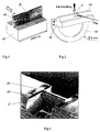
- a sample piece 12 is removed from the solid material, for example from a semiconductor wafer, and a web 11 is worked out on it by mechanical sawing, as is shown, for example, in FIG. 1.
- the sample 12 is about 2600 microns long and the web width is about 20 microns.
- a protective coating is applied to the end face of the web 11 in a partial area where the lamella sample 5 is to be produced, which serves as a mask for the lamella 5 lying underneath and to be etched out. With a focused ion beam (which strikes the web on the end face) FIB), the lamella 5 is now exposed by deep etching.
- a focused ion beam which strikes the web on the end face
- FIG. 2 this is shown schematically by the arrow with the inscription "FIB-etching".
- the sample piece 12 with the lamella sample 5 is now arranged on a sample holder 10 with a diameter of, for example, 3 mm and can now be viewed in the TEM, as is also indicated schematically in FIG. 2 with the arrow and the associated inscription "TEM".
- 3 shows a scanning electron microscopic (SEM) image reproduction of such a sample 5 for better illustration. It can also be seen from this that the FIB etched lamella-like sample (FIB etching) is relatively thick.
- a high waviness of the material can be seen, which also shows that contamination occurs during the etching or sputtering process due to re-covering of the surfaces 6a, b involved.
- the screened FIB ion beam must be operated with energies between 5 keV to 30 keV because of the necessary focusing. This leads to corresponding damage or disruption of the material structure on both sides of the lamella surfaces 6a and 6b of the sample 5, typically to depths of approximately 20 nm.
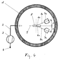
- an FIB sample which already has a corresponding lamella structure 5 is now arranged in a vacuum recipient 1 in its sample arrangement axis or plane 9 in order to be subsequently treated there accordingly.
- the recipient 1 is evacuated in a known manner via a pump line 2 with a vacuum pump 3, for example a turbo-vacuum pump, with a pump outlet 4.
- a vacuum pump 3 for example a turbo-vacuum pump
- an ion source 7 is arranged in the vacuum chamber 1, which can be directed obliquely at an angle ⁇ with respect to the sample arrangement plane 9 with its ion beam 8 onto the sample surfaces 6a and 6b.
- the sample 5 can be etched on both sides of its surfaces 6a and 6b with the ion source 7 by the ion bombardment and can thus be thinned to the desired extent.
- the ion beam 8 is to be directed alternately 8a, b both to one side 6a and to the other side 6b of the sample 5. This mutual etching of the two sides of the sample 6a, b prevents re-loading and thus contamination of the surfaces 6a, b.
- the mutual etching of the surfaces 6a and 6b is advantageously carried out by periodically changing the sides of the sample 5.
- a bombardment angle range +/- ⁇ has to be run through according to the invention, which runs through the values in the range +/- 4 ° to +/- 45 °.
- Particularly good results are achieved for the shot angle range +/- ⁇ in the range +/- 4 ° to +/- 20 °.
- care must be taken that each side of the sample is processed at least twice with the ion beam. However, it is particularly advantageous if each side of the sample is processed several times. The duration of the exposure to radiation per processing step depends on the initial thickness and the amount of material to be thinned.
- the known FIB samples and the desired results are advantageously carried out in a range from a few seconds to a few minutes per side and step. According to the invention, as much as possible should be removed from the disturbed structural area of the FIB sample surface 6a, b.
- the maximum remaining interference depth of the two surfaces 6a, b should have a maximum of 10 nm after processing, whereby according to the inventive procedure preferably a maximum of 5 nm disturbed material should remain on the surfaces 6a, b.
- Such high-resolution samples for HRTEM use are especially for sample materials in the range of semiconductor examinations, in particular for semiconductors, the materials contain suitable as Si, GaAs, Ge.
- the aftertreatment according to the invention can also be particularly good be automated by using corresponding programmable Controls.
- the timing, the number of etching steps and the firing angle, as well as the movement course preset as desired or programmed and processed automatically become.
- the entire preparation process can thus automated with the help of a preparation program and individually to the samples to be created 5 can be adjusted.
- the automatic aftertreatment of Sample 5 does not therefore require the constant presence of the Operator and is therefore time-saving, reproducible and economically feasible.
- FIB-Schhitt or Slat 5 made of silicon material with a platinum protective layer 13 used.
- the lamella is 6 ⁇ m deep including the platinum protective layer 13 and 13 ⁇ m wide.
- the acceleration voltage of the Ion source 7 was 2 keV and the ion current was 1.3 mA.
- the changing firing angle +/- ⁇ of maximum +/- 15 ° the sample was +/- 20 ° with respect to the lamella surface oscillates, i.e. with respect to the direction of the ion beam tilts back and forth in intervals of approximately 0.1 Hz, in the preferred direction to avoid the etching beam on the sample.
- the sample was first etched for a total of eight minutes then looked at and then etched on for ten minutes and also looked at and finally again with three minutes further etched, i.e. etched for a total of 21 minutes.
Landscapes
- Chemical & Material Sciences (AREA)
- Physics & Mathematics (AREA)
- Analytical Chemistry (AREA)
- General Health & Medical Sciences (AREA)
- Life Sciences & Earth Sciences (AREA)
- Biochemistry (AREA)
- Health & Medical Sciences (AREA)
- General Physics & Mathematics (AREA)
- Immunology (AREA)
- Pathology (AREA)
- Engineering & Computer Science (AREA)
- Plasma & Fusion (AREA)
- Sampling And Sample Adjustment (AREA)
Applications Claiming Priority (2)
| Application Number | Priority Date | Filing Date | Title |
|---|---|---|---|
| CH2252003 | 2003-02-15 | ||
| CH2252003 | 2003-02-15 |
Publications (1)
| Publication Number | Publication Date |
|---|---|
| EP1447656A1 true EP1447656A1 (de) | 2004-08-18 |
Family
ID=32661009
Family Applications (1)
| Application Number | Title | Priority Date | Filing Date |
|---|---|---|---|
| EP20030029595 Withdrawn EP1447656A1 (de) | 2003-02-15 | 2003-12-23 | Proben für die Transmissions-Elektronen-Mikroskopie |
Country Status (3)
| Country | Link |
|---|---|
| US (1) | US7002152B2 (ja) |
| EP (1) | EP1447656A1 (ja) |
| JP (1) | JP2004245841A (ja) |
Cited By (3)
| Publication number | Priority date | Publication date | Assignee | Title |
|---|---|---|---|---|
| WO2008106815A3 (de) * | 2007-03-06 | 2008-10-23 | Bal Tec Ag | Verfahren zur herstellung einer probe für die elektronenmikroskopie |
| EP2674742A3 (en) * | 2012-06-11 | 2014-02-12 | Fei Company | Lamella creation method and device using fixed-angle beam and rotating sample stage |
| CN104101510A (zh) * | 2013-04-04 | 2014-10-15 | 弗劳恩霍弗应用技术研究院 | 制造样品的方法和装置以及样品 |
Families Citing this family (28)
| Publication number | Priority date | Publication date | Assignee | Title |
|---|---|---|---|---|
| US8058142B2 (en) | 1996-11-04 | 2011-11-15 | Besang Inc. | Bonded semiconductor structure and method of making the same |
| JP4335497B2 (ja) * | 2002-07-12 | 2009-09-30 | エスアイアイ・ナノテクノロジー株式会社 | イオンビーム装置およびイオンビーム加工方法 |
| US7799675B2 (en) * | 2003-06-24 | 2010-09-21 | Sang-Yun Lee | Bonded semiconductor structure and method of fabricating the same |
| US7632738B2 (en) * | 2003-06-24 | 2009-12-15 | Sang-Yun Lee | Wafer bonding method |
| US8471263B2 (en) | 2003-06-24 | 2013-06-25 | Sang-Yun Lee | Information storage system which includes a bonded semiconductor structure |
| US20100190334A1 (en) * | 2003-06-24 | 2010-07-29 | Sang-Yun Lee | Three-dimensional semiconductor structure and method of manufacturing the same |
| TW200500599A (en) * | 2003-06-24 | 2005-01-01 | Au Optronics Corp | OLED electron microscope test specimen and its manufacturing method |
| US7863748B2 (en) * | 2003-06-24 | 2011-01-04 | Oh Choonsik | Semiconductor circuit and method of fabricating the same |
| US7867822B2 (en) | 2003-06-24 | 2011-01-11 | Sang-Yun Lee | Semiconductor memory device |
| US8071438B2 (en) | 2003-06-24 | 2011-12-06 | Besang Inc. | Semiconductor circuit |
| US20060219919A1 (en) * | 2003-11-11 | 2006-10-05 | Moore Thomas M | TEM sample holder and method of forming same |
| US8723144B2 (en) * | 2004-07-14 | 2014-05-13 | Applied Materials Israel, Ltd. | Apparatus for sample formation and microanalysis in a vacuum chamber |
| JP4486462B2 (ja) * | 2004-09-29 | 2010-06-23 | 日本電子株式会社 | 試料作製方法および試料作製装置 |
| US8455978B2 (en) | 2010-05-27 | 2013-06-04 | Sang-Yun Lee | Semiconductor circuit structure and method of making the same |
| US8367524B2 (en) * | 2005-03-29 | 2013-02-05 | Sang-Yun Lee | Three-dimensional integrated circuit structure |
| JP5959139B2 (ja) * | 2006-10-20 | 2016-08-02 | エフ・イ−・アイ・カンパニー | S/temのサンプルを分析する方法 |
| JP5266236B2 (ja) | 2006-10-20 | 2013-08-21 | エフ・イ−・アイ・カンパニー | サンプル抽出および取り扱いのための方法および装置 |
| EP2151848A1 (en) | 2008-08-07 | 2010-02-10 | FEI Company | Method of machining a work piece with a focused particle beam |
| DE102009008166A1 (de) * | 2009-02-10 | 2010-09-02 | Carl Zeiss Nts Gmbh | Verfahren zur Abscheidung von Schutzstrukturen |
| US8723335B2 (en) | 2010-05-20 | 2014-05-13 | Sang-Yun Lee | Semiconductor circuit structure and method of forming the same using a capping layer |
| DE102010032894B4 (de) | 2010-07-30 | 2013-08-22 | Carl Zeiss Microscopy Gmbh | Tem-Lamelle, Verfahren zu ihrer Herstellung und Vorrichtung zum Ausführen des Verfahrens |
| US8624185B2 (en) * | 2010-09-17 | 2014-01-07 | Carl Zeiss Microscopy, Llc | Sample preparation |
| JP5657435B2 (ja) * | 2011-03-15 | 2015-01-21 | 日本電子株式会社 | 薄膜試料作製方法 |
| US9360401B2 (en) * | 2014-09-24 | 2016-06-07 | Inotera Memories, Inc. | Sample stack structure and method for preparing the same |
| WO2016067039A1 (en) * | 2014-10-29 | 2016-05-06 | Omniprobe, Inc | Rapid tem sample preparation method with backside fib milling |
| CN104913957B (zh) * | 2015-05-04 | 2019-07-19 | 中国石油化工股份有限公司 | Tem原位观察材料基体/钝化膜界面结构的样品制备方法 |
| CN113804521B (zh) * | 2020-06-16 | 2022-12-13 | 中国科学院上海硅酸盐研究所 | 一种用于超薄样品制备的样品台 |
| CN113899764A (zh) * | 2021-09-27 | 2022-01-07 | 中国科学院广州地球化学研究所 | 一种基于离子减薄的电子显微三维重构地质样品制样方法 |
Citations (6)
| Publication number | Priority date | Publication date | Assignee | Title |
|---|---|---|---|---|
| US4128765A (en) * | 1976-10-29 | 1978-12-05 | Joseph Franks | Ion beam machining techniques and apparatus |
| US5009743A (en) * | 1989-11-06 | 1991-04-23 | Gatan Incorporated | Chemically-assisted ion beam milling system for the preparation of transmission electron microscope specimens |
| US5472566A (en) * | 1994-11-14 | 1995-12-05 | Gatan, Inc. | Specimen holder and apparatus for two-sided ion milling system |
| US5986264A (en) * | 1995-04-29 | 1999-11-16 | Bal-Tec A.G. | Ion beam preparation device for electron microscopy |
| US6194720B1 (en) * | 1998-06-24 | 2001-02-27 | Micron Technology, Inc. | Preparation of transmission electron microscope samples |
| US6218663B1 (en) * | 1995-07-25 | 2001-04-17 | Nmi Naturwissenschaftliches Und Medizinisches | Process and device for ion thinning in a high resolution transmission electron microscope |
Family Cites Families (2)
| Publication number | Priority date | Publication date | Assignee | Title |
|---|---|---|---|---|
| US6039000A (en) * | 1998-02-11 | 2000-03-21 | Micrion Corporation | Focused particle beam systems and methods using a tilt column |
| US6768110B2 (en) * | 2000-06-21 | 2004-07-27 | Gatan, Inc. | Ion beam milling system and method for electron microscopy specimen preparation |
-
2003
- 2003-04-10 US US10/410,828 patent/US7002152B2/en not_active Expired - Lifetime
- 2003-12-23 EP EP20030029595 patent/EP1447656A1/de not_active Withdrawn
-
2004
- 2004-02-12 JP JP2004035289A patent/JP2004245841A/ja active Pending
Patent Citations (6)
| Publication number | Priority date | Publication date | Assignee | Title |
|---|---|---|---|---|
| US4128765A (en) * | 1976-10-29 | 1978-12-05 | Joseph Franks | Ion beam machining techniques and apparatus |
| US5009743A (en) * | 1989-11-06 | 1991-04-23 | Gatan Incorporated | Chemically-assisted ion beam milling system for the preparation of transmission electron microscope specimens |
| US5472566A (en) * | 1994-11-14 | 1995-12-05 | Gatan, Inc. | Specimen holder and apparatus for two-sided ion milling system |
| US5986264A (en) * | 1995-04-29 | 1999-11-16 | Bal-Tec A.G. | Ion beam preparation device for electron microscopy |
| US6218663B1 (en) * | 1995-07-25 | 2001-04-17 | Nmi Naturwissenschaftliches Und Medizinisches | Process and device for ion thinning in a high resolution transmission electron microscope |
| US6194720B1 (en) * | 1998-06-24 | 2001-02-27 | Micron Technology, Inc. | Preparation of transmission electron microscope samples |
Non-Patent Citations (3)
| Title |
|---|
| AKIRA YAMAGUCHI ET AL: "TRANSMISSION ELECTRON MICROSCOPY SPECIMEN PREPARATION TECHNIQUE USING FOCUSED ION BEAM FABRICATION: APPLICATION TO GAAS METAL- SEMICONDUCTOR FIELD EFFECT TRANSISTORS", JOURNAL OF VACUUM SCIENCE AND TECHNOLOGY: PART B, AMERICAN INSTITUTE OF PHYSICS. NEW YORK, US, vol. 11, no. 6, 1 November 1993 (1993-11-01), pages 2016 - 2020, XP000423384, ISSN: 0734-211X * |
| ASSAYAG G B ET AL: "LOCALIZED THINNING OF GAAS/GAALAS NANOSTRUCTURES BY A COMBINED SCANNING ELECTRON MICROGRAPH/FOCUS ION BEAM SYSTEM FOR HIGH-QUALITY CROSS-SECTIONAL TRANSMISSION ELECTRON MICROSCOPY SAMPLES", JOURNAL OF VACUUM SCIENCE AND TECHNOLOGY: PART B, AMERICAN INSTITUTE OF PHYSICS. NEW YORK, US, vol. 11, no. 3, 1 May 1993 (1993-05-01), pages 531 - 535, XP000383150, ISSN: 0734-211X * |
| ISHITANI T ET AL: "FOCUSED ION BEAM SYSTEM FOR TEM SAMPLE PREPARATION", HITACHI REVIEW, HITACHI LTD. TOKYO, JP, vol. 45, no. 1, 1 February 1996 (1996-02-01), pages 19 - 24, XP000593685, ISSN: 0018-277X * |
Cited By (5)
| Publication number | Priority date | Publication date | Assignee | Title |
|---|---|---|---|---|
| WO2008106815A3 (de) * | 2007-03-06 | 2008-10-23 | Bal Tec Ag | Verfahren zur herstellung einer probe für die elektronenmikroskopie |
| US8168960B2 (en) | 2007-03-06 | 2012-05-01 | Leica Mikrosysteme Gmbh | Method for the production of a sample for electron microscopy |
| EP2674742A3 (en) * | 2012-06-11 | 2014-02-12 | Fei Company | Lamella creation method and device using fixed-angle beam and rotating sample stage |
| US9733164B2 (en) | 2012-06-11 | 2017-08-15 | Fei Company | Lamella creation method and device using fixed-angle beam and rotating sample stage |
| CN104101510A (zh) * | 2013-04-04 | 2014-10-15 | 弗劳恩霍弗应用技术研究院 | 制造样品的方法和装置以及样品 |
Also Published As
| Publication number | Publication date |
|---|---|
| US7002152B2 (en) | 2006-02-21 |
| JP2004245841A (ja) | 2004-09-02 |
| US20040164242A1 (en) | 2004-08-26 |
Similar Documents
| Publication | Publication Date | Title |
|---|---|---|
| EP1447656A1 (de) | Proben für die Transmissions-Elektronen-Mikroskopie | |
| EP2132550B1 (de) | Verfahren zur herstellung einer probe für die elektronenmikroskopie | |
| EP0120834B1 (de) | Optisch strukturiertes Filter und Verfahren zu dessen Herstellung | |
| EP2667384B1 (de) | Röntgenanalysegerät mit einkristalliner Röntgenblende und Verfahren zur Herstellung einer einkristallinen Röntgenblende | |
| EP2504725B1 (de) | Verfahren und vorrichtung zur herstellung einer fresnel-zonenplatte | |
| DE2823829C2 (de) | Verfahren und Vorrichtung zum Verändern des Strahlquerschnitts eines Strahls elektrisch geladener Teilchen | |
| DE102010024625A1 (de) | Verfahren zum Bearbeiten eines Objekts | |
| EP2175456A2 (de) | Röntgenanalyseinstrument mit verfahrbarem Aperturfenster | |
| DE112013004612B4 (de) | Mit einem Strahl geladener Teilchen arbeitende Vorrichtung und Probenpräparationsverfahren | |
| DE102010032894A1 (de) | Tem-Lamelle, Verfahren zu ihrer Herstellung und Vorrichtung zum Ausführen des Verfahrens | |
| EP3538293A1 (de) | Verfahren zur schichtweisen additiven fertigung von bauteilen und zugehöriges computerprogrammprodukt | |
| DE69133256T2 (de) | Rasterelekronenmikroskop und Bilderzeugungsverfahren | |
| EP3101406A1 (de) | Verfahren zur präparation einer probe für die mikrostrukturdiagnostik sowie probe für die mikrostrukturdiagnostik | |
| EP3153838B1 (de) | Verfahren zur präparation einer probe für die mikrostrukturdiagnostik sowie probe für die mikrostrukturdiagnostik | |
| DE102017203553A1 (de) | Objektpräparationseinrichtung und Teilchenstrahlgerät mit einer Objektpräparationseinrichtung sowie Verfahren zum Betrieb des Teilchenstrahlgeräts | |
| DE112014003194T5 (de) | Verfahren zu Bearbeitung einer Probe in einem mindestens zwei Partikelstrahlen erzeugenden Gerät und Gerät zur Durchführung des Verfahrens | |
| DE102013102537B4 (de) | Proben-vorbereitungsverfahren | |
| DE19647975C2 (de) | Reflexionselektronenmikroskop | |
| EP1309896A2 (de) | Lochmaske und verfahren zur herstellung einer lochmaske | |
| DE102015204478B4 (de) | Verfahren zum Glätten einer Oberfläche und optisches Element | |
| DE102004001173B4 (de) | Verfahren zur Herstellung von zur Untersuchung mittels Transmissionselektronenmikroskopie geeigneten Proben | |
| DE112006001006T5 (de) | Bearbeitungsverfahren mit einem fokussierten Ionenstrahl und Einrichtung zur Durchführung des Verfahrens | |
| DE10358036B4 (de) | Verfahren zum Charakterisieren einer Tiefenstruktur in einem Substrat | |
| DE102005053324B4 (de) | Target für eine Mikrofocus- oder Nanofocus-Röntgenröhre | |
| DE19545721A1 (de) | Verfahren zur Herstellung und Justierung von Mikrolinsen auf Faser- und Laser-Enden |
Legal Events
| Date | Code | Title | Description |
|---|---|---|---|
| PUAI | Public reference made under article 153(3) epc to a published international application that has entered the european phase |
Free format text: ORIGINAL CODE: 0009012 |
|
| AK | Designated contracting states |
Kind code of ref document: A1 Designated state(s): AT BE BG CH CY CZ DE DK EE ES FI FR GB GR HU IE IT LI LU MC NL PT RO SE SI SK TR |
|
| AX | Request for extension of the european patent |
Extension state: AL LT LV MK |
|
| 17P | Request for examination filed |
Effective date: 20050218 |
|
| AKX | Designation fees paid |
Designated state(s): AT BE BG CH CY CZ DE DK EE ES FI FR GB GR HU IE IT LI LU MC NL PT RO SE SI SK TR |
|
| 17Q | First examination report despatched |
Effective date: 20080306 |
|
| RAP1 | Party data changed (applicant data changed or rights of an application transferred) |
Owner name: LEICA MIKROSYSTEME GMBH |
|
| 19U | Interruption of proceedings before grant |
Effective date: 20130424 |
|
| 19W | Proceedings resumed before grant after interruption of proceedings |
Effective date: 20150201 |
|
| STAA | Information on the status of an ep patent application or granted ep patent |
Free format text: STATUS: THE APPLICATION IS DEEMED TO BE WITHDRAWN |
|
| 18D | Application deemed to be withdrawn |
Effective date: 20150918 |