EP1445861A2 - Electronic device and method of manufacturing the same - Google Patents
Electronic device and method of manufacturing the same Download PDFInfo
- Publication number
- EP1445861A2 EP1445861A2 EP04000078A EP04000078A EP1445861A2 EP 1445861 A2 EP1445861 A2 EP 1445861A2 EP 04000078 A EP04000078 A EP 04000078A EP 04000078 A EP04000078 A EP 04000078A EP 1445861 A2 EP1445861 A2 EP 1445861A2
- Authority
- EP
- European Patent Office
- Prior art keywords
- gold
- substrate
- chip
- bonding
- electrodes
- Prior art date
- Legal status (The legal status is an assumption and is not a legal conclusion. Google has not performed a legal analysis and makes no representation as to the accuracy of the status listed.)
- Ceased
Links
Images





Classifications
-
- H—ELECTRICITY
- H03—ELECTRONIC CIRCUITRY
- H03H—IMPEDANCE NETWORKS, e.g. RESONANT CIRCUITS; RESONATORS
- H03H9/00—Networks comprising electromechanical or electro-acoustic elements; Electromechanical resonators
- H03H9/02—Details
- H03H9/05—Holders or supports
- H03H9/058—Holders or supports for surface acoustic wave devices
- H03H9/059—Holders or supports for surface acoustic wave devices consisting of mounting pads or bumps
-
- B—PERFORMING OPERATIONS; TRANSPORTING
- B81—MICROSTRUCTURAL TECHNOLOGY
- B81B—MICROSTRUCTURAL DEVICES OR SYSTEMS, e.g. MICROMECHANICAL DEVICES
- B81B7/00—Microstructural systems ; Auxiliary parts of microstructural devices or systems
- B81B7/0032—Packages or encapsulation
- B81B7/007—Interconnections between the MEMS and external electrical signals
-
- B—PERFORMING OPERATIONS; TRANSPORTING
- B81—MICROSTRUCTURAL TECHNOLOGY
- B81C—PROCESSES OR APPARATUS SPECIALLY ADAPTED FOR THE MANUFACTURE OR TREATMENT OF MICROSTRUCTURAL DEVICES OR SYSTEMS
- B81C1/00—Manufacture or treatment of devices or systems in or on a substrate
- B81C1/00015—Manufacture or treatment of devices or systems in or on a substrate for manufacturing microsystems
- B81C1/00261—Processes for packaging MEMS devices
- B81C1/00269—Bonding of solid lids or wafers to the substrate
-
- H—ELECTRICITY
- H03—ELECTRONIC CIRCUITRY
- H03H—IMPEDANCE NETWORKS, e.g. RESONANT CIRCUITS; RESONATORS
- H03H3/00—Apparatus or processes specially adapted for the manufacture of impedance networks, resonating circuits, resonators
- H03H3/007—Apparatus or processes specially adapted for the manufacture of impedance networks, resonating circuits, resonators for the manufacture of electromechanical resonators or networks
-
- H—ELECTRICITY
- H03—ELECTRONIC CIRCUITRY
- H03H—IMPEDANCE NETWORKS, e.g. RESONANT CIRCUITS; RESONATORS
- H03H9/00—Networks comprising electromechanical or electro-acoustic elements; Electromechanical resonators
- H03H9/02—Details
- H03H9/05—Holders or supports
- H03H9/10—Mounting in enclosures
- H03H9/1064—Mounting in enclosures for surface acoustic wave [SAW] devices
- H03H9/1078—Mounting in enclosures for surface acoustic wave [SAW] devices the enclosure being defined by a foil covering the non-active sides of the SAW device
-
- H—ELECTRICITY
- H10—SEMICONDUCTOR DEVICES; ELECTRIC SOLID-STATE DEVICES NOT OTHERWISE PROVIDED FOR
- H10W—GENERIC PACKAGES, INTERCONNECTIONS, CONNECTORS OR OTHER CONSTRUCTIONAL DETAILS OF DEVICES COVERED BY CLASS H10
- H10W42/00—Arrangements for protection of devices
- H10W42/20—Arrangements for protection of devices protecting against electromagnetic or particle radiation, e.g. light, X-rays, gamma-rays or electrons
-
- H—ELECTRICITY
- H10—SEMICONDUCTOR DEVICES; ELECTRIC SOLID-STATE DEVICES NOT OTHERWISE PROVIDED FOR
- H10W—GENERIC PACKAGES, INTERCONNECTIONS, CONNECTORS OR OTHER CONSTRUCTIONAL DETAILS OF DEVICES COVERED BY CLASS H10
- H10W76/00—Containers; Fillings or auxiliary members therefor; Seals
- H10W76/60—Seals
-
- B—PERFORMING OPERATIONS; TRANSPORTING
- B81—MICROSTRUCTURAL TECHNOLOGY
- B81C—PROCESSES OR APPARATUS SPECIALLY ADAPTED FOR THE MANUFACTURE OR TREATMENT OF MICROSTRUCTURAL DEVICES OR SYSTEMS
- B81C2203/00—Forming microstructural systems
- B81C2203/01—Packaging MEMS
- B81C2203/0172—Seals
- B81C2203/019—Seals characterised by the material or arrangement of seals between parts
-
- B—PERFORMING OPERATIONS; TRANSPORTING
- B81—MICROSTRUCTURAL TECHNOLOGY
- B81C—PROCESSES OR APPARATUS SPECIALLY ADAPTED FOR THE MANUFACTURE OR TREATMENT OF MICROSTRUCTURAL DEVICES OR SYSTEMS
- B81C2203/00—Forming microstructural systems
- B81C2203/03—Bonding two components
- B81C2203/033—Thermal bonding
- B81C2203/036—Fusion bonding
-
- H—ELECTRICITY
- H03—ELECTRONIC CIRCUITRY
- H03H—IMPEDANCE NETWORKS, e.g. RESONANT CIRCUITS; RESONATORS
- H03H3/00—Apparatus or processes specially adapted for the manufacture of impedance networks, resonating circuits, resonators
- H03H3/007—Apparatus or processes specially adapted for the manufacture of impedance networks, resonating circuits, resonators for the manufacture of electromechanical resonators or networks
- H03H3/08—Apparatus or processes specially adapted for the manufacture of impedance networks, resonating circuits, resonators for the manufacture of electromechanical resonators or networks for the manufacture of resonators or networks using surface acoustic waves
-
- H—ELECTRICITY
- H10—SEMICONDUCTOR DEVICES; ELECTRIC SOLID-STATE DEVICES NOT OTHERWISE PROVIDED FOR
- H10W—GENERIC PACKAGES, INTERCONNECTIONS, CONNECTORS OR OTHER CONSTRUCTIONAL DETAILS OF DEVICES COVERED BY CLASS H10
- H10W72/00—Interconnections or connectors in packages
- H10W72/01—Manufacture or treatment
- H10W72/012—Manufacture or treatment of bump connectors, dummy bumps or thermal bumps
- H10W72/01231—Manufacture or treatment of bump connectors, dummy bumps or thermal bumps using blanket deposition
- H10W72/01233—Manufacture or treatment of bump connectors, dummy bumps or thermal bumps using blanket deposition in liquid form, e.g. spin coating, spray coating or immersion coating
- H10W72/01235—Manufacture or treatment of bump connectors, dummy bumps or thermal bumps using blanket deposition in liquid form, e.g. spin coating, spray coating or immersion coating by plating, e.g. electroless plating or electroplating
-
- H—ELECTRICITY
- H10—SEMICONDUCTOR DEVICES; ELECTRIC SOLID-STATE DEVICES NOT OTHERWISE PROVIDED FOR
- H10W—GENERIC PACKAGES, INTERCONNECTIONS, CONNECTORS OR OTHER CONSTRUCTIONAL DETAILS OF DEVICES COVERED BY CLASS H10
- H10W72/00—Interconnections or connectors in packages
- H10W72/01—Manufacture or treatment
- H10W72/019—Manufacture or treatment of bond pads
- H10W72/01931—Manufacture or treatment of bond pads using blanket deposition
- H10W72/01938—Manufacture or treatment of bond pads using blanket deposition in gaseous form, e.g. by CVD or PVD
-
- H—ELECTRICITY
- H10—SEMICONDUCTOR DEVICES; ELECTRIC SOLID-STATE DEVICES NOT OTHERWISE PROVIDED FOR
- H10W—GENERIC PACKAGES, INTERCONNECTIONS, CONNECTORS OR OTHER CONSTRUCTIONAL DETAILS OF DEVICES COVERED BY CLASS H10
- H10W72/00—Interconnections or connectors in packages
- H10W72/01—Manufacture or treatment
- H10W72/0198—Manufacture or treatment batch processes
-
- H—ELECTRICITY
- H10—SEMICONDUCTOR DEVICES; ELECTRIC SOLID-STATE DEVICES NOT OTHERWISE PROVIDED FOR
- H10W—GENERIC PACKAGES, INTERCONNECTIONS, CONNECTORS OR OTHER CONSTRUCTIONAL DETAILS OF DEVICES COVERED BY CLASS H10
- H10W72/00—Interconnections or connectors in packages
- H10W72/071—Connecting or disconnecting
- H10W72/072—Connecting or disconnecting of bump connectors
-
- H—ELECTRICITY
- H10—SEMICONDUCTOR DEVICES; ELECTRIC SOLID-STATE DEVICES NOT OTHERWISE PROVIDED FOR
- H10W—GENERIC PACKAGES, INTERCONNECTIONS, CONNECTORS OR OTHER CONSTRUCTIONAL DETAILS OF DEVICES COVERED BY CLASS H10
- H10W72/00—Interconnections or connectors in packages
- H10W72/071—Connecting or disconnecting
- H10W72/072—Connecting or disconnecting of bump connectors
- H10W72/07221—Aligning
- H10W72/07227—Aligning involving guiding structures, e.g. spacers or supporting members
-
- H—ELECTRICITY
- H10—SEMICONDUCTOR DEVICES; ELECTRIC SOLID-STATE DEVICES NOT OTHERWISE PROVIDED FOR
- H10W—GENERIC PACKAGES, INTERCONNECTIONS, CONNECTORS OR OTHER CONSTRUCTIONAL DETAILS OF DEVICES COVERED BY CLASS H10
- H10W72/00—Interconnections or connectors in packages
- H10W72/071—Connecting or disconnecting
- H10W72/072—Connecting or disconnecting of bump connectors
- H10W72/07231—Techniques
- H10W72/07232—Compression bonding, e.g. thermocompression bonding
-
- H—ELECTRICITY
- H10—SEMICONDUCTOR DEVICES; ELECTRIC SOLID-STATE DEVICES NOT OTHERWISE PROVIDED FOR
- H10W—GENERIC PACKAGES, INTERCONNECTIONS, CONNECTORS OR OTHER CONSTRUCTIONAL DETAILS OF DEVICES COVERED BY CLASS H10
- H10W72/00—Interconnections or connectors in packages
- H10W72/071—Connecting or disconnecting
- H10W72/072—Connecting or disconnecting of bump connectors
- H10W72/07231—Techniques
- H10W72/07236—Soldering or alloying
-
- H—ELECTRICITY
- H10—SEMICONDUCTOR DEVICES; ELECTRIC SOLID-STATE DEVICES NOT OTHERWISE PROVIDED FOR
- H10W—GENERIC PACKAGES, INTERCONNECTIONS, CONNECTORS OR OTHER CONSTRUCTIONAL DETAILS OF DEVICES COVERED BY CLASS H10
- H10W72/00—Interconnections or connectors in packages
- H10W72/071—Connecting or disconnecting
- H10W72/073—Connecting or disconnecting of die-attach connectors
-
- H—ELECTRICITY
- H10—SEMICONDUCTOR DEVICES; ELECTRIC SOLID-STATE DEVICES NOT OTHERWISE PROVIDED FOR
- H10W—GENERIC PACKAGES, INTERCONNECTIONS, CONNECTORS OR OTHER CONSTRUCTIONAL DETAILS OF DEVICES COVERED BY CLASS H10
- H10W72/00—Interconnections or connectors in packages
- H10W72/071—Connecting or disconnecting
- H10W72/073—Connecting or disconnecting of die-attach connectors
- H10W72/07331—Connecting techniques
- H10W72/07332—Compression bonding, e.g. thermocompression bonding
-
- H—ELECTRICITY
- H10—SEMICONDUCTOR DEVICES; ELECTRIC SOLID-STATE DEVICES NOT OTHERWISE PROVIDED FOR
- H10W—GENERIC PACKAGES, INTERCONNECTIONS, CONNECTORS OR OTHER CONSTRUCTIONAL DETAILS OF DEVICES COVERED BY CLASS H10
- H10W72/00—Interconnections or connectors in packages
- H10W72/071—Connecting or disconnecting
- H10W72/074—Connecting or disconnecting of anisotropic conductive adhesives
-
- H—ELECTRICITY
- H10—SEMICONDUCTOR DEVICES; ELECTRIC SOLID-STATE DEVICES NOT OTHERWISE PROVIDED FOR
- H10W—GENERIC PACKAGES, INTERCONNECTIONS, CONNECTORS OR OTHER CONSTRUCTIONAL DETAILS OF DEVICES COVERED BY CLASS H10
- H10W72/00—Interconnections or connectors in packages
- H10W72/20—Bump connectors, e.g. solder bumps or copper pillars; Dummy bumps; Thermal bumps
- H10W72/251—Materials
-
- H—ELECTRICITY
- H10—SEMICONDUCTOR DEVICES; ELECTRIC SOLID-STATE DEVICES NOT OTHERWISE PROVIDED FOR
- H10W—GENERIC PACKAGES, INTERCONNECTIONS, CONNECTORS OR OTHER CONSTRUCTIONAL DETAILS OF DEVICES COVERED BY CLASS H10
- H10W72/00—Interconnections or connectors in packages
- H10W72/20—Bump connectors, e.g. solder bumps or copper pillars; Dummy bumps; Thermal bumps
- H10W72/251—Materials
- H10W72/252—Materials comprising solid metals or solid metalloids, e.g. PbSn, Ag or Cu
-
- H—ELECTRICITY
- H10—SEMICONDUCTOR DEVICES; ELECTRIC SOLID-STATE DEVICES NOT OTHERWISE PROVIDED FOR
- H10W—GENERIC PACKAGES, INTERCONNECTIONS, CONNECTORS OR OTHER CONSTRUCTIONAL DETAILS OF DEVICES COVERED BY CLASS H10
- H10W72/00—Interconnections or connectors in packages
- H10W72/20—Bump connectors, e.g. solder bumps or copper pillars; Dummy bumps; Thermal bumps
- H10W72/29—Bond pads specially adapted therefor
-
- H—ELECTRICITY
- H10—SEMICONDUCTOR DEVICES; ELECTRIC SOLID-STATE DEVICES NOT OTHERWISE PROVIDED FOR
- H10W—GENERIC PACKAGES, INTERCONNECTIONS, CONNECTORS OR OTHER CONSTRUCTIONAL DETAILS OF DEVICES COVERED BY CLASS H10
- H10W72/00—Interconnections or connectors in packages
- H10W72/30—Die-attach connectors
- H10W72/321—Structures or relative sizes of die-attach connectors
- H10W72/325—Die-attach connectors having a filler embedded in a matrix
-
- H—ELECTRICITY
- H10—SEMICONDUCTOR DEVICES; ELECTRIC SOLID-STATE DEVICES NOT OTHERWISE PROVIDED FOR
- H10W—GENERIC PACKAGES, INTERCONNECTIONS, CONNECTORS OR OTHER CONSTRUCTIONAL DETAILS OF DEVICES COVERED BY CLASS H10
- H10W72/00—Interconnections or connectors in packages
- H10W72/30—Die-attach connectors
- H10W72/351—Materials of die-attach connectors
-
- H—ELECTRICITY
- H10—SEMICONDUCTOR DEVICES; ELECTRIC SOLID-STATE DEVICES NOT OTHERWISE PROVIDED FOR
- H10W—GENERIC PACKAGES, INTERCONNECTIONS, CONNECTORS OR OTHER CONSTRUCTIONAL DETAILS OF DEVICES COVERED BY CLASS H10
- H10W72/00—Interconnections or connectors in packages
- H10W72/30—Die-attach connectors
- H10W72/351—Materials of die-attach connectors
- H10W72/352—Materials of die-attach connectors comprising metals or metalloids, e.g. solders
-
- H—ELECTRICITY
- H10—SEMICONDUCTOR DEVICES; ELECTRIC SOLID-STATE DEVICES NOT OTHERWISE PROVIDED FOR
- H10W—GENERIC PACKAGES, INTERCONNECTIONS, CONNECTORS OR OTHER CONSTRUCTIONAL DETAILS OF DEVICES COVERED BY CLASS H10
- H10W72/00—Interconnections or connectors in packages
- H10W72/30—Die-attach connectors
- H10W72/351—Materials of die-attach connectors
- H10W72/353—Materials of die-attach connectors not comprising solid metals or solid metalloids, e.g. ceramics
-
- H—ELECTRICITY
- H10—SEMICONDUCTOR DEVICES; ELECTRIC SOLID-STATE DEVICES NOT OTHERWISE PROVIDED FOR
- H10W—GENERIC PACKAGES, INTERCONNECTIONS, CONNECTORS OR OTHER CONSTRUCTIONAL DETAILS OF DEVICES COVERED BY CLASS H10
- H10W72/00—Interconnections or connectors in packages
- H10W72/50—Bond wires
- H10W72/551—Materials of bond wires
- H10W72/552—Materials of bond wires comprising metals or metalloids, e.g. silver
- H10W72/5522—Materials of bond wires comprising metals or metalloids, e.g. silver comprising gold [Au]
-
- H—ELECTRICITY
- H10—SEMICONDUCTOR DEVICES; ELECTRIC SOLID-STATE DEVICES NOT OTHERWISE PROVIDED FOR
- H10W—GENERIC PACKAGES, INTERCONNECTIONS, CONNECTORS OR OTHER CONSTRUCTIONAL DETAILS OF DEVICES COVERED BY CLASS H10
- H10W72/00—Interconnections or connectors in packages
- H10W72/90—Bond pads, in general
- H10W72/951—Materials of bond pads
- H10W72/952—Materials of bond pads comprising metals or metalloids, e.g. PbSn, Ag or Cu
-
- H—ELECTRICITY
- H10—SEMICONDUCTOR DEVICES; ELECTRIC SOLID-STATE DEVICES NOT OTHERWISE PROVIDED FOR
- H10W—GENERIC PACKAGES, INTERCONNECTIONS, CONNECTORS OR OTHER CONSTRUCTIONAL DETAILS OF DEVICES COVERED BY CLASS H10
- H10W74/00—Encapsulations, e.g. protective coatings
- H10W74/10—Encapsulations, e.g. protective coatings characterised by their shape or disposition
- H10W74/15—Encapsulations, e.g. protective coatings characterised by their shape or disposition on active surfaces of flip-chip devices, e.g. underfills
-
- H—ELECTRICITY
- H10—SEMICONDUCTOR DEVICES; ELECTRIC SOLID-STATE DEVICES NOT OTHERWISE PROVIDED FOR
- H10W—GENERIC PACKAGES, INTERCONNECTIONS, CONNECTORS OR OTHER CONSTRUCTIONAL DETAILS OF DEVICES COVERED BY CLASS H10
- H10W90/00—Package configurations
- H10W90/701—Package configurations characterised by the relative positions of pads or connectors relative to package parts
- H10W90/721—Package configurations characterised by the relative positions of pads or connectors relative to package parts of bump connectors
- H10W90/724—Package configurations characterised by the relative positions of pads or connectors relative to package parts of bump connectors between a chip and a stacked insulating package substrate, interposer or RDL
-
- H—ELECTRICITY
- H10—SEMICONDUCTOR DEVICES; ELECTRIC SOLID-STATE DEVICES NOT OTHERWISE PROVIDED FOR
- H10W—GENERIC PACKAGES, INTERCONNECTIONS, CONNECTORS OR OTHER CONSTRUCTIONAL DETAILS OF DEVICES COVERED BY CLASS H10
- H10W99/00—Subject matter not provided for in other groups of this subclass
Definitions
- the present invention relates to an electronic component which needs to be sealed in an airtight manner and a method of manufacturing the electronic component part. More particularly, the present invention relates to a technique effective in an application to a surface acoustic wave device.
- a surface acoustic wave device used as a high-frequency filter for portable telephones, etc. is formed in such a manner that a pair of interdigital electrodes are formed on a surface of a piezoelectric monocrystal chip such as a lithium tantalate (LiTaO 3 ) chip or a lithium niobate (LiNbO 3 ) chip (hereinafter referred to as "SAW chip"), the chip is mounted on a package substrate, and input and output electrodes on the package substrate are electrically connected to the pair of interdigital electrodes.
- a piezoelectric monocrystal chip such as a lithium tantalate (LiTaO 3 ) chip or a lithium niobate (LiNbO 3 ) chip
- a SAW chip is die-bonded to a ceramic package substrate while being positioned so that the chip surface on which a surface acoustic wave propagates, i.e., the surface on which the pair of interdigital electrodes are formed, faces upward, and chip electrodes connected to the pair of interdigital electrodes are electrically connected to internal electrodes on the package substrate by bonding using metallic wires mainly formed of Al or Au.
- the chip is thereafter sealed with a metallic cap in an airtight manner to form a surface acoustic wave device.
- the size of surface acoustic wave devices is reduced by eliminating the wire bonding area in such a manner that the SAW chip is flip-chip-connected to the package substrate.
- JP-A-8-316778 discloses a typical device structure relating to such a size reduction method.
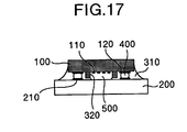
- Fig. 17 shows a diagram schematically showing the device structure.
- a SAW chip 100 having a flow prevention frame 320 formed so as to surround interdigital electrodes 110 is flip-chip-connected to the a package substrate 200 with bumps 400 interposed therebetween, and a sealing resin 310 is injected from a side surface of the SAW chip 100 and is set, thereby forming a surface acoustic wave device.
- the sealing resin 310 is stopped by the flow prevention frame 320 at the time of injection.
- a space 500 is therefore formed on the interdigital electrode 110 surface side to ensure propagation of a surface acoustic wave.
- the bumps 400 are formed by an Au wire bump method and are connected to the package substrate 200 by a solder or an electroconductive resin.
- JP-A-2001-94390 discloses a method in which a substrate and a chip equal in size to each other are used and an electroconductive adhesive is used for peripheral sealing, and which makes it possible to form an electronic component of size equal to the size of the chip.
- This method has a problem that the electrical resistance of the electroconductive adhesive is high and the electroconductive adhesive is not suitable for an airtight package.
- a solution to the problem (1) in terms of manufacture is the development of a sealing method which ensures that the sealing material does not reach the interdigital electrodes.
- a solution to the problem (2) in terms of reliability is the selection of a material capable of complete airtight sealing.
- a solution to the problem (3) in terms of structure is the development of a package device of a SAW chip size considered to be a minimum size.
- a SAW filter is a functional device for extracting a particular frequency in a certain range and such frequency characteristic degradation in a SAW filter is a serious problem. If a SAW filter having such degradation is used in a portable telephone, a fault occurs in the receiving function.
- MCM multi-chip module
- An object of the present invention is to provide a surface acoustic wave device in which a sealing material is prevented from reaching interdigital electrodes, which has improved reliability and producibility, and which can be manufactured at a lower cost, and a method of manufacturing such improved surface acoustic wave device.
- Another object of the present invention is to provide technique capable of limiting degradation in frequency characteristics of a SAW filter.
- Still another object of the present invention is to provide a technique enabling setting of a high temperature level in manufacture of an electronic module using an MCM structure having a SAW filter mounted on an interposer while limiting degradation in frequency characteristics of the electronic module.
- An electronic device provided to achieve the above-described object of the present invention is an electronic component having an electronic circuit element having an electrode and a substrate having a portion which can be connected to the electrode of the electronic circuit element, wherein an electrical connection is made between the electronic circuit element and the substrate, and a device surface on the electronic circuit element is sealed to ensure the formation of a space between the substrate and the electronic circuit element.
- the electrical connection and sealing between a SAW chip and a package substrate in the chip-size electronic device of the present invention are achieved, for example, by two means described below.
- the first means includes making metallic connection by hot pressure bonding for the electrical connection and sealing between the SAW chip and the package substrate.
- Internal electrodes and a sealing portion of a multiple-piece-forming package substrate are plated with Sn, Ag or Au in advance.
- chip electrode portions and chip peripheral portions on a surface acoustic wave wafer are plated with Au.
- the substrate and the surface acoustic wave wafer are positioned in a state of being opposed to each other and are heated and pressed to complete the electrical connections and sealing of a plurality of chips at a time.
- an Au-Sn bond, an Au-Ag bond, an Au-Al bond or an Au-Au bond is formed in the electrode connection and the sealing portion.
- the bonding metals do not flow at the time of connection and the spacing between the SAW chip and the package substrate after connection is substantially equal to the plating thickness between the SAW chip and the package substrate, thus ensuring the formation of a space along the SAW chip interdigital electrode portion.
- the second means uses an electroconductive glass having low flowability as a material for the above-described electrical connection and sealing.
- the electroconductive glass frit is printed or fused at the positions of a peripheral portion and electrodes of a SAW chip to be mounted. SAW elements on a wafer are opposed to and placed on the substrate, followed by heating and pressing. The electroconductive glass is thereby fused to the wafer. Thus, a plurality of chips formed on the wafer are sealed at a time and are simultaneously connected electrically.
- a spacer in the form of fine particles formed of spacer glass balls of several microns, spacer glass rods or electroconductive particles may be mixed in the electroconductive glass to secure the desired connection height and to ensure that the desired space can be formed along the SAW chip interdigital electrode portion.
- the chips are separated by cutting with a dicer along the center lines of the sealing portions, thereby obtaining the chip-size surface acoustic wave device.
- grooving at the centers of the sealing portions is performed by sandblasting in the direction of mounting of the SAW chip to a depth reaching the substrate, metalization by evaporation or plating is performed from the upper surface, and the grooved portions are broken or cut by dicing to separate the chips, thus forming the chip-size surface acoustic wave device.
- a chip-size surface acoustic wave device electromagnetically shielded by metalization on the back surface of the device can be obtained.
- the electromagnetic shielding portion and a ground terminal on the substrate may be connected to improve the electromagnetic shielding effect.
- the SAW chip electrodes and the package substrate electrodes be plated with Au in advance in order to reliably establish electrical connections therebetween.
- a metal bonding method using no flux is used as a SAW filter connection method in order to achieve the above-described objects.
- a gold-tin bonding method among metal connection method using no flux may be used in order to broaden the range of selection of bonding materials used for mounting of other electronic components (to enable use of a bonding material having a high melting point) after mounting of the SAW filter.
- Different temperature levels can easily be set because the gold-tin bonding by heating and pressing produces a gold-tin alloy having a melting point of about 280 degrees much higher than the melting point of tin.
- a solder having a melting point higher than the temperature at which the SAW filter is boded and lower than the melting point of the gold-tin alloy can be used after bonding of the SAW filter. If this characteristic is applied to a MCM structure in which a SAW filter having a solder is mounted on an interposer substrate together with other electronic components, the bonding temperature for mounting of the interposer substrate on a mother substrate can be increased.
- bonding of the signal terminal and sealing can be performed in one step if a metal bonding method using no flux is used for this bonding, thereby reducing the number of process steps.
- the same bonding method is used for the signal bump and the sealing bump. More specifically, gold-tin bonding is used for the two kinds of bumps.
- tin is used for metalization on the parts- or module-substrate-side surface
- gold is used for the bump on the SAW-chip side (the electrical connection portion and the sealing portion)
- bonding is performed by heating and pressing the SAW chip.
- connection and sealing are performed at the tin melting point (231.9 degrees)
- a tin-gold compound is formed and the remelting temperature can therefore be increased (to 280 degrees), thus enabling a bonding material having a high melting point to be used for mounting of an interposer on a mother board.
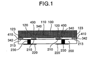
- Fig. 1 is a cross-sectional view of a first embodiment of an electronic device in accordance with the present invention.
- Fig. 2 shows in more detail the first embodiment of the electronic device in accordance with the present invention.
- Figs. 2(a) through 2(d) are diagrams showing the process of assembling the device shown in Fig. 1.
- Fig. 2(a) shows a SAW chip 100 on which wiring is formed and a package substrate 200;
- Fig. 2(b) shows a state where gold bumps 400 and a gold projection 410 for peripheral sealing are formed on the SAW chip 100 and a tin plating 341 is formed on the package substrate 200;
- Fig. 2(c) shows the step of connecting the SAW chip 100 and the package substrate 200 to each other; and
- Fig. 2(d) shows an external appearance after the completion of the process.
- the SAW chip 100 is formed on which interdigital electrodes 110, chip electrodes 120 and a chip electrode 123 for peripheral sealing formed of a metal such as aluminum are formed for wiring, and the package substrate 200 is also formed on which internal electrodes 210 and an internal electrode 213 for peripheral sealing formed of a metal such as copper are formed for wiring.
- a substrate made of a material having high moisture resistance, e.g., a ceramic substrate, a silicon substrate or a glass substrate is preferred as the package substrate 200.
- the gold bumps 400 and the gold projection 410 for peripheral sealing are formed, for example, by plating on the chip electrode 120 and the chip electrode 123 for peripheral sealing, and the surfaces of the internal electrodes 210 and the internal electrode 213 for peripheral sealing are plated with tin.
- the gold bumps 400 may have any shape, e.g., the shape of a rectangular block or a cylindrical shape.
- Tin on the internal electrodes 210 and the internal electrode 213 for peripheral sealing may be formed by a printing method. Positioning between the SAW chip 100 and the package substrate 200 formed as described above is performed (Fig. 2(c)) and heating and pressing are performed on the SAW chip 100 and the package substrate 200.
- the heating temperature is set to a point equal to or higher than the tin melting point (232°C) to melt only tin at the contact interface.
- Tin is molten to react with gold at the interface between the gold bumps 400, the peripheral sealing gold projection 410 and the tin plating 341, thereby forming gold-tin intermetallic compound.
- metallic bonding is effected between the gold bumps 400 and the internal electrodes 210 having the tin plating 341 applied thereto and between the peripheral sealing gold projection 410 and the internal electrode 213 for peripheral sealing having the tin plating 341 applied thereto.
- the melting point of the gold-tin intermetallic compound thereby formed is (metallic connection portions 340 and a connection portion 342 for peripheral sealing) is higher than the tin melting point 232°C. Therefore, even when secondary reflowing for mounting other components is performed, remelting is not caused if the reflowing temperature is lower than the gold-tin intermetallic compound melting point, and the connection between the gold bumps 400 and the internal electrodes 210 having the tin plating 341 applied thereto and the connection between the peripheral sealing gold projection 410 and the internal electrode 213 for peripheral sealing having the tin plate 341 applied thereto are maintained.
- the interdigital electrodes 110 are surrounded by the peripheral sealing gold projection 410 and the gold-tin intermetallic compound on the periphery and are thereby encapsulated in an airtight manner, as shown in Fig. 2(d).
- the peripheral sealing portion may be used as ground.
- the bonding temperature at which bonding is performed at the time of mounting of the interposer substrate on a mother board can be increased.
- Figs. 3(a) through 3(e) are diagrams showing process steps according to a wafer batch forming method for the first embodiment shown in Fig. 1.
- Figs. 3(a) through 3(e) portions corresponding to those in Figs. 1 and 2 are indicated by the same reference numerals.
- Fig. 3(a) shows a package substrate 200 on which wiring is formed before the package substrate 200 is cut into pieces
- Fig. 3(b) shows the package substrate 200 when tin plating 341 is formed before the package substrate 200 is cut into pieces
- Fig. 3(c) shows the step of positioning the package substrate 200 and a SAW wafer 101 having gold bumps 400 and peripheral sealing gold projections 410 formed on electrodes
- Fig. 3(d) shows the step of bonding the SAW wafer 101 and the package substrate 200 by heating and pressing
- Fig. 3(e) shows the step of cutting the combination of the SAW wafer 101 and the package substrate 200 into pieces by dicing after connection.
- the package substrate 200 is formed on which internal electrodes 210 and internal electrodes 213 for peripheral sealing are formed of a metal such as copper before the package substrate 200 is cut into pieces.
- a substrate made of a material having high moisture resistance, e.g., a ceramic substrate, a silicon substrate or a glass substrate is preferred as the package substrate 200.
- the surfaces of the internal electrodes 210 and the internal electrodes 213 for peripheral sealing are plated with tin.
- Tin on the internal electrodes 210 and the internal electrode 213 for peripheral sealing may be formed by using a printing method instead of plating.
- interdigital electrodes 110, chip electrodes 120 and chip electrodes 123 for peripheral sealing formed of a metal such as aluminum are formed for wiring and gold bumps 400 and peripheral sealing gold projections 410 are thereafter formed by plating on the chip electrodes 120 and the chip electrodes 123 for peripheral sealing.
- the gold bumps 400 may have any shape, e.g., the shape of a rectangular block or a cylindrical shape.
- the gold bumps 400 may be formed by performing pole bonding or the like instead of plating. Positioning between the SAW chips 100 and the package substrate 200 is performed (Fig. 3(c)) and heating and pressing are performed on the SAW chips 100 and the package substrate 200.
- the difference between the linear expansion coefficients of the SAW chips on the wafer and the package substrate 200 before connection of pieces can be reduced to limit pattern misalignment between the SAW chips 100 and the package substrate 200 due to thermal shrinkage.
- the heating temperature is set to a point equal to or higher than the tin melting point (232°C) to melt only tin at the contact interface. Tin is molten to react with gold at the interface between the gold bumps 400, the peripheral sealing gold projection 410 and the tin plating 341, thereby forming gold-tin intermetallic compound.
- the interdigital electrodes 110 are surrounded by the peripheral sealing gold projection 410 and the gold-tin intermetallic compound on the periphery and are thereby encapsulated in an airtight manner, as shown in Fig. 3(d).
- the peripheral sealing portion may be used as ground. If the structure shown in Fig. 3(d) is formed by the above-described process, a package having good moisture resistance and improved reliability can be provided.
- the combination of the SAW wafer and the package substrate 200 is cut into pieces by using a dicer, as shown in Fig. 3(e).
- the first embodiment shown in Fig. 1 is thus realized.
- a cutting method using a router or sandblasting such as shown in Fig. 7 may be used.
- the advantage of reducing the tact time by changing the connection process from individual piece connection to batch connection and by performing a batch cutting process for cutting the SAW chips 100 and the package substrate 200 can be provided.
- cutting is performed after encapsulation of the interdigital electrodes 110, occurrence of a defect due to mixing of a foreign substance can be prevented.
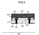
- Fig. 4 is a cross-sectional view of a surface acoustic wave device 900 of a chip size which is a second embodiment of the electronic device in accordance with the present invention.
- the surface acoustic wave device 900 has a structure in which a SAW chip 100 is connected to and sealed on a package substrate 200 by using electroconductive glass 300.
- Internal electrodes 210, external electrodes 220 and through holes 230 for connection between the internal electrodes 210 and the external electrodes 220 are formed on the package substrate 200 in advance.
- the structure shown in Fig. 4 is formed in such a manner that glass balls of several microns are mixed as a spacer in electroconductive glass 300 to control the connection height, thereby ensuring that a space 500 can be formed along the interdigital electrode 110 portion.
- glass rods or electroconductive particles such as Ni balls plated with Au may be used.
- Electroconductive glass 300 electrically connects SAW chip electrodes 120 and the internal electrodes 210 on the package substrate 200 and seals a peripheral portion of the SAW chip 100.
- Fig. 5 is an exploded perspective view of the above-described chip-size surface acoustic wave device 900, showing a state where the SAW chip 100 is removed from the package substrate 200 by cutting at electroconductive glass 300. Electroconductive glass 300 is placed so as to connect signal chip electrodes 121 on the SAW chip 100 and signal internal electrodes 211 on the package substrate 200 and to seal a peripheral portion of the SAW chip 100. A GND chip electrode 122 is connected to a GND internal electrode 212 on the package substrate 200. The GND chip electrode 122 also used for peripheral sealing on the SAW chip 100.
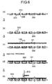
- Figs. 6(a) through 6(e) are diagrams showing the process of assembling the above-described chip-size surface acoustic wave device 900.
- internal electrodes 210, the package substrate 200 on which external electrodes 220 and through holes 230 for connecting these electrodes are formed in advance is prepared.
- a frit for electroconductive glass 300 is printed and molten on the SAW chip mount surface of the above-described package substrate 200 to supply electroconductive glass to the desired position on the package substrate 200.
- a SAW wafer 101 is opposed to and placed on the package substrate 200 on which electroconductive glass 300 is attached, and heating and pressing are performed on the SAW wafer 101 and the package substrate 200 and the package substrate 200 placed one on another.
- Fig. 6(d) shows a connected state after the above-described step.
- the SAW wafer 101 is connected to the chip electrodes 120 and the internal electrodes 210 of the multiple-piece-forming package substrate 200, and peripheral sealing with electroconductive glass 300 is effected on a peripheral portion of each SAW chip.
- the chip-size surface acoustic wave device 900 can be obtained by cutting and separation with a dicer 810 at centers of sealing portions 330 on the multiple-piece-forming package substrate 200.
- Figs. 7(d) through 7(g) are diagrams showing assembly process steps as a modification after the step (d) described with reference to Fig. 6.
- grooving in the direction of mounting of SAW wafer 101 to a depth reaching the package substrate 200 is performed by sandblasting 820 at centers of sealing portions 330 on the multiple-piece-forming package substrate 200 to which the SAW wafer 101 is connected in a sealing manner, thereby separating SAW chips 100.
- the entire back surfaces of the SAW chips 100 including the grooved portions are metalized by evaporation or plating.
- Cu, Ni or Al is used as a metal for this metalization.
- the entire surface may be coated with an electroconductive coating material.
- the grooved portions of the package substrate 200 are broken or cut by dicing to be separated, thereby obtaining individual chip-size surface acoustic wave devices.
- Fig. 8 is a cross-sectional view of a third embodiment of the electronic device in accordance with the present invention.
- portions corresponding to those in Fig. 1 are indicated by the same reference numerals.
- a portion 600 is a shielding member.
- the structure shown in Fig. 8 is formed in such a manner that the chip surface and side surfaces in the structure proposed in the first embodiment are sealed with a shielding member.
- a metallic member or a member surrounded by a metal on the periphery, e.g., a resin member coated with a metal is preferred as the shielding member 600.
- the provision of the shielding member 600 is effective in preventing the influence of electromagnetic waves from other components and in preventing the chip from being chipped by an external force.
- the shielding member 600 can also be used as ground by being connected to the peripheral sealing portion. Further, a heat dissipation effect can be expected.
- the shielding member 600 may be formed, for example, by a method of forming a layer of a resin on the periphery by molding and thereafter plating the surface with a metal, a method of applying a waterproof material or a material containing metal particles by spraying or a method of attaching a metallic cap.
- Fig. 9 is a cross-sectional view of a fourth embodiment of the electronic device in accordance with the present invention.
- a portion 201 is a resin layer
- a portion 202 is a core metal
- a portion 203 is a through hole.
- interdigital electrodes 110, gold bumps 400, chip electrodes 120, a projection 410 for peripheral sealing and a chip electrode 123 for peripheral sealing are provided on a SAW chip 100, and a metal core substrate is formed in such a manner that resin layers 201 are attached to two surfaces of a core metal 202 and wiring is thereafter formed by forming internal electrodes 210, external electrodes 220, an internal electrode 213 for peripheral sealing, tin plating 341, and through holes 203.
- the core metal 202 is made of, for example, a metal such as copper, aluminum or 42 alloy, and the linear expansion coefficient of the metal core substrate can be adjusted by selecting the combination with the number of resin layers 201.
- This embodiment is realized by forming the above-described SAW chip 100 and the metal core substrate by the process shown in Fig. 2, 3 or 7.
- the linear expansion coefficient of the metal core substrate can be adjusted by selecting the combination of core metal 202 and resin layers 201, a package substrate having an extremely small linear expansion coefficient difference from the SAW chip 100 can be formed.
- the stress caused by variation in temperature is thereby limited to improve the reliability of the connection portions.
- the peripheral sealing portion can be provided as a ground terminal by being connected to the core metal 202.
- the core metal 202 can also be used as barrier against electromagnetic waves to prevent the influence of electromagnetic waves from other components.
- Fig. 10 is a cross-sectional view of a fifth embodiment of the electronic device in accordance with the present invention.
- portions corresponding to those in Figs. 8 and 9 are indicated by the same reference numerals.
- a portion 600 is a shielding member.
- the structure shown in Fig. 10 is formed in such a manner that the chip surface and side surfaces in the structure proposed in the fourth embodiment are sealed with a shielding member.
- a metallic member or a member surrounded by a metal on the periphery, e.g., a resin member coated with a metal is preferred as the shielding member 600.
- This embodiment has, in addition to the advantage of the fourth embodiment, the advantage of the provision of the shielding member 600 effective in preventing the influence of electromagnetic waves from other components and in preventing the chip from being chipped by an external force. Since the peripheral sealing portion and the core metal 202 can be connected by the shielding member 600, these members can easily be used as ground. Further, a heat dissipation effect can be expected.
- the shielding member 600 may be formed, for example, by a method of forming a layer of a resin on the periphery by molding and thereafter plating the surface with a metal, a method of applying a waterproof material or a material containing metal particles by spraying or a method of attaching a metallic cap.
- Fig. 11 is a cross-sectional view of a sixth embodiment of the electronic device in accordance with the present invention.
- portions corresponding to those in Fig. 9 are indicated by the same reference numerals.
- a portion 204 is a metalizing on a core metal 202.
- interdigital electrodes 110, gold bumps 400, chip electrodes 120, a projection 410 for peripheral sealing and a chip electrode 123 for peripheral sealing are provided on a SAW chip 100, and a metal core substrate is formed in such a manner that resin layers 201 are attached to two surfaces of a core metal 202 and wiring is thereafter formed by forming internal electrodes 210, external electrodes 220, the metalizing 204, tin plating 341, and through holes 203.
- the core metal 202 is made of, for example, a metal such as copper, aluminum or 42 alloy, and the linear expansion coefficient of the metal core substrate can be adjusted by selecting the combination with the number of resin layers 201.
- the above-described SAW chip 100 and the metal core substrate are formed by the process shown in Fig.
- holes are formed in advance in the resin layers 201 at positions at which the external sealing portion is formed.
- the core metal 202 is thereby exposed. These holes can be formed by laser machining or etching.
- Metalizing 204 is formed in these holes as required and tin plating 341 is further formed. Metalizing 204 is required in a case where it is difficult to form tin plating 341 on the core metal 202.
- a metal for this metalizing is copper, nickel or gold, for example. Positioning between the metal core substrate on which tin plating 341 is formed and the above-described SAW chip 100 is performed and heating and pressing are performed on the metal core substrate and the SAW chip 100, thus realizing this embodiment.
- This embodiment has the advantage of connecting the peripheral sealing portion and the core metal 202 without forming internal wiring in addition to the advantage of the fourth embodiment.
- Fig. 12 is a cross-sectional view of a seventh embodiment of the electronic device in accordance with the present invention.
- portions corresponding to those in Figs. 8 and 9 are indicated by the same reference numerals.
- the structure shown in Fig. 12 is formed in such a manner that the chip surface and side surfaces in the structure proposed in the sixth embodiment are sealed with a shielding member.
- a metallic member or a member surrounded by a metal on the periphery, e.g., a resin member coated with a metal is preferred as the shielding member 600.
- This embodiment has, in addition to the advantage of the sixth embodiment, the advantage of the provision of the shielding member 600 effective in preventing the influence of electromagnetic waves from other components and in preventing the chip from being chipped by an external force.
- the shielding member 600 may be formed, for example, by a method of forming a layer of a resin on the periphery by molding and thereafter plating the surface with a metal, a method of applying a waterproof material or a material containing metal particles by spraying or a method of attaching a metallic cap.
- Fig. 13 is a cross-sectional view of an eighth embodiment of the electronic device in accordance with the present invention.
- portions corresponding to those in Figs. 8 and 9 are indicated by the same reference numerals.
- interdigital electrodes 110, gold bumps 400 and chip electrodes 120 are provided on a SAW chip 100, and a metal core substrate is formed in such a manner that resin layers 201 are attached to two surfaces of a core metal 202 and wiring is thereafter formed by forming internal electrodes 210, external electrodes 220, a metalizing 204, tin plating 341, and through holes 203.
- a shielding member (cap) 600 having gold plating 610 for connection of a shielding material also constitutes the device.
- the core metal 202 is made of, for example, a metal such as copper, aluminum or 42 alloy, and the linear expansion coefficient of the metal core substrate can be adjusted by selecting the combination with the number of resin layers 201.
- a metallic cap or a member surrounded by a metal on the periphery, e.g., a resin cap coated with a metal is preferred as the shielding member 600.
- holes are formed in advance in the resin layers 201 at positions at which the external sealing portion is formed.
- the core metal 202 is thereby exposed. These holes can be formed by laser machining or etching.
- Metalizing 204 is formed in these holes as required and tin plating 341 is further formed.
- Metalizing 204 is required in a case where it is difficult to form tin plating 341 on the core metal 202.
- a metal for this metalizing is copper, nickel or gold, for example.
- the above-described SAW chip 100 and metal core substrate are connected by the process shown in Fig. 2, 3 or 7 and the above-described shielding member 600 is also connected, thus realizing this embodiment.
- a solder may be substituted for the gold plating 610 for connection of the shielding member.
- This embodiment has, in addition to the advantage of the seventh embodiment, the advantage of eliminating the need for the step for peripheral sealing and protection from an external force because connection between the SAW chip 100 and the metal core substrate and cap 600 sealing can be performed at a time.
- Fig. 14 is a cross-sectional view of a ninth embodiment of the electronic device in accordance with the present invention.
- portions corresponding to those in Fig. 8 are indicated by the same reference numerals.
- interdigital electrodes 110, gold bumps 400, a projection 410 for peripheral sealing and chip electrodes 120 are provided on a SAW chip 100, and a flexible substrate 205 having internal electrodes 210, external electrodes 220, metalizing 204, pin plating 341 and through holes 203 is formed.
- tin plating 341 is formed on the internal electrodes 210 and the external electrodes 220 or all pieces of wiring on the device connection surface of the flexible substrate 205 having on its front and back surfaces pieces of wiring, the internal electrodes 210 and the external electrodes 220 formed of copper, for example.
- Metalizing 204 is formed if it is difficult to form tin plating 341 on the wiring, internal electrodes 210 and external electrodes 220.
- Metalizing 204 is formed of nickel or gold, for example. This embodiment is realized by connecting the above-described SAW chip 100 and the flexible substrate 205 by the process shown in Fig. 2 or 3.
- a shielding member 600 may be formed on the periphery as shown in Fig. 8.
- a solder may be substituted for the gold plating 610 for connection of the shielding member.
- This embodiment has, in addition of the advantage of the first embodiment, the advantage that since the rigidity of the flexible substrate 205 is low, the flexible substrate 205 can be deformed to reduce the concentration of stress to the connection portions even when a difference occurs between the amounts of shrinkage of the SAW chip 100 and the flexible substrate 205 due to variation in temperature in an operating environment. Since the flexible substrate is thinner than printed substrates and ceramic substrates, it is possible to provide thinner electronic circuit elements by using the flexible substrate.
- the embodiments 2 to 9 have been described by assuming that the plating material on the internal electrode 213 for peripheral sealing and the internal electrodes 210 on the package substrate 200 is Sn, Ag or Au may be substituted for Sn to effect Au-Ag, Au-Al or Au-Au diffusion bonding between the peripheral sealing chip electrode 123 and the Au bumps on the chip electrodes 120 on the SAW wafer 101. Further, the peripheral sealing portion may be formed so as to surround the interdigital electrodes 110 as shown in Fig. 15.
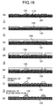
- a method of selectively performing Au plating on the chip electrodes 120 or the peripheral sealing chip electrode 123 on the SAW wafer 101 will be described with respect to the case of plating on the chip electrodes 120 by way of example with reference to Figs. 16(a) through 16(g).
- a SAW wafer on which interdigital electrodes 110 and chip electrodes 120 are formed is prepared.
- film of Cr or Cu is formed as a plating base film 102 on the chip electrode 120 formation surface of the above-described SAW wafer 101 by sputtering or evaporation.
- a plating resist film 103 is formed by spin coating on the SAW wafer 101 on which the plating base film 102 is formed, followed by heating to set the resist film.
- portions of the SAW wafer 101 corresponding to the chip electrodes 120 after application and setting of the plating resist film 103 on the SAW wafer 101 are irradiated with ultraviolet rays and undergo development.
- the resist film 103 is selectively removed at 104 by this patterning.
- electrolytic Au plating 105 is performed on the portions corresponding to the chip electrodes 120, from which the plating resist film 103 has been removed at 104 by patterning.
- the entire plating resist film 103 is removed by using acetone for example.
- the plating base film 102 formed of Cr or Cu is selectively removed by etching using diammonium cerium nitrate so as not to affect Al of the interdigital electrodes 110 and the chip electrodes 120, thus forming the SAW wafer 101 with the desired Au plating pattern.
- an electroconductive glass or a metallic bonding material having low flowability is used as sealing material and the sealing material can therefore be prevented from flowing to the interdigital electrodes even if no flow prevention frame is provided, and a reduction in parts cost and a reduction in assembly cost corresponding to the flow prevention frame can be expected. Also, complete airtight sealing can be achieved to improve the reliability. Further, sealing and electrode connection are performed on the wafer level and individual SAW chip package devices are separated at the final step. Therefore, the device can be reduced to the chip size and can be manufactured in a wafer-size batch process. As a result, remarkable reduction in manufacturing cost can be achieved.
Landscapes
- Engineering & Computer Science (AREA)
- Microelectronics & Electronic Packaging (AREA)
- Manufacturing & Machinery (AREA)
- Physics & Mathematics (AREA)
- Acoustics & Sound (AREA)
- Computer Hardware Design (AREA)
- Surface Acoustic Wave Elements And Circuit Networks Thereof (AREA)
- Wire Bonding (AREA)
Abstract
Description
Claims (9)
- An electronic device comprising a substrate and an electronic circuit element flip-chip-connected on said substrate, wherein a connection is made by gold-tin (Au-Sn) bonding, gold-silver (Au-Ag) bonding, gold-aluminum (Au-Al) bonding or gold-gold (Au-Au) bonding between a chip electrode of said electronic circuit element and an internal electrode on said substrate, and a peripheral portion or a portion which needs to be sealed in said electronic circuit element and said substrate opposed to said electronic circuit element are bonded to each other and sealed by the same method as said bonding method.
- The device of claim 1, wherein said electronic circuit element comprises a piezoelectric element, a SAW chip, a thin film bulk acoustic resonator (FBAR), or a microelectrome-chanical system (MEMS).
- The device of claim 1 or 2, wherein the surface of the electrode on said electronic circuit element is plated with gold (Au) and the surface of the internal electrode on said substrate is plated with tin (Sn), silver (Ag), aluminum (Al) or gold (Au).
- The device of any preceding claim, wherein said substrate comprises a printed substrate, a flexible substrate, a glass substrate, a ceramic substrate, or a silicon substrate.
- A method of manufacturing an electronic device of a chip size, comprising:making a connection by gold-tin (Au-Sn) bonding, gold-silver (Au-Ag) bonding, gold-aluminum (Au-Al) bonding or gold-gold (Au-Au) bonding between an electrode of each of electronic circuit elements each having the electrode and a peripheral portion plated with gold (Au) and the corresponding one of internal electrodes of a multiple-piece-forming substrate on which the internal electrodes and sealing portions plated with tin (Sn), silver (Ag), aluminum (Al) or gold (Au), external electrodes and through hole wiring for connecting the internal and external electrodes are formed, said bonding being performed by heating and pressing the electronic circuit elements and the substrate while opposing the electronic circuit elements and the substrate to each other;sealing the peripheral portion of each of the electronic circuit elements and the sealing portion of the substrate opposed to the peripheral portion of the electronic circuit elements by the same gold-tin (Au-Sn) bonding, gold-silver (Au-Ag) bonding, gold-aluminum (Au-Al) bonding or gold-gold (Au-Au) bonding; andseparating the electronic circuit elements one from another by cutting at the sealing portions to obtain the chip-size electronic device.
- The method of claim 5, further comprising the steps of grooving the sealing portions in the direction of mounting of the electronic circuit elements to a depth reaching the substrate and metalizing the upper surface and the grooved portions before separating the electronic circuit elements one from another by cutting at the sealing portions.
- A method of manufacturing an electronic device, comprising:forming a chromium (Cr) or copper (Cu) film as a plating base film on a surface acoustic wave wafer on which interdigital electrodes and chip electrodes having aluminum (Al) as a major constituent are formed;forming a film of a resist thereon by applying the resist, setting the resist by heating, partially removing the plating resist at positions corresponding to the chip electrodes by irradiation with ultraviolet rays and development;forming a gold plating of a desired thickness on the chip electrode portions;thereafter removing the resist;forming a surface acoustic wave wafer with a gold (Au) plating by selectively removing chromium (Cr) or copper (Cu) forming the plating base film by etching using diammonium cerium nitrate ((CeNH4)2(N3)6) so as not to affect the interdigital electrodes and the chip electrodes having aluminum (Al) as a major constituent; andmanufacturing the electronic device by using the surface acoustic wave wafer and by the method of claim 5 or 6.
- The device or method of any preceding claim, wherein the substrate comprises a metal core substrate.
- The device or method of claim 8, wherein a core metal and a peripheral sealing portion of the metal core substrate are electrically connected to each other.
Applications Claiming Priority (2)
| Application Number | Priority Date | Filing Date | Title |
|---|---|---|---|
| JP2003000789A JP3905041B2 (en) | 2003-01-07 | 2003-01-07 | Electronic device and manufacturing method thereof |
| JP2003000789 | 2003-01-07 |
Publications (2)
| Publication Number | Publication Date |
|---|---|
| EP1445861A2 true EP1445861A2 (en) | 2004-08-11 |
| EP1445861A3 EP1445861A3 (en) | 2009-10-28 |
Family
ID=32652771
Family Applications (1)
| Application Number | Title | Priority Date | Filing Date |
|---|---|---|---|
| EP04000078A Ceased EP1445861A3 (en) | 2003-01-07 | 2004-01-05 | Electronic device and method of manufacturing the same |
Country Status (3)
| Country | Link |
|---|---|
| US (1) | US7211934B2 (en) |
| EP (1) | EP1445861A3 (en) |
| JP (1) | JP3905041B2 (en) |
Cited By (2)
| Publication number | Priority date | Publication date | Assignee | Title |
|---|---|---|---|---|
| US7528529B2 (en) | 2005-10-17 | 2009-05-05 | Semiconductor Energy Laboratory Co., Ltd. | Micro electro mechanical system, semiconductor device, and manufacturing method thereof |
| US8884165B2 (en) | 2008-07-09 | 2014-11-11 | Nec Schott Components Corporation | Packaging device and base member for packaging |
Families Citing this family (57)
| Publication number | Priority date | Publication date | Assignee | Title |
|---|---|---|---|---|
| WO2005099088A1 (en) * | 2004-03-26 | 2005-10-20 | Cypress Semiconductor Corp. | Integrated circuit having one or more conductive devices formed over a saw and/or mems device |
| JP4514562B2 (en) * | 2004-08-26 | 2010-07-28 | 京セラ株式会社 | Surface acoustic wave device and communication device |
| JP4514571B2 (en) * | 2004-09-15 | 2010-07-28 | 京セラ株式会社 | Surface acoustic wave device, method of manufacturing the same, and communication device |
| JP2006086701A (en) * | 2004-09-15 | 2006-03-30 | Kyocera Corp | Surface acoustic wave device, method of manufacturing the same, and communication device |
| JP4514572B2 (en) * | 2004-09-15 | 2010-07-28 | 京セラ株式会社 | Surface acoustic wave device and communication device |
| JP2006050592A (en) * | 2004-07-06 | 2006-02-16 | Matsushita Electric Ind Co Ltd | Piezoelectric resonator and manufacturing method thereof |
| JP4095049B2 (en) * | 2004-08-30 | 2008-06-04 | シャープ株式会社 | High reliability semiconductor device using electrode hermetic sealing |
| JP4583123B2 (en) * | 2004-09-28 | 2010-11-17 | 京セラ株式会社 | High frequency module |
| JP2006210638A (en) * | 2005-01-28 | 2006-08-10 | Sony Corp | Method of manufacturing package structure |
| CN100541767C (en) * | 2005-01-28 | 2009-09-16 | 松下电器产业株式会社 | Method for manufacturing electronic component package and electronic component package |
| JP4699444B2 (en) * | 2005-01-29 | 2011-06-08 | アストリウム・リミテッド | Method for assembling a packaged high frequency circuit module |
| JP4057017B2 (en) | 2005-01-31 | 2008-03-05 | 富士通株式会社 | Electronic device and manufacturing method thereof |
| JP2006245098A (en) | 2005-03-01 | 2006-09-14 | Seiko Epson Corp | Electronic component, manufacturing method thereof, and electronic device |
| JP4692024B2 (en) * | 2005-03-04 | 2011-06-01 | パナソニック株式会社 | Surface acoustic wave device |
| US7362038B1 (en) * | 2005-04-18 | 2008-04-22 | Amkor Technology, Inc. | Surface acoustic wave (SAW) device package and method for packaging a SAW device |
| JP4619201B2 (en) * | 2005-06-01 | 2011-01-26 | 三菱電機株式会社 | Wafer level hermetic package manufacturing method and hermetic package |
| US7316965B2 (en) * | 2005-06-21 | 2008-01-08 | Freescale Semiconductor, Inc. | Substrate contact for a capped MEMS and method of making the substrate contact at the wafer level |
| JP4744213B2 (en) | 2005-07-11 | 2011-08-10 | 日本電波工業株式会社 | Manufacturing method of electronic parts |
| US7419853B2 (en) * | 2005-08-11 | 2008-09-02 | Hymite A/S | Method of fabrication for chip scale package for a micro component |
| FR2890065B1 (en) * | 2005-08-30 | 2007-09-21 | Commissariat Energie Atomique | METHOD FOR ENCAPSULATING A COMPONENT, ESPECIALLY ELECTRIC OR ELECTRONIC, BY MEANS OF AN IMPROVED WELDING CORD |
| JP2007069320A (en) * | 2005-09-08 | 2007-03-22 | Sony Corp | Functional element and manufacturing method thereof |
| JP4770643B2 (en) * | 2005-10-12 | 2011-09-14 | エプソントヨコム株式会社 | Piezoelectric device and manufacturing method thereof |
| US20070120270A1 (en) * | 2005-11-23 | 2007-05-31 | Kuroda Roger T | Flip chip hermetic seal using pre-formed material |
| US7651879B2 (en) * | 2005-12-07 | 2010-01-26 | Honeywell International Inc. | Surface acoustic wave pressure sensors |
| JP4964505B2 (en) * | 2006-06-06 | 2012-07-04 | 株式会社フジクラ | Semiconductor device, manufacturing method thereof, and electronic component |
| JP2008051686A (en) * | 2006-08-25 | 2008-03-06 | Dainippon Printing Co Ltd | Sensor unit and manufacturing method thereof |
| JP2008147427A (en) * | 2006-12-11 | 2008-06-26 | Shinko Electric Ind Co Ltd | Electronic component device and electronic component mounting method |
| JP2008182014A (en) * | 2007-01-24 | 2008-08-07 | Fujikura Ltd | Package substrate and manufacturing method thereof |
| US7954215B2 (en) * | 2007-03-19 | 2011-06-07 | Epson Toyocom Corporation | Method for manufacturing acceleration sensing unit |
| US7564130B1 (en) * | 2007-07-06 | 2009-07-21 | National Semiconductor Corporation | Power micro surface-mount device package |
| JP4661885B2 (en) * | 2008-02-04 | 2011-03-30 | セイコーエプソン株式会社 | Electronic component, manufacturing method thereof, and electronic device |
| JP2009252869A (en) * | 2008-04-03 | 2009-10-29 | Nec Electronics Corp | Method of manufacturing semiconductor device, and semiconductor device manufactured by the method |
| JP5248179B2 (en) * | 2008-04-17 | 2013-07-31 | 新光電気工業株式会社 | Manufacturing method of electronic device |
| US8618670B2 (en) * | 2008-08-15 | 2013-12-31 | Qualcomm Incorporated | Corrosion control of stacked integrated circuits |
| US8138062B2 (en) * | 2009-12-15 | 2012-03-20 | Freescale Semiconductor, Inc. | Electrical coupling of wafer structures |
| EP2553525A1 (en) | 2010-04-01 | 2013-02-06 | Conti Temic Microelectronic GmbH | Device comprising an optical module and support plate |
| TWI420810B (en) | 2010-12-17 | 2013-12-21 | Ind Tech Res Inst | Crystal oscillator and method for manufacturing the same |
| JP2013157483A (en) * | 2012-01-30 | 2013-08-15 | Osaka Univ | Electronic circuit device and method for manufacturing the same |
| JP2014187354A (en) * | 2013-02-21 | 2014-10-02 | Ricoh Co Ltd | Device and method of manufacturing device |
| US9627346B2 (en) * | 2013-12-11 | 2017-04-18 | Taiwan Semiconductor Manufacturing Company, Ltd. | Underfill pattern with gap |
| JP2016206458A (en) * | 2015-04-23 | 2016-12-08 | 株式会社フジクラ | Optical device and method of manufacturing optical device |
| US10580710B2 (en) | 2017-08-31 | 2020-03-03 | Micron Technology, Inc. | Semiconductor device with a protection mechanism and associated systems, devices, and methods |
| JP6635605B2 (en) * | 2017-10-11 | 2020-01-29 | 国立研究開発法人理化学研究所 | Current introduction terminal, pressure holding device and X-ray imaging device having the same |
| US20190157222A1 (en) * | 2017-11-20 | 2019-05-23 | Nxp Usa, Inc. | Package with isolation structure |
| US20190221607A1 (en) * | 2018-01-14 | 2019-07-18 | Innovative Micro Technology | Microfabricated device with piezoelectric substrate and method of manufacture |
| US10381329B1 (en) | 2018-01-24 | 2019-08-13 | Micron Technology, Inc. | Semiconductor device with a layered protection mechanism and associated systems, devices, and methods |
| US10475771B2 (en) | 2018-01-24 | 2019-11-12 | Micron Technology, Inc. | Semiconductor device with an electrically-coupled protection mechanism and associated systems, devices, and methods |
| CN108155287A (en) * | 2018-02-11 | 2018-06-12 | 海宁市瑞宏科技有限公司 | A kind of wafer scale SAWF encapsulating structures with resisting temperature impact effect |
| US11152147B2 (en) * | 2018-02-22 | 2021-10-19 | Samsung Electro-Mechanics Co., Ltd. | Coil component |
| CN109037426B (en) * | 2018-08-10 | 2024-06-14 | 浙江熔城半导体有限公司 | Chip packaging structure with double cofferdams and metal layer and manufacturing method thereof |
| US11476832B2 (en) | 2018-11-30 | 2022-10-18 | Samsung Electro-Mechanics Co., Ltd. | Bulk-acoustic resonator module |
| KR102224307B1 (en) * | 2018-11-30 | 2021-03-08 | 삼성전기주식회사 | bulk-acoustic resonator module |
| US11581870B2 (en) * | 2019-09-27 | 2023-02-14 | Skyworks Solutions, Inc. | Stacked acoustic wave resonator package with laser-drilled VIAS |
| US11244876B2 (en) | 2019-10-09 | 2022-02-08 | Microchip Technology Inc. | Packaged semiconductor die with micro-cavity |
| US20240113066A1 (en) | 2021-02-19 | 2024-04-04 | Sony Semiconductor Solutions Corporation | Electronic device |
| CN119631256A (en) * | 2022-08-02 | 2025-03-14 | 索尼半导体解决方案公司 | Electronic Devices |
| FR3166264A1 (en) * | 2024-09-11 | 2026-03-13 | Vermon | Method for assembling an electroacoustic component to an electronic circuit by reflow soldering |
Citations (3)
| Publication number | Priority date | Publication date | Assignee | Title |
|---|---|---|---|---|
| JPH04293311A (en) | 1991-03-22 | 1992-10-16 | Murata Mfg Co Ltd | Surface acoustic wave device |
| US5705858A (en) * | 1993-04-14 | 1998-01-06 | Nec Corporation | Packaging structure for a hermetically sealed flip chip semiconductor device |
| EP1205970A2 (en) * | 2000-11-10 | 2002-05-15 | Hitachi, Ltd. | Flip chip assembly structure for semiconductor device and method of assembling therefor |
Family Cites Families (28)
| Publication number | Priority date | Publication date | Assignee | Title |
|---|---|---|---|---|
| JPS5478693A (en) * | 1977-12-05 | 1979-06-22 | Matsushima Kogyo Co Ltd | Crystal vibrator |
| CH625372A5 (en) * | 1979-07-06 | 1981-09-15 | Ebauchesfabrik Eta Ag | |
| US4486945A (en) * | 1981-04-21 | 1984-12-11 | Seiichiro Aigoo | Method of manufacturing semiconductor device with plated bump |
| JPS62109420A (en) * | 1985-11-07 | 1987-05-20 | Alps Electric Co Ltd | Surface acoustic wave element |
| JPH0349246A (en) | 1989-07-17 | 1991-03-04 | Hitachi Ltd | Semiconductor integrated circuit device |
| JPH0448733A (en) * | 1990-06-15 | 1992-02-18 | Hitachi Ltd | Multilayer film wiring body, its manufacturing method, and thin film transistor matrix using the same |
| JPH04293310A (en) | 1991-03-22 | 1992-10-16 | Murata Mfg Co Ltd | Surface acoustic wave device |
| JPH05161268A (en) * | 1991-12-02 | 1993-06-25 | Yokogawa Electric Corp | Mounting structure for noise filter |
| JPH0637143A (en) * | 1992-07-15 | 1994-02-10 | Toshiba Corp | Semiconductor device and method of manufacturing semiconductor device |
| JPH0661368A (en) * | 1992-08-05 | 1994-03-04 | Nec Corp | Flip chip type semiconductor device |
| JP2562661Y2 (en) * | 1992-10-13 | 1998-02-16 | 株式会社村田製作所 | Mounting structure of piezoelectric element |
| US5448014A (en) * | 1993-01-27 | 1995-09-05 | Trw Inc. | Mass simultaneous sealing and electrical connection of electronic devices |
| JPH0818390A (en) | 1994-07-01 | 1996-01-19 | Kokusai Electric Co Ltd | Surface acoustic wave device |
| US5864178A (en) * | 1995-01-12 | 1999-01-26 | Kabushiki Kaisha Toshiba | Semiconductor device with improved encapsulating resin |
| JPH08316778A (en) | 1995-05-23 | 1996-11-29 | Mitsumi Electric Co Ltd | Surface acoustic wave device mounting structure |
| JP3380097B2 (en) | 1995-11-01 | 2003-02-24 | 新光電気工業株式会社 | Semiconductor device substrate, method of manufacturing semiconductor device substrate, method of manufacturing semiconductor device using semiconductor device substrate, and semiconductor device |
| JP3683032B2 (en) | 1996-04-22 | 2005-08-17 | 沖電気工業株式会社 | Mounting structure and mounting method of surface acoustic wave device |
| JPH1032223A (en) | 1996-07-15 | 1998-02-03 | Mitsubishi Electric Corp | Semiconductor device |
| JP3284916B2 (en) | 1997-03-12 | 2002-05-27 | 日立電線株式会社 | Semiconductor device and manufacturing method thereof |
| JP3094948B2 (en) * | 1997-05-26 | 2000-10-03 | 日本電気株式会社 | Method of connecting circuit board for mounting semiconductor element and semiconductor element |
| JP3303791B2 (en) * | 1998-09-02 | 2002-07-22 | 株式会社村田製作所 | Electronic component manufacturing method |
| JP3887137B2 (en) * | 1999-01-29 | 2007-02-28 | セイコーインスツル株式会社 | Method for manufacturing piezoelectric vibrator |
| JP2001094390A (en) | 1999-09-20 | 2001-04-06 | Toshiba Corp | Surface acoustic wave device and method of manufacturing the same |
| JP2001110845A (en) | 1999-10-04 | 2001-04-20 | Mitsubishi Electric Corp | Flip chip mounting structure |
| JP4049239B2 (en) * | 2000-08-30 | 2008-02-20 | Tdk株式会社 | Method for manufacturing high-frequency module component including surface acoustic wave element |
| JP2003000789A (en) | 2001-06-21 | 2003-01-07 | Katsuya Seo | Grip assisting glove and assisting belt |
| JP2003078389A (en) | 2001-08-31 | 2003-03-14 | Matsushita Electric Ind Co Ltd | Surface acoustic wave device and method of manufacturing the same |
| JP4766831B2 (en) | 2002-11-26 | 2011-09-07 | 株式会社村田製作所 | Manufacturing method of electronic parts |
-
2003
- 2003-01-07 JP JP2003000789A patent/JP3905041B2/en not_active Expired - Fee Related
-
2004
- 2004-01-05 US US10/750,821 patent/US7211934B2/en not_active Expired - Fee Related
- 2004-01-05 EP EP04000078A patent/EP1445861A3/en not_active Ceased
Patent Citations (3)
| Publication number | Priority date | Publication date | Assignee | Title |
|---|---|---|---|---|
| JPH04293311A (en) | 1991-03-22 | 1992-10-16 | Murata Mfg Co Ltd | Surface acoustic wave device |
| US5705858A (en) * | 1993-04-14 | 1998-01-06 | Nec Corporation | Packaging structure for a hermetically sealed flip chip semiconductor device |
| EP1205970A2 (en) * | 2000-11-10 | 2002-05-15 | Hitachi, Ltd. | Flip chip assembly structure for semiconductor device and method of assembling therefor |
Non-Patent Citations (1)
| Title |
|---|
| WANG C Y ET AL: "An eutectic bonding technology at a temperature below the eutectic point", PROCEEDINGS OF THE ELECTRONIC COMPONENTS AND TECHNOLOGY CONFERENCE. (ECTC). SAN DIEGO, MAY 18 - 20, 1992; [PROCEEDINGS OF THE ELECTRONIC COMPONENTS AND TECHNOLOGY CONFERENCE. (ECTC)], NEW YORK, IEEE, US, vol. CONF. 42, 18 May 1992 (1992-05-18), pages 502 - 507, XP010052575, ISBN: 978-0-7803-0167-2, DOI: 10.1109/ECTC.1992.204252 * |
Cited By (7)
| Publication number | Priority date | Publication date | Assignee | Title |
|---|---|---|---|---|
| US7528529B2 (en) | 2005-10-17 | 2009-05-05 | Semiconductor Energy Laboratory Co., Ltd. | Micro electro mechanical system, semiconductor device, and manufacturing method thereof |
| US8822251B2 (en) | 2005-10-17 | 2014-09-02 | Semiconductor Energy Laboratory Co., Ltd. | Micro electro mechanical system, semiconductor device, and manufacturing method thereof |
| US9054227B2 (en) | 2005-10-17 | 2015-06-09 | Semiconductor Energy Laboratory Co., Ltd. | Micro electro mechanical system, semiconductor device, and manufacturing method thereof |
| US9597933B2 (en) | 2005-10-17 | 2017-03-21 | Semiconductor Energy Laboratory Co., Ltd. | Micro electro mechanical system, semiconductor device, and manufacturing method thereof |
| US10035388B2 (en) | 2005-10-17 | 2018-07-31 | Semiconductor Energy Laboratory Co., Ltd. | Micro electro mechanical system, semiconductor device, and manufacturing method thereof |
| US8884165B2 (en) | 2008-07-09 | 2014-11-11 | Nec Schott Components Corporation | Packaging device and base member for packaging |
| TWI473214B (en) * | 2008-07-09 | 2015-02-11 | 恩益禧肖特電子零件股份有限公司 | Packaging devices and packaging substrates |
Also Published As
| Publication number | Publication date |
|---|---|
| EP1445861A3 (en) | 2009-10-28 |
| JP3905041B2 (en) | 2007-04-18 |
| US20040159960A1 (en) | 2004-08-19 |
| US7211934B2 (en) | 2007-05-01 |
| JP2004214469A (en) | 2004-07-29 |
Similar Documents
| Publication | Publication Date | Title |
|---|---|---|
| US7211934B2 (en) | Electronic device and method of manufacturing the same | |
| CN107919862B (en) | Surface acoustic wave device airtight wafer-level packaging structure and process | |
| US7816794B2 (en) | Electronic device and method of fabricating the same | |
| US7042056B2 (en) | Chip-size package piezoelectric component | |
| JP4766831B2 (en) | Manufacturing method of electronic parts | |
| JP3303791B2 (en) | Electronic component manufacturing method | |
| US7513022B2 (en) | Method for manufacturing surface acoustic wave device | |
| JP4057017B2 (en) | Electronic device and manufacturing method thereof | |
| JP2012151698A (en) | Elastic wave device | |
| JP2009513026A (en) | Semiconductor structure and assembly method | |
| JPH10501102A (en) | Low-cost, high-performance package for microwave circuits in the frequency range up to 90 GHz using BGA I/O RF port format and ceramic substrate technology | |
| WO2008023465A1 (en) | Microelectronic machine mechanism device, and its manufacturing method | |
| KR20030051159A (en) | Semiconductor device | |
| JP4971158B2 (en) | Component device provided with support substrate | |
| JP2012182395A (en) | Electronic device | |
| KR20010020699A (en) | Electronic component | |
| KR20010069987A (en) | Semiconductor Device | |
| KR20060095092A (en) | High Frequency Module Parts and Manufacturing Method Thereof | |
| JP2001110845A (en) | Flip chip mounting structure | |
| JP2006229632A (en) | Surface acoustic wave device | |
| EP1313214A2 (en) | Packaging substrate and manufacturing method thereof, integrated circuit device and manufacturing method thereof, and saw device | |
| JP2006237406A (en) | Resin-sealed electronic component device | |
| JP2007067277A (en) | Electronic device, electronic device manufacturing method, semiconductor wafer | |
| JP2004129193A (en) | Surface acoustic wave device | |
| JP4556637B2 (en) | Functional element body |
Legal Events
| Date | Code | Title | Description |
|---|---|---|---|
| PUAI | Public reference made under article 153(3) epc to a published international application that has entered the european phase |
Free format text: ORIGINAL CODE: 0009012 |
|
| AK | Designated contracting states |
Kind code of ref document: A2 Designated state(s): AT BE BG CH CY CZ DE DK EE ES FI FR GB GR HU IE IT LI LU MC NL PT RO SE SI SK TR |
|
| AX | Request for extension of the european patent |
Extension state: AL LT LV MK |
|
| 17P | Request for examination filed |
Effective date: 20060331 |
|
| RIC1 | Information provided on ipc code assigned before grant |
Ipc: B81B 7/00 20060101ALN20090710BHEP Ipc: H01L 41/053 20060101ALN20090710BHEP Ipc: H03H 3/04 20060101ALN20090710BHEP Ipc: H03H 3/02 20060101ALN20090710BHEP Ipc: H01L 21/60 20060101ALI20090710BHEP Ipc: H01L 23/485 20060101ALI20090710BHEP Ipc: H01L 23/10 20060101ALI20090710BHEP Ipc: H01L 21/50 20060101ALI20090710BHEP Ipc: H03H 9/10 20060101AFI20040507BHEP |
|
| PUAL | Search report despatched |
Free format text: ORIGINAL CODE: 0009013 |
|
| AK | Designated contracting states |
Kind code of ref document: A3 Designated state(s): AT BE BG CH CY CZ DE DK EE ES FI FR GB GR HU IE IT LI LU MC NL PT RO SE SI SK TR |
|
| AX | Request for extension of the european patent |
Extension state: AL LT LV MK |
|
| AKX | Designation fees paid |
Designated state(s): DE GB |
|
| 17Q | First examination report despatched |
Effective date: 20100614 |
|
| STAA | Information on the status of an ep patent application or granted ep patent |
Free format text: STATUS: THE APPLICATION HAS BEEN REFUSED |
|
| 18R | Application refused |
Effective date: 20110929 |