EP1445780A1 - Circuit d'alimentation pour appareil de communication - Google Patents
Circuit d'alimentation pour appareil de communication Download PDFInfo
- Publication number
- EP1445780A1 EP1445780A1 EP03023530A EP03023530A EP1445780A1 EP 1445780 A1 EP1445780 A1 EP 1445780A1 EP 03023530 A EP03023530 A EP 03023530A EP 03023530 A EP03023530 A EP 03023530A EP 1445780 A1 EP1445780 A1 EP 1445780A1
- Authority
- EP
- European Patent Office
- Prior art keywords
- power
- burst period
- transmission
- power amplifier
- voltage
- Prior art date
- Legal status (The legal status is an assumption and is not a legal conclusion. Google has not performed a legal analysis and makes no representation as to the accuracy of the status listed.)
- Granted
Links
- 238000004891 communication Methods 0.000 title claims abstract description 40
- 230000005540 biological transmission Effects 0.000 claims abstract description 226
- 239000003990 capacitor Substances 0.000 claims abstract description 105
- 238000007599 discharging Methods 0.000 claims description 14
- 238000000034 method Methods 0.000 claims description 13
- 230000001934 delay Effects 0.000 claims description 5
- 238000012544 monitoring process Methods 0.000 claims description 4
- 230000000630 rising effect Effects 0.000 claims description 4
- 238000004904 shortening Methods 0.000 abstract description 3
- 230000001413 cellular effect Effects 0.000 description 59
- 238000010586 diagram Methods 0.000 description 29
- 230000007423 decrease Effects 0.000 description 14
- 230000006870 function Effects 0.000 description 12
- 238000012545 processing Methods 0.000 description 8
- 230000001681 protective effect Effects 0.000 description 8
- 230000003321 amplification Effects 0.000 description 6
- 238000006243 chemical reaction Methods 0.000 description 6
- 230000000694 effects Effects 0.000 description 6
- 238000003199 nucleic acid amplification method Methods 0.000 description 6
- 238000004088 simulation Methods 0.000 description 5
- OKTJSMMVPCPJKN-UHFFFAOYSA-N Carbon Chemical compound [C] OKTJSMMVPCPJKN-UHFFFAOYSA-N 0.000 description 4
- 230000009471 action Effects 0.000 description 4
- 230000003247 decreasing effect Effects 0.000 description 4
- 238000001514 detection method Methods 0.000 description 4
- 239000004065 semiconductor Substances 0.000 description 4
- HBBGRARXTFLTSG-UHFFFAOYSA-N Lithium ion Chemical compound [Li+] HBBGRARXTFLTSG-UHFFFAOYSA-N 0.000 description 3
- 238000005516 engineering process Methods 0.000 description 3
- 229910001416 lithium ion Inorganic materials 0.000 description 3
- 230000008859 change Effects 0.000 description 2
- 230000003111 delayed effect Effects 0.000 description 2
- 230000002411 adverse Effects 0.000 description 1
- 229910052782 aluminium Inorganic materials 0.000 description 1
- XAGFODPZIPBFFR-UHFFFAOYSA-N aluminium Chemical compound [Al] XAGFODPZIPBFFR-UHFFFAOYSA-N 0.000 description 1
- 239000003985 ceramic capacitor Substances 0.000 description 1
- 230000008878 coupling Effects 0.000 description 1
- 238000010168 coupling process Methods 0.000 description 1
- 238000005859 coupling reaction Methods 0.000 description 1
- 238000003487 electrochemical reaction Methods 0.000 description 1
- 239000003792 electrolyte Substances 0.000 description 1
- 230000005669 field effect Effects 0.000 description 1
- 238000001914 filtration Methods 0.000 description 1
- 238000010438 heat treatment Methods 0.000 description 1
- 238000004519 manufacturing process Methods 0.000 description 1
- 229910044991 metal oxide Inorganic materials 0.000 description 1
- 150000004706 metal oxides Chemical class 0.000 description 1
- 238000010295 mobile communication Methods 0.000 description 1
- 238000012827 research and development Methods 0.000 description 1
- 230000004044 response Effects 0.000 description 1
- 229910052715 tantalum Inorganic materials 0.000 description 1
- GUVRBAGPIYLISA-UHFFFAOYSA-N tantalum atom Chemical compound [Ta] GUVRBAGPIYLISA-UHFFFAOYSA-N 0.000 description 1
- 238000012546 transfer Methods 0.000 description 1
Images


Classifications
-
- H—ELECTRICITY
- H04—ELECTRIC COMMUNICATION TECHNIQUE
- H04B—TRANSMISSION
- H04B1/00—Details of transmission systems, not covered by a single one of groups H04B3/00 - H04B13/00; Details of transmission systems not characterised by the medium used for transmission
- H04B1/38—Transceivers, i.e. devices in which transmitter and receiver form a structural unit and in which at least one part is used for functions of transmitting and receiving
- H04B1/40—Circuits
-
- H—ELECTRICITY
- H01—ELECTRIC ELEMENTS
- H01G—CAPACITORS; CAPACITORS, RECTIFIERS, DETECTORS, SWITCHING DEVICES, LIGHT-SENSITIVE OR TEMPERATURE-SENSITIVE DEVICES OF THE ELECTROLYTIC TYPE
- H01G11/00—Hybrid capacitors, i.e. capacitors having different positive and negative electrodes; Electric double-layer [EDL] capacitors; Processes for the manufacture thereof or of parts thereof
- H01G11/08—Structural combinations, e.g. assembly or connection, of hybrid or EDL capacitors with other electric components, at least one hybrid or EDL capacitor being the main component
-
- H—ELECTRICITY
- H01—ELECTRIC ELEMENTS
- H01G—CAPACITORS; CAPACITORS, RECTIFIERS, DETECTORS, SWITCHING DEVICES, LIGHT-SENSITIVE OR TEMPERATURE-SENSITIVE DEVICES OF THE ELECTROLYTIC TYPE
- H01G11/00—Hybrid capacitors, i.e. capacitors having different positive and negative electrodes; Electric double-layer [EDL] capacitors; Processes for the manufacture thereof or of parts thereof
- H01G11/14—Arrangements or processes for adjusting or protecting hybrid or EDL capacitors
-
- H—ELECTRICITY
- H02—GENERATION; CONVERSION OR DISTRIBUTION OF ELECTRIC POWER
- H02J—CIRCUIT ARRANGEMENTS OR SYSTEMS FOR SUPPLYING OR DISTRIBUTING ELECTRIC POWER; SYSTEMS FOR STORING ELECTRIC ENERGY
- H02J7/00—Circuit arrangements for charging or depolarising batteries or for supplying loads from batteries
- H02J7/34—Parallel operation in networks using both storage and other dc sources, e.g. providing buffering
- H02J7/345—Parallel operation in networks using both storage and other dc sources, e.g. providing buffering using capacitors as storage or buffering devices
-
- H—ELECTRICITY
- H04—ELECTRIC COMMUNICATION TECHNIQUE
- H04B—TRANSMISSION
- H04B1/00—Details of transmission systems, not covered by a single one of groups H04B3/00 - H04B13/00; Details of transmission systems not characterised by the medium used for transmission
- H04B1/06—Receivers
- H04B1/16—Circuits
- H04B1/1607—Supply circuits
-
- H—ELECTRICITY
- H04—ELECTRIC COMMUNICATION TECHNIQUE
- H04M—TELEPHONIC COMMUNICATION
- H04M19/00—Current supply arrangements for telephone systems
- H04M19/08—Current supply arrangements for telephone systems with current supply sources at the substations
-
- Y—GENERAL TAGGING OF NEW TECHNOLOGICAL DEVELOPMENTS; GENERAL TAGGING OF CROSS-SECTIONAL TECHNOLOGIES SPANNING OVER SEVERAL SECTIONS OF THE IPC; TECHNICAL SUBJECTS COVERED BY FORMER USPC CROSS-REFERENCE ART COLLECTIONS [XRACs] AND DIGESTS
- Y02—TECHNOLOGIES OR APPLICATIONS FOR MITIGATION OR ADAPTATION AGAINST CLIMATE CHANGE
- Y02E—REDUCTION OF GREENHOUSE GAS [GHG] EMISSIONS, RELATED TO ENERGY GENERATION, TRANSMISSION OR DISTRIBUTION
- Y02E60/00—Enabling technologies; Technologies with a potential or indirect contribution to GHG emissions mitigation
- Y02E60/13—Energy storage using capacitors
Definitions
- the present invention relates to a power circuit and a communication device provided with the power circuit and more particularly to the power circuit being suitably used in portable cellular phones or a like employing a TDMA (Time Division Multiple Access) or TDD (Time Division Duplex) communication method and to the communication device provided with the power circuit.
- TDMA Time Division Multiple Access
- TDD Time Division Duplex
- a transmission radio wave since the transmission power amplifier transmits a radio wave, power consumption is large and, during the non-burst period, since a radio wave receiving section of the portable cellular phone receives a radio wave, power consumption is small. Therefore, a load current increases or decreases in a burst manner.
- power for the transmission power amplifier is ordinarily supplied from a battery. The battery discharges in synchronization with a repeating cycle of the burst period and non-burst period.
- the battery supplies power also to internal circuits such as a CPU (Central Processing Unit) or a like in the portable cellular phone, however, if a voltage of the battery becomes below a lower limit value of an operating voltage of the CPU or a like even momentarily, the CPU or a like is put in a frozen state, causing the portable cellular phone to be inoperable. Therefore, whether or not a residual capacity of the battery exists is judged by detecting a lowest voltage value occurring in various operating states and, by setting a somewhat high terminating voltage obtained by providing a margin based on prediction of a momentary heavy loaded state.
- a CPU Central Processing Unit
- the TDMA communication method includes a PDC (Personal Digital Cellular) method being used domestically in Japan, a GSM (Global System for Mobile Communications) and/or GPRS (General Packet Radio Service) methods being used in Europe or a like.
- PDC Personal Digital Cellular
- GSM Global System for Mobile Communications
- GPRS General Packet Radio Service
- Such the conventional portable cellular phone includes a transmission power amplifier 1, a circuit block 2, and a power circuit 3.
- the transmission power amplifier 1 is made up of an amplifier (AMP) 11, a capacitor 12, an amplifier (AMP) 13, a capacitor 14, an amplifier (AMP) 15, and a bias circuit 16.
- Each of the amplifiers 11, 13, and 15 is constructed of a bipolar transistor, a MOS (Metal Oxide Semiconductor) transistor, or a like.
- the bias circuit 16 generates a bias voltage to normally operate these amplifiers 11, 13, and 15.
- each of the transmission power amplifier 1 and circuit block 2 has a lower limit value of an operating voltage required to be operated normally.
- a transmission signal RFIN having a burst period and a non-burst period occurring alternately in a repeated manner, which correspond to the GSM communication method, is input to the amplifier 11.
- the transmission signal RFIN is amplified by the amplifier 11 and an output signal K is then output from the amplifier 11.
- the output signal K after its DC (Direct Current) component has been intercepted by the capacitor 12, is input to the amplifier 13 where it is amplified and is output as an output signal M from the amplifier 13.
- the output signal M, after its DC component has been intercepted by the capacitor 14, is input to the amplifier 15 where it is amplified and a radio wave signal RFOUT as a transmission radio wave from the amplifier 15 is output.
- the circuit block 2 includes various circuits each performing specified operations other than amplifying operations to be performed by the transmission power amplifier 1 using almost constant power to be consumed.
- the various circuits include, for example, a DC-DC converter 21, loads 22 other than the transmission power amplifier 1, or a like, and a lower limit value of a voltage for the specified operations to be performed by each of the various loads 22 is set to be higher than a lower limit value of the voltage for operations to be performed by the transmission power amplifier 1.
- the DC-DC converter 21 boosts or lowers an output voltage of the power circuit 3.
- the loads 22 other than the transmission power amplifier 1 includes, for example, a power source for a microcomputer, a power source for a DSP (Digital Signal Processor), a power source for a SIM (Subscriber Identity Module) card, a power source for a memory, a power source for human interface devices (for example, a voice device, an input / output device, an image pick-up device, or a like) and each of the loads 22 is so configured that an output voltage of the power circuit 3 is directly applied to the loads 22 which can operate at the output voltage of the power circuit 3 and the output voltage of the power circuit 3, after being boosted or lowered by the DC-DC converter 21, is applied to the loads 22 which cannot operate at the output voltage of the power circuit 3 and require conversion of the output voltage.
- a power source for a microcomputer for example, a power source for a DSP (Digital Signal Processor), a power source for a SIM (Subscriber Identity Module) card, a power source for a memory, a power source for human interface devices (for example
- the power circuit 3 is made up of a battery 31, a power management circuit 32, a battery charging circuit 33, and a power bypass condenser 34.
- the battery 31 is a lithium ion battery and is made up of a single cell 35, an internal resistor 36, and a protective circuit 37.
- the power management circuit 32 monitors an output voltage of the battery 31 so as to detect a residual capacity and, when the residual capacity of the battery 31 becomes low and when the output voltage reaches a specified reference level having been set to be more than a lower limit value of an operating voltage of the circuit block 2, produces a control signal to display, for example, an alarm indicating a need for charging to notify a fact that the output voltage of the battery 31 has dropped.
- the battery charging circuit 33 is connected to an outer power source (not shown) charges the battery 31 under specified charging conditions according to a control signal fed from the power management circuit 32.
- the power bypass condenser 34 delays increasing or decreasing of an output current of the battery 31 occurring at the start time or end time of the burst period.
- Figure 16 is a time chart explaining operations of the conventional portable cellular phone shown in Fig. 15.
- Figure 17 is a diagram showing a tolerance of a discharging voltage of the battery 31 shown in Fig. 15, reference for detection of a residual capacity of the battery 31 having been set to the management circuit shown in Fig. 15, a tolerance of an operating voltage of a transmission power amplifier 1 shown in Fig. 15, and a tolerance of an operating voltage of the circuit block 2 shown in Fig. 15.
- An output current of the battery 31 also increases from a current value IBO to a current value IBmax in synchronization with starting of the transmission burst period, however, increasing of the current is delayed due to a surge absorbing action caused by discharging of the power bypass condenser 34. This serves to suppress a fluctuation of an output voltage of the battery 31 caused by starting of the transmission burst period.
- An output voltage of the battery 31, due to an increase of its output current occurring at the start time of the transmission burst period and due to existence of a resistance component by serial connection between the internal resistor 36 and the protective circuit 37, drops by a voltage value ⁇ VBRx ( VB0) from a voltage value VB0 (being equal to an operating voltage VPA0 of the transmission power amplifier 1).
- a current to be consumed remains constant at a level of the current value IPA.
- the output voltage of the battery 31, due to a voltage drop corresponding to an electrostatic capacity component of the battery 31 induced by an output current with the value of IBmax, is lowered by a voltage value ⁇ VBCx ( ⁇ VCx) .
- the current consumed by the transmission power amplifier 1 sharply lowers from the current value IPA to almost 0A.
- the output current of the battery 31 decreases to a level of a current (with a value of IBO) consumed by the circuit block 2 in synchronization with ending of the transmission burst period, however, decreasing of the output current is delayed by the surge absorbing action caused by charging of the power bypass condenser 34. This suppresses a fluctuation of the output voltage of the battery 31 caused by ending of the transmission burst period.
- a current consumed by the transmission power amplifier 1 is almost 0A.
- this voltage value VB1 becomes below a lower limit value of an operating voltage of the internal circuit such as the CPU in the portable cellular phone even momentarily, since the portable cellular phone becomes inoperable, a residual life of the battery 31 is judged based on this voltage value VB1.
- a voltage value ⁇ VBx that can be obtained by simulation using following conditions becomes about 300 mV.
- the output of the battery 31 is, for example, 3. 5 V during the receiving non-burst period, it becomes 3. 2 V or less during the transmission burst period and, since it reaches the level that an alarm indicating a need for charging is issued according to the reference for detection of a residual capacity of the battery 31 shown in Fig. 17, a notification is provided by the power management circuit 32 informing that the output of the battery 31 has dropped.
- a tolerance of an operating voltage of the transmission power amplifier 1 is 4.2 V to 2.7 V
- a tolerance of an operating voltage of the circuit block 2 is 4.2 V to 3.0 V and there is a difference of about 0.3 V ( ⁇ VM) in the lower limit values in the operating voltage between the transmission power amplifier 1 and the circuit block 2.
- ⁇ VM 0.3 V
- a radio communication device as one of examples of the technology described above is disclosed in Japanese Patent Application Laid-open No. Hei 04-315320, in which a capacitor is charged by a battery to have a voltage of 10 V using a voltage boosting device and, during a transmission burst period, a switching unit is closed to allow power to be applied by the capacitor to a power amplifier. At this point, a burst signal is amplified by the power amplifier and is transmitted and, during a non-burst period, a switching unit is opened to allow the capacitor to be charged.
- the switching unit is closed during the transmission burst period and is opened during the non-burst period, however, such the method in which the capacitor is charged at an idle slot time during the non-transmission period (non-burst period) can be employed only in a device in which transmission time is comparatively short (its duty ratio being about 1/8). That is, as a ratio of transmission time becomes larger, the capacitor has to be charged in a shorter time and, when this ratio exceeds 50%, the switching unit produces an adverse effect.
- functions of the portable cellular phone tend to be expanded, that is, although the conventional function is to perform only voice speech, a recent function includes transmission of data. In the portable cellular phone of the TDMA type, such the expansion of the functions causes transmission slots to increase and the ratio of transmission time to rise and, therefore, the switching unit is not effective in achieving long-time speech in the portable cellular phone.
- the voltage boosting device is a DC-DC converter made up of a coil, resistor, semiconductor, or a like
- the switching unit is made up of a mechanical switching element or a semiconductor switching element
- the capacitor is about 100 mm 3 in size. If all these components are housed in the portable cellular phone, the portable cellular phone becomes very large and heavy, thus impairing a portability characteristic of the portable cellular phone.
- a power circuit to be used in a communication device including a transmission power amplifier to amplify a transmission signal having a burst period and a non-burst period occurring alternately in a repeated manner, the power circuit including:
- a communication device including:
- a power circuit to be used in a communication device including a transmission power amplifier to amplify a transmission signal having a burst period and a non-burst period occurring alternately in a repeated manner and with a load circuit to consume power required for performing operations, the power circuit including:
- a communication device including:
- a preferable mode is one wherein the transmission power amplifier has a lower limit value of a first operating voltage to normally operate the transmission power amplifier, the load circuit has a lower limit value of a second operating voltage to normally operate the load circuit, the lower limit value of the second operating voltage is set to be higher than the lower limit value of the first operating voltage, the reference level is set to be not less than the lower limit value of the second operating voltage, and the power supplying unit is made up of a battery or a direct current power source in which in which an upper limit value is imposed on a current to be output therefrom.
- a preferable mode is one wherein the power storing section is so configured as to be charged, when a voltage of the power storing section becomes lower than that of the power supplying unit during the burst period, until a voltage of the power storing section becomes almost equal to a voltage of the power supplying unit during the non-burst period occurring subsequent to the burst period.
- Another preferable mode is one that wherein further includes:
- Still another preferable mode is one wherein the control circuit controls the first power to be fed from the power supplying unit to the transmission power amplifier, by controlling an output current of the control circuit, the output current being fed from the power supplying unit to the transmission power amplifier.
- a further preferable mode is one wherein the output current of the control circuit is set to have a current value such that almost all amount of power needed to be consumed by the transmission power amplifier during one frame period being made up of one burst period and one non-burst period may be supplied to the transmission power amplifier.
- An additional preferable mode is one wherein the power storing unit supplies the second power to the transmission power amplifier by discharging when power needed to be consumed by the transmission power amplifier during the burst period is larger than the first power being supplied under control of the control circuit, and wherein the control circuit exerts control so that the power storing section having discharged during the burst period is charged to accumulate redundancy of the first power as the second power when power to be consumed by the transmission power amplifier during the non-burst period is smaller than the first power being supplied under control of the control circuit.
- still additional preferable mode is one wherein the delay device delays a rising and falling of an output current of the power supplying unit at time of start and end of the burst period.
- a further preferable mode is one wherein the power storing section is made up of an electrical double layer capacitor.
- the electrical double layer capacitor has unit cells constructed as a capacitor of sheet-shaped electrical double layer structure which make up stacked cells in which arbitrary numbers of the unit cells are stacked in layer so as to be able to provide a specified withstand voltage and electrostatic capacity.
- Another preferable mode is one wherein the transmission signal is transmitted by a TDMA (Time Division Multiple Access) or TDD (Time Division Duplex) communication method.
- TDMA Time Division Multiple Access
- TDD Time Division Duplex
- the electrical double layer capacitor serving as the power storing section is made up of thin-sheet-shaped unit cells and is so constructed in a manner that a plurality of the unit cells are stacked in layer, the power circuit can be made thin, which enables mounting of the power circuit of the present invention suitably on a folding-type portable cellular phone without causing an increase in a thickness of a case of the portable cellular phone.
- the power circuit of the present invention does not use such the voltage boosting unit as disclosed in Japanese Patent Application Laid-open No. Hei 4-315320 and, therefore, no case occurs in which an operating voltage of the transmission power amplifier is higher than a voltage to be supplied by the power supplying unit.
- the power circuit of the present invention is equipped with the control circuit to limit an output current fed from the power supplying unit to a pre-set upper limit current value, irrespective of transmitting and receiving timing in the TDMA-type or TDD -type communication system and, therefore, no effects decrease due to an increase in a ratio of transmission time.
- the power circuit of the present invention includes the control circuit, the delay device made up of a capacitor, and power storing section having an electrical double layer capacitor, in which the capacitor and control circuit are constructed so as to be of surface mounting type and the electrical double layer capacitor is formed to be of a thin shape and, therefore, mounting of the power circuit on the folding-type portable cellular phone can be can be achieved without an increase in thickness of the folding-type portable cellular phone being presently a mainstream.
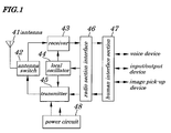
- FIG. 1 is a schematic block diagram showing electrical configurations of a communication device being equipped with a power circuit of a first embodiment of the present invention.
- the communication device of the first embodiment is a portable cellular phone and includes an antenna 41, an antenna switch 42, a receiver 43, a local oscillator 44, a transmitter 45, a radio section interface 46, a human interface section 47, and a power circuit 48.
- the antenna 41 is used to transmit and receive a radio wave to and from a radio base station (not shown) and its length is set based on a wavelength of a radio wave to be used for communication.
- the antenna switch 42 selects either the receiver 43 or the transmitter 45 to establish connection to the antenna 41.
- the receiver 43 performs amplification and/or frequency conversion of a received signal, or a like.
- the local oscillator 44 generates a signal having a reference frequency required for frequency conversion of a received signal or a transmitting signal by a control signal of the radio section interface 46.
- the transmitter 45 makes a frequency conversion of and/or performs amplification on a transmitting signal.
- the radio section interface 46 encodes a received signal or a transmitting signal, transmits encoded signals to the human interface section 47, and controls the local oscillator 44 all the time.
- the human interface section 47 is connected to analog input / output devices including a voice device such as a speaker, microphone, or a like (not shown) , an input / output device such as a keyboard, display, or a like (not shown) , an image pick-up device such as a camera (not shown) , and serves as a mediator between a user and the portable cellular phone.
- the power circuit 48 supplies power to each of the above components.
- the antenna 41 is connected to the receiver 43 through the antenna switch 42.
- the radio wave received by the antenna 41 is amplified by the receiver 43, and its frequencies is further down-converted by a signal fed from the local oscillator 44.
- the received wave of which frequency were down-converted is then transmitted to the radio section interface 46.
- the received wave is demodulated and decoded by the radio section interface 46 and is further transmitted to a user through the human interface section 47.
- the antenna 41 is connected to the transmitter 45 through the antenna switch 42.
- the user inputs information that the user wants to transfer to a destination as a voice, character, or image using a microphone, keyboard, camera, or a like being connected to the human interface section 47.
- the input information is transmitted to the radio section interface 46 where encoding and/or modulation are performed and is then transmitted to the transmitter 45.
- a transmitting signal is up-converted to become a high- frequency wave by a signal fed from the local oscillator 44 and is then amplified and transmitted as a radio wave through the antenna switch 42 from the antenna 41.
- FIG. 2 is a diagram showing the antenna 41, antenna switch 42, local oscillator 44, transmitter 45, radio section interface 46, and human interface section 47, which are all taken from Fig. 1, and illustrates electrical configurations of main components of the transmitter 45 and radio section interface 46.
- the radio section interface 46 as shown in Fig. 2, is made up of a signal processing section 51 and an intermediate frequency (IF) wave section 52.
- the signal processing section 51 is made up of a DSP (Digital Signal Processor) or a like and performs digital signal processing such as filtering on data to be transmitted (voice signal, image signal, or a like) output from the human interface section 47.
- the intermediate frequency wave section 52 performs modulation and intermediate frequency wave amplification on a signal output from the signal processing section 51.
- the transmitter 45 includes a band-pass filter 53, a mixer (MIX) 54, a band-pass filter 55, a buffer (BUFF) 56, and a transmission power amplifier 57.
- the band-pass filter 53 eliminates noises contained in a transmitting signal fed from the intermediate frequency wave section 52.
- the mixer 54 up-converts a frequency of the transmitting signal to become a high frequency wave by using a reference frequency fed from the local oscillator 44.
- the band-pass filter 55 eliminates noises contained in the transmitting signal fed from the mixer 54.
- the buffer 56 receives the signal having been up-converted to be a high frequency wave at high input impedance and transmits the signal at low output impedance to the transmission power amplifier 57.
- the transmission power amplifier 57 performs power amplification on the signal fed from the buffer 56 to use the signal as a transmission radio wave.
- "data to be transmitted" output from the human interface section 47 is input to the signal processing section 51 in which digital signal processing is performed on the "data to be transmitted” and is then modulated by the intermediate frequency wave section 52 in which amplification is performed on an intermediate frequency wave and is output as a transmitting signal.
- Noises contained in the transmitting signal, which have occurred at the time of the amplification performed on the intermediate frequency wave, are removed by the band-pass filter 53 in the transmitter 45.
- the transmitting signal output from the band-pass filter 53 receives a reference frequency fed from the local oscillator 44 in the mixer 54 and its frequency is up-converted to become a high frequency wave.
- the transmitting signal fed from the band-pass filter 55 is output through the buffer 56 to the transmission power amplifier 57.
- the signal sent out from the buffer 56 is power-amplified by the transmission power amplifier 57 and is transmitted through the antenna switch 42 from the antenna 41 as a radio wave.
- FIG. 3 is a circuit diagram for showing electrical configurations of main components of the power circuit 48 shown in Fig. 1, the transmission power amplifier 57 shown in Fig. 3, and a circuit block 58.
- the transmission power amplifier 57 as shown in Fig. 3, includes an amplifier (AMP) 71, a capacitor 72, an amplifier (AMP) 73, a capacitor 74, an amplifier (AMP) 75, and a bias circuit 76.
- Each of the amplifiers 71, 73, and 75 is made up of a bipolar transistor, MOS transistor, or a like.
- the bias circuit 76 generates a bias voltage used to normally operate these amplifiers 71, 73, and 75.
- Each of the transmission power amplifier 57 and the circuit block 58 has a lower limit value of an operating voltage for its normal operations.
- a transmission signal RFIN to be employed in the TDMA communication method (for example, GSM method) in which a burst period and a non-burst period occur alternately in a repeated manner or to the TDD communication method is input to the amplifier 71.
- the transmission signal RFIN is amplified by the amplifier 71 from which an output signal K is output.
- the output signal K fed from the amplifier 71 after its DC (Direct Current) component has been intercepted by the capacitor 72, is input to the amplifier 73 where it is amplified and is then output as an output signal M from the amplifier 73.
- the output signal M after its DC component has been intercepted by the capacitor 74, is input to the amplifier 75 where it is amplified and a radio signal RFOUT as a transmission radio wave is output from the amplifier 75.
- the circuit block 58 includes various circuits other than the transmission power amplifier 57 shown in Fig. 2 and is made up of, for example, a DC-DC converter circuit 81 and loads 82 other than the transmission power amplifier 57 and provides a tolerance of an operating voltage having a lowest limit value being higher than that of an operating voltage of the transmission power amplifier 57 and consumes power required for operational processing.
- the DC-DC converter circuit 81 boosts or lowers an output voltage of the power circuit 48.
- the loads 82 other than the transmission power amplifier 57 are made up of, for example, power sources for a microcomputer, DSP, SIM card, memory, human interface devices (for example, a voice device, input / output device, image pick-up device or a like) in which the output voltage of the power circuit 48 is directly applied to loads 82 other than the transmission power amplifier 57 that operate at the output voltage of the power circuit 48 and a voltage obtained by boosting or lowering the output voltage of the power circuit 48 using the DC-DC converter circuit 81 is applied to those that do not operate at the output voltage of the power circuit 48 and require conversion of voltages.
- power sources for a microcomputer, DSP, SIM card, memory, human interface devices for example, a voice device, input / output device, image pick-up device or a like
- the power circuit 48 is made up of a battery 59, a power management circuit 60, a battery charging circuit 61, and a circuit mounting section 65.
- the circuit mounting section 65 includes a control circuit 63, an input capacitor 62 as a delay device, and an electrical double layer capacitor 64.
- the battery 59 is, for example, a lithium ion battery and its discharging voltage range is generally from about 4.2 V to about 2.5 V.
- the battery 59 includes a single cell 91, an internal resistor 92, and a protective circuit 93 and a resistance of the internal resistor 92 is produced by an electrolyte and a combined resistance including electrode connecting resistance and/or charge movement resistance, or a like.
- the protective circuit 93 is made up of a transistor, thermistor, or a like and detects occurrence of overcharge, over-discharge, over-current, heating, or a like and insulates the battery 59 from loads.
- the power management circuit 60 monitors an output voltage of the battery 59 and detects a residual capacity according to a reference for detection employed in the conventional technology shown in Fig. 17 and, when the residual capacity becomes small and the output voltage becomes a specified level of reference having been set to be more than a lower limit value of an operating voltage of the circuit block 58, a notification informing that the output voltage has dropped is provided by producing a control signal, for example, to display an alarm for charging.
- a control signal for example, to display an alarm for charging.
- the output voltage of the battery 59 is, for example, about 4. 2 V
- a residual capacity is at a full charge level and the battery 59 has a voltage enough to drive the transmission power amplifier 57 and the circuit block 58.
- the output voltage of the battery 59 is, for example, about 3.
- the residual capacity is at an intermediate level and the battery 59 has a voltage enough to drive the transmission power amplifier 57 and the circuit block 58.
- the output voltage of the battery 59 is, for example, about 3.2 V
- the residual capacity is at a level that an alarm indicates a need for charging.
- the battery 59 has a voltage enough to drive the transmission power amplifier 57
- the output voltage of the circuit block 58 has reached a lower limit value (3.0 V) of tolerance of the output voltage of the circuit block 58, a state in which an operating voltage is in short supply occurs.
- the voltage of 3.2 V is set as a terminating voltage for the battery 59.
- the battery charging circuit 61 by being connected to an outside power source not shown, charges the battery 59 at a specified voltage and at a specified current based on a control signal fed from the power management circuit 60.
- the input capacitor 62 is charged or discharged when a current to be consumed by the transmission power amplifier 57 rapidly increases (rises up) or decreases (falls down) , and delays a rising edge or a falling edge of an output current of the battery 59 occurring at a rise time or a fall time of the burst period.
- the control circuit 63 is made up of a p-channel MOSFET (Metal-Oxide-Semiconductor Field Effect Transistor) (hereafter called simply as a "pMOS”) 101, a gate control block 102, and a current control block 103.
- the current control block 103 detects a drain current based on a voltage between a drain and a source of the pMOS 101 and transmits a control signal C to the gate control block 102 so that the drain current becomes a pre-set value.
- the gate control block 102 based on the control signal C, produces a gate control voltage G used to control a resistance value between the drain and source of the pMOS 101.
- a resistance between the drain and source is controlled based on the gate control voltage G and a drain current based on the resistance flows.
- the control circuit 63 feeds an output current being limited to a pre-set current value from the battery 59 to the transmission power amplifier 57 and, when a voltage of the electrical double layer capacitor 64 becomes below a voltage of the battery 59 during the burst period, charges the electrical double layer capacitor 64 during the subsequent non-burst period until a voltage of the electrical double layer capacitor 64 becomes almost equal to a voltage of the battery 59.
- an output current (drain current of the pMOS 101) of the control circuit 63 is set to be a current value that can supply almost all power being able to be consumed in one frame cycle made up of one burst period and one non-burst period to the transmission power amplifier 57.
- the one frame cycle is several milliseconds. Furthermore, the control circuit 63, when power to be consumed in the transmission power amplifier 57 during the non-burst period is smaller than power that the control circuit 63 can supply, charges the electrical double layer capacitor 64 that has discharged during the burst period.
- the electrical double layer capacitor 64 is made up of, for example, an electrostatic capacitor 111 and an internal resistor 112 and is charged by an output current of the control circuit 63 and accumulates power to feed it to the control circuit 63 and the transmission power amplifier 57.
- the electrostatic capacitor 111 has capacitance of a few tens of mF or more and the internal resistor 112 has resistance of 500 m ⁇ or less.
- the electrical double layer capacitor 64 when power to be consumed by the transmission power amplifier 57 during the burst period is larger than power that can be supplied by the control circuit 63, feeds power for replenishing by discharging.
- the circuit mounting section 65 includes the input capacitor 62, control circuit 63, and electrical double layer capacitor 64, in which a power source terminal 313 and a ground terminal 314 are mounted on an input side and a power source terminal 311 and a ground terminal 312 are mounted on an output side.
- FIG. 4 is a diagram showing configurations of a circuit mounting section 65 shown in Fig. 3.
- the circuit mounting section 65 is made of a flexible printed circuit board (FPC board) for example in which the input capacitor 62 constructed so as to be of surface mounting type and the control circuit 63 are mounted and, since the electrical double layer capacitor 64 is mounted to one terminal of the circuit mounting section 65, its thickness is 2 mm or less and a product of a length and a width is about 200 mm 2 .
- FPC board flexible printed circuit board
- FIG. 5 is a diagram showing configurations of the electrical double layer capacitor 64 shown in Fig. 4.
- the electrical double layer capacitor 64 as shown in Fig. 5, includes six pieces of unit cells 121 having a structure of double-layers made of thin sheets in which these units cells 121 are stacked in layer which make up a stacked cell 122 that can provide a withstand voltage and electrostatic capacity required as a power source for the transmission power amplifier 57. Also, at an end portion of the unit cell 121 placed on an uppermost portion is mounted a positive electrode 123 and at an end of the unit cell 121 placed on a lowermost portion is mounted a negative electrode 124. The stacked cell 122 is sandwiched between the insulating films 125 in a manner that the positive electrode 123 and the negative electrode 124 are exposed.
- FIG. 6 is a diagram showing configurations of the unit cell 121 shown in Fig. 5.
- the unit cell 121 as shown in Fig. 6, is made up of a current collector 131, a separator 132, an activated carbon layer 133, and a gasket 134.
- the current collector 131 serves as a positive pole or a negative pole and the separator 132 separates the positive pole from the negative pole.
- the activated carbon layer 133 accumulates a charge and is held by the gasket 134.
- a capacitor is constructed based on a principle of a thin-sheet-shaped electrical double layer.
- the electrical double layer capacitor 64 has an electrostatic capacity being larger than that of a ceramic capacitor, aluminum electrolytic capacitor, tantalum electrolytic capacitor, or a like, and its electrostatic capacitor has for example a product of a length and a width being about 1000 mm 2 , a thickness being about 2 mm, capacity of 30 mF or more (withstand voltage: for example, 5V).
- an effective dimension of a clearance between an outer case and a component mounting portion in presently- available portable cellular phones is 2 mm or so in height and about 1500 mm 2 in area and, since a clearance that can be formed by the circuit mounting section 65 and electrical double layer capacitor 64 of the embodiment can fall within the above effective dimension employed in the presently-available portable cellular phones, mounting of a power circuit in the portable cellular phone can be achieved, without impairing portability of portable cellular phones, by using the circuit mounting section 65 and electrical double layer capacitor 64 of the embodiment of the present invention.
- Figure 7 is a time chart explaining operations of the power circuit 48 and the transmission power amplifier 57 shown in Fig. 3.
- Figure 8 is a diagram explaining an effect of lengthening a life of the battery 59 according to the first embodiment of the present invention.
- Figure 9 is also a diagram explaining the effect of lengthening the life of the battery 59 according to the first embodiment of the present invention. Operations of the portable cellular phone of the first embodiment are described by referring to Figs. 7, 8, and 9.
- a current consumed by the transmission power amplifier 57 rapidly increases from 0A to a current value IPA.
- a discharging current IDCG is fed from the electrical double layer capacitor 64 to the transmission power amplifier 57.
- a current output from the battery 59 increases, in synchronization with starting of the transmission burst period, up to a current value IBmax being an upper limit value set by the control circuit 63, however, there is a delay in the increase of the output current of the battery 59 by an action of absorbing a surge caused by discharging of the input capacitor 62. This serves to suppress a fluctuation of the output voltage of the battery 59 due to the start of the transmission burst period.
- the current with the value IDCG of the electrical double layer capacitor 64 is combined with the current with the value IBmax of the battery 59 and the combined current is fed as a current value IPA to the transmission power amplifier 57.
- a voltage being applied from the electrical double layer capacitor 64 to the transmission power amplifier 57 drops by a voltage value ⁇ VRy from a voltage value VPA0 induced by a voltage drop determined by resistance of the internal resistor 112 and an amount of a discharged current of the electrical double layer capacitor 64, in synchronization with starting of the transmission burst period.
- An output voltage of the battery 59 drops due to existence of a resistance component in series between the internal resistor 92 and the protective circuit 93 and lowers from a voltage value VB0 by a voltage value ⁇ VBRy.
- a consumed current remains constant at a level of the current value IPA.
- a discharging current (current with a value of IDCG) fed from the electrical double layer capacitor 64 is continuously fed to the transmission power amplifier 57.
- the output current of the battery 59 after the delay caused by the input capacitor 62 has disappeared, remains at a level of the current value IBmax set by the control circuit 63.
- a voltage being applied to the transmission power amplifier 57 from the electrical double layer capacitor 64 is lowered by a voltage value ⁇ VCy due to a voltage drop caused by discharging of the electrical double layer capacitor 64.
- the output voltage of the battery 59 due to a voltage drop corresponding to an electrostatic capacity component of the battery 59 induced by an output current with the value of IBmax, lowers by a voltage value obtained by adding a voltage value ⁇ VBCy to a decrease ⁇ VBRy of a voltage value at the time t0.
- a voltage being applied from the electrical double layer capacitor 64 to the transmission power amplifier 57 is boosted by a voltage value ⁇ VRy from a voltage with a value of VPA1 in synchronization with ending (falling edge) of the transmission burst period in response to an increase in voltage determined by a resistance of the internal resistor 112 in the electrical double layer capacitor 64 and by an amount of a charged current of the electrical double layer capacitor 64. Due to a voltage drop being equivalent to a voltage value ⁇ VBRy occurring at the time t0 and due to an additional voltage drop corresponding to an electrostatic capacity component of the battery 59 induced by an output current with the value of IBmax, the output voltage of the battery 59 has further lowered.
- a voltage being applied from the electrical double layer capacitor 64 to the transmission power amplifier 57 is gradually boosted since the electrical double layer capacitor 64 is charged at a current being smaller than the current value ICHG.
- the output voltage of the battery 59 is gradually boosted since the output current of the battery 59 is limited due to existence of a resistance component by serial connection between the internal resistor 92 and the protective circuit 93.
- the output voltage of the battery 59, as its output current decreases, is boosted exponentially based on a time constant of an electrostatic capacity and a resistance component of the battery 59.
- the output voltage of the battery 59 remains commensurate in voltage with a current with the value of IB0 to be fed to the circuit block 58. Then, these voltages and currents are again put into the state that has occurred at the time t0 and, thereafter, same operations are repeated in order of the time t0, period T1, time t1, period T2, time t2,period T3, time t3, period T0, time t0, ⁇ .
- a life of the battery 59 is judged based on a lowest voltage value VB1 occurring during the transmission burst period.
- a simulation value of the voltage value ⁇ VBy used to obtain the above voltage value VB1 becomes about 90 mV being one third or less of a conventional value of 300 mV.
- the output of the battery 59 does not become 3.2 V or less (terminating voltage) during the transmission burst period until it becomes 3.3 V during the receiving non-burst period, the battery 59 is usable until its output voltage becomes lower than that in the conventional case and its life can be lengthened.
- a life of the battery 59 being put at ambient temperature being at room temperature of about 20°C is described by referring to Fig. 8.
- the curve "B” shows movement of the voltage value VB1 of the battery 59 occurring at the time t2 shown in Fig. 7.
- the dotted-line curve D shows movement of an operating voltage VPA1 of the transmission power amplifier 57 occurring at the time t1 shown in Fig. 7.
- the output voltage of the battery 31 occurring during the transmission burst period moves as shown by the broken-line curve C and, at the time L1, the life of the battery 31 is judged to have been over.
- the output voltage of the battery 59 occurring during the transmission burst period moves as shown in the curve B and, at the time of L2, the life of the battery 59 is judged to have been over and the life of the battery 59 being longer than that of the battery 31 can be provided.
- a life of the battery 59 being put at ambient temperature being below 0°C is described by referring to Fig. 9.
- a battery operating by an electrochemical reaction its internal resistance increases with a decrease of ambient temperatures. Therefore, an output voltage of the battery is lowered with an increase in internal resistance.
- a terminating voltage of a battery 31 being set in the power management circuit 60, as shown in Fig. 9, is set to be constant irrespective of ambient temperatures and, therefore, in a low-temperature environment, a life of the battery 31 is remarkably shortened.
- an output voltage of the battery 31 being put in a low-temperature occurring during the transmission burst period moves as shown in the broken-line curve C and, at the time L1LT, the life of the battery 31 is judged to have been over and is remarkably shortened compared with a case where the battery is put at room temperature.
- an output voltage of the battery 59 occurring during the transmission burst period, as shown by the curve B since a voltage drop is small during the transmission burst period, at the time L2LT, the life of the battery 59 is judged to have been over and the life is not shortened extremely unlike in the case of the battery 31.
- the electrical double layer capacitor 64 is so constructed as to have thin-sheet shaped unit cells 121 and so that these unit cells 121 are stacked in layer, it can be mounted on a folding-type portable cellular phone without causing an increase in thickness.
- FIG. 10 is a schematic block diagram showing electrical configurations of a portable cellular phone according to a second embodiment of the present invention.
- same reference numbers are assigned to corresponding parts having same functions as the first embodiment shown in Fig. 1.
- the portable cellular phone of the embodiment has, instead of a radio section interface 46 and a human interface section 47 employed in the first embodiment shown in Fig. 1, a radio section interface 46A and human interface section 47A to each of which new functions are added and further newly includes a PDA (Personal Digital Assistance) functional block 141.
- PDA Personal Digital Assistance
- an operating system (OS) is mounted and software is installed.
- OS operating system
- Each of the radio section interface 46A and human interface section 47A in addition of the functions of the radio section interface 46 and the human interface section 47A employed in the first embodiment, has a function of swapping specified data with the PDA functional block 141.
- Other components shown in Fig. 10 have the same functions as the first embodiment shown in Fig. 1.
- the portable cellular phone of the second embodiment performs, in addition to operations performed by the portable cellular phone of the first embodiment, operations of, for example, scheduling management and computation.
- FIG 11 is a schematic block diagram showing electrical configurations of a portable cellular phone according to a third embodiment of the present invention.
- the portable cellular phone of the third embodiment has, instead of a human interface 47 shown in Fig. 1, a digital interface 142.
- the digital interface 142 is connected through, for example, a USB (Universal Serial Bus) port or a PC (Personal Computer) card slot to a personal computer 143.
- the PC card slot adheres to the PCMCIA (Personal Computer Memorycard International Association).
- PCMCIA Personal Computer Memorycard International Association
- the portable cellular phone of the third embodiment in ordinary cases, power is supplied from the personal computer 143 and, if the personal computer 143 is, for example, a battery-driven notebook PC, by using a power circuit 48, communications time according to the TDMA- system can be extended.
- a power source such as a USB-type bus power source in which a limitation is imposed on an output current is employed as a power source for a transmitter 45
- a power source current exceeds the limited power source current during a transmission burst period at the time of communications which impairs normal communications.
- an amount of the power source current during the transmission burst period is reduced, thus enabling smooth communications.
- Figure 12 is a diagram illustrating configurations of a circuit mounting section 65A of a power circuit according to a fourth embodiment of the present invention.
- same reference numbers are assigned to corresponding parts having same functions as the first embodiment shown in Fig. 1.
- the circuit mounting section 65A is placed instead of the circuit mounting section 65 shown in Fig. 3 and has electrical double layer capacitors 64A and 64B on its both sides. To obtain specified electrical characteristics, these electrical double layer capacitors 64A and 64B are connected to each other serially or in parallel.
- FIG 13 is a diagram illustrating configurations of a circuit mounting section 65B in a power circuit according to a fifth embodiment of the present invention.
- an electrical double layer capacitor 64C is mounted on one end of the circuit mounting section 65B.
- Figure 14 is a diagram illustrating configurations of the electrical double layer capacitor 64C of Fig. 13.
- the electrical double layer capacitor 64C as shown in Fig. 14, includes, for example, three pieces of unit cells 121 in which these units cells 121 are stacked in layer which make up stacked cells 122A.
- the stacked cells 122A are placed on a cell-to-cell coupling plate 126 for connection among them.
- the electrical double layer capacitor 64C can be made thinner than an electrical double layer capacitor 64 shown in Fig. 5.
- the present invention is not limited to the above embodiments but may be changed and modified without departing from the scope and spirit of the invention.
- the battery charging circuit 60 is removed.
- the circuit block 58 in Fig. 3 may be any type of the circuit block so long as it can perform specified operations with specified power consumption.
- the present invention may be applied to portable communication device of all types such as a transceiver or a like.
Landscapes
- Engineering & Computer Science (AREA)
- Power Engineering (AREA)
- Signal Processing (AREA)
- Microelectronics & Electronic Packaging (AREA)
- Computer Networks & Wireless Communication (AREA)
- Transmitters (AREA)
- Mobile Radio Communication Systems (AREA)
- Telephone Function (AREA)
- Charge And Discharge Circuits For Batteries Or The Like (AREA)
- Amplifiers (AREA)
- Transceivers (AREA)
Applications Claiming Priority (4)
| Application Number | Priority Date | Filing Date | Title |
|---|---|---|---|
| JP2003030454 | 2003-02-07 | ||
| JP2003030454 | 2003-02-07 | ||
| JP2003183617 | 2003-06-26 | ||
| JP2003183617A JP2004297753A (ja) | 2003-02-07 | 2003-06-26 | 電源回路、及び該電源回路を備えた通信機器 |
Publications (2)
| Publication Number | Publication Date |
|---|---|
| EP1445780A1 true EP1445780A1 (fr) | 2004-08-11 |
| EP1445780B1 EP1445780B1 (fr) | 2015-05-27 |
Family
ID=32658639
Family Applications (1)
| Application Number | Title | Priority Date | Filing Date |
|---|---|---|---|
| EP03023530.3A Expired - Lifetime EP1445780B1 (fr) | 2003-02-07 | 2003-10-15 | Circuit d'alimentation pour appareil de communication |
Country Status (8)
| Country | Link |
|---|---|
| US (1) | US7289778B2 (fr) |
| EP (1) | EP1445780B1 (fr) |
| JP (1) | JP2004297753A (fr) |
| KR (1) | KR100563701B1 (fr) |
| CN (1) | CN1326342C (fr) |
| AU (1) | AU2003255188B8 (fr) |
| CA (1) | CA2445893C (fr) |
| TW (1) | TWI235561B (fr) |
Cited By (21)
| Publication number | Priority date | Publication date | Assignee | Title |
|---|---|---|---|---|
| EP1528654A1 (fr) * | 2003-10-28 | 2005-05-04 | Nec Tokin Corporation | Circuit d'alimentation électrique hybride avec batterie/condensateur |
| WO2006085098A2 (fr) | 2005-02-11 | 2006-08-17 | Pa Consulting Services Limited | Systemes d'alimentation electrique pour dispositifs electriques |
| NL1028797C2 (nl) * | 2005-04-18 | 2006-10-20 | Univ Delft Tech | Oplaadbare voeding. |
| EP1768239A2 (fr) * | 2005-09-14 | 2007-03-28 | Matsushita Electric Industrial Co., Ltd. | Appareil d'alimentation de puissance, procédé de commande de l'appareil, et dispositif électronique utilisant l'appareil |
| EP1811677A1 (fr) | 2006-01-20 | 2007-07-25 | BlueSky Positioning Ltd | Système de commande de puissance pour un module de carte à puce |
| WO2008046600A2 (fr) * | 2006-10-17 | 2008-04-24 | Wilo Se | Procédé de transmission de données et dispositif de transmission de données pour commande à distance et/ou interrogation à distance |
| WO2008116940A2 (fr) * | 2008-06-18 | 2008-10-02 | Phonak Ag | Dispositif auditif et procédé de fonctionnement de celui-ci |
| WO2010127725A1 (fr) * | 2009-05-07 | 2010-11-11 | Telefonaktiebolaget Lm Ericsson (Publ) | Gestion de la consommation de puissance d'un dispositif de communication mobile |
| WO2010135083A1 (fr) * | 2009-05-22 | 2010-11-25 | Qualcomm Incorporated | Système et procédé pour fournir une alimentation à une charge |
| EP2360809A1 (fr) * | 2010-02-16 | 2011-08-24 | Research In Motion Limited | Réseau de distribution d'énergie basé sur des composants de stockage à charge multiple |
| EP2360808A1 (fr) * | 2010-02-16 | 2011-08-24 | Research In Motion Limited | Dispositif de communication mobile utilisant un bloc d'alimentation avec plusieurs paires de prises |
| EP2397965A3 (fr) * | 2010-06-21 | 2012-02-01 | Hand Held Products, Inc. | Dispositif mobile utilisant une source d'alimentation à cycle court |
| US8244310B2 (en) | 2010-02-16 | 2012-08-14 | Research In Motion Limited | Mobile communication device employing power pack with multiple pairs of taps |
| EP2334121A3 (fr) * | 2009-12-10 | 2012-08-15 | Lg Electronics Inc. | Procédé et appareil pour la transmission de données dans un système de communication sans fil |
| EP2608353A1 (fr) * | 2011-12-22 | 2013-06-26 | Research In Motion Limited | Réseau de distribution d'énergie basé sur des composants de stockage à charge multiple |
| US8810209B2 (en) | 2011-12-22 | 2014-08-19 | Blackberry Limited | Power distribution network based on multiple charge storage components |
| EP2830204A4 (fr) * | 2012-11-19 | 2015-08-12 | Zte Corp | Procédé d'alimentation d'une interface usb et dispositif d'alimentation d'un système de charge à accès multiple par répartition dans le temps |
| US9131452B2 (en) | 2013-10-25 | 2015-09-08 | Motorola Solutions, Inc. | Method and apparatus for adjusting transmission power in a two-way device based on battery impedance |
| EP3016236A1 (fr) * | 2014-10-31 | 2016-05-04 | Xiaomi Inc. | Circuit d'alimentation électrique et équipement électronique |
| EP3358442A4 (fr) * | 2015-09-28 | 2019-06-12 | Yamaha Corporation | Dispositif électronique |
| CN112714382A (zh) * | 2020-12-28 | 2021-04-27 | Tcl通力电子(惠州)有限公司 | 功率自适应电路、控制方法及电子设备 |
Families Citing this family (37)
| Publication number | Priority date | Publication date | Assignee | Title |
|---|---|---|---|---|
| JP3941800B2 (ja) * | 2004-06-25 | 2007-07-04 | セイコーエプソン株式会社 | 無線通信端末、携帯型無線通信端末および内部無線通信制御方法 |
| JP2006050054A (ja) * | 2004-08-02 | 2006-02-16 | Matsushita Electric Ind Co Ltd | 無線電話装置およびその消費電流制御方法 |
| JP2007043444A (ja) * | 2005-08-03 | 2007-02-15 | Matsushita Electric Ind Co Ltd | 半導体集積回路 |
| KR100677483B1 (ko) * | 2005-08-26 | 2007-02-02 | 엘지전자 주식회사 | 휴대 단말기의 전원장치 |
| US7285940B2 (en) * | 2005-09-07 | 2007-10-23 | Nxp B.V. | Voltage regulator with shunt feedback |
| CN100407101C (zh) * | 2005-12-02 | 2008-07-30 | 中兴通讯股份有限公司 | 一种基于pcmcia接口的功放供电系统及其方法 |
| WO2007114066A1 (fr) * | 2006-03-28 | 2007-10-11 | Kyocera Corporation | Terminal portatif et procede de commande de mise en oeuvre de fonction |
| FI20065449A0 (fi) * | 2006-06-29 | 2006-06-29 | Nokia Corp | Tehonkulutuksen valvontamenetelmä, tehonkulutuksen valvontalaite, tietokoneohjelmatuote, tietokoneohjelman jakeluväline ja kommunikaatioväline |
| KR100851659B1 (ko) * | 2006-09-19 | 2008-08-13 | 주식회사 애트랩 | 광 포인팅 장치 및 광 포인팅용 전원 전압 공급 반도체장치 |
| JP5210613B2 (ja) * | 2006-12-27 | 2013-06-12 | 株式会社半導体エネルギー研究所 | 半導体装置 |
| FI20075393A0 (fi) * | 2007-05-30 | 2007-05-30 | Nokia Corp | Tiedonvälitysmenetelmä, laite ja moduuli |
| US8255009B2 (en) * | 2008-04-25 | 2012-08-28 | Apple Inc. | Radio frequency communications circuitry with power supply voltage and gain control |
| US8331883B2 (en) * | 2008-10-30 | 2012-12-11 | Apple Inc. | Electronic devices with calibrated radio frequency communications circuitry |
| JP5406574B2 (ja) | 2008-12-17 | 2014-02-05 | ソニーモバイルコミュニケーションズ株式会社 | 電源装置および電子機器 |
| US8026766B2 (en) * | 2009-03-30 | 2011-09-27 | Mediatek Inc. | Power circuits for power amplifiers and communication systems using the same |
| US8165642B2 (en) * | 2009-05-13 | 2012-04-24 | Apple Inc. | Electronic device with data-rate-dependent power amplifier bias |
| US8092118B2 (en) * | 2009-07-31 | 2012-01-10 | Earth Renaissance Technologies, Llc | Carbon sequestration method |
| US8481203B2 (en) * | 2010-02-03 | 2013-07-09 | Bren-Tronies Batteries International, L.L.C. | Integrated energy storage unit |
| US8760125B2 (en) * | 2010-02-16 | 2014-06-24 | Blackberry Limited | Power distribution network based on multiple charge storage components |
| KR101065309B1 (ko) | 2010-03-29 | 2011-09-16 | 삼성에스디아이 주식회사 | 배터리 팩, 및 배터리 팩의 제어 방법 |
| CN102340240A (zh) * | 2010-07-20 | 2012-02-01 | 上海闻泰电子科技有限公司 | 一种接口电流控制电路及控制方法 |
| JP5138743B2 (ja) * | 2010-08-10 | 2013-02-06 | 株式会社バッファロー | 周辺機器 |
| CN102137206B (zh) * | 2011-03-14 | 2013-10-30 | 汉达尔通信技术(北京)有限公司 | 一种用于可视终端中外接电话机的电流源 |
| TW201310768A (zh) * | 2011-08-19 | 2013-03-01 | Hon Hai Prec Ind Co Ltd | 天線 |
| US8981749B2 (en) | 2011-10-12 | 2015-03-17 | Blackberry Limited | Power converter system for mobile devices |
| WO2014027220A1 (fr) | 2012-08-15 | 2014-02-20 | Nokia Corporation | Appareil et procédés pour récolte d'énergie électrique et/ou communication sans fil |
| US20140167842A1 (en) * | 2012-12-13 | 2014-06-19 | Mediatek Inc. | Power circuit and method thereof |
| JP6020127B2 (ja) * | 2012-12-18 | 2016-11-02 | 株式会社デンソー | 無線通信装置 |
| JP5928908B2 (ja) * | 2013-09-30 | 2016-06-01 | カシオ計算機株式会社 | 電子機器、給電制御方法、及びプログラム |
| JP2017129690A (ja) | 2016-01-20 | 2017-07-27 | ヤマハ株式会社 | 回路および楽器 |
| CN106710178B (zh) * | 2017-01-09 | 2021-06-18 | 邯郸美的制冷设备有限公司 | 遥控器和遥控系统 |
| US11012945B2 (en) * | 2017-09-29 | 2021-05-18 | Apple Inc. | Devices and methods for power allocation |
| EP3609066B1 (fr) * | 2018-08-07 | 2021-02-24 | Mahle International GmbH | Onduleur électrique |
| JP7458015B2 (ja) * | 2019-05-28 | 2024-03-29 | パナソニックIpマネジメント株式会社 | 負荷制御装置、負荷制御方法及びプログラム |
| JP7262046B2 (ja) * | 2019-05-28 | 2023-04-21 | パナソニックIpマネジメント株式会社 | 負荷制御装置、負荷制御方法及びプログラム |
| CN112034968B (zh) * | 2020-11-02 | 2021-02-26 | 展讯通信(上海)有限公司 | 一种电压设置方法、电压设置装置及计算机可读存储介质 |
| CN114268146B (zh) * | 2021-12-07 | 2024-02-13 | 成都长城开发科技股份有限公司 | 低温环境下电子仪表的供电装置、方法 |
Citations (4)
| Publication number | Priority date | Publication date | Assignee | Title |
|---|---|---|---|---|
| US5587250A (en) * | 1995-09-27 | 1996-12-24 | Motorola, Inc. | Hybrid energy storage system |
| EP0902547A2 (fr) * | 1997-09-15 | 1999-03-17 | Research In Motion Limited | Système d'alimentation de puissance amélioré pour un émetteur radio à commutation par paquets |
| GB2352344A (en) * | 1999-07-20 | 2001-01-24 | Lucent Technologies Inc | Power supply for a mobile communication device |
| WO2001089058A1 (fr) * | 2000-05-15 | 2001-11-22 | Energy Storage Systems Pty Ltd | Alimentation |
Family Cites Families (10)
| Publication number | Priority date | Publication date | Assignee | Title |
|---|---|---|---|---|
| JPS50153228A (fr) | 1974-06-03 | 1975-12-10 | ||
| JPH04315320A (ja) | 1991-04-15 | 1992-11-06 | Sony Corp | バースト無線通信装置 |
| JP2966226B2 (ja) * | 1993-02-17 | 1999-10-25 | 三菱電機株式会社 | 電力増幅器自動制御回路 |
| JPH06291710A (ja) | 1993-03-31 | 1994-10-18 | Hitachi Ltd | 携帯電話機 |
| JP2002064624A (ja) | 2000-08-22 | 2002-02-28 | Sony Corp | 携帯電話端末および電源供給方法 |
| JP4413398B2 (ja) * | 2000-08-30 | 2010-02-10 | 株式会社東芝 | 漏洩電力比検出回路および移動通信端末の制御回路 |
| JP3526028B2 (ja) | 2000-10-18 | 2004-05-10 | Necトーキン株式会社 | 電源回路、電源回路の制御方法、及びこの電源回路を用いた電子機器 |
| JP3741630B2 (ja) * | 2001-09-18 | 2006-02-01 | Necトーキン株式会社 | 電源回路、該電源回路を備えた電子機器、及び電源回路の制御方法 |
| US6735420B2 (en) * | 2001-12-18 | 2004-05-11 | Globespanvirata, Inc. | Transmit power control for multiple rate wireless communications |
| GB2389255B (en) * | 2002-05-31 | 2005-08-31 | Hitachi Ltd | Apparatus for radio telecommunication system and method of building up output power |
-
2003
- 2003-06-26 JP JP2003183617A patent/JP2004297753A/ja active Pending
- 2003-10-14 TW TW092128378A patent/TWI235561B/zh not_active IP Right Cessation
- 2003-10-15 US US10/684,679 patent/US7289778B2/en active Active
- 2003-10-15 EP EP03023530.3A patent/EP1445780B1/fr not_active Expired - Lifetime
- 2003-10-17 AU AU2003255188A patent/AU2003255188B8/en not_active Ceased
- 2003-10-20 KR KR1020030072932A patent/KR100563701B1/ko active IP Right Grant
- 2003-10-21 CA CA002445893A patent/CA2445893C/fr not_active Expired - Fee Related
- 2003-11-04 CN CNB200310104582XA patent/CN1326342C/zh not_active Expired - Lifetime
Patent Citations (4)
| Publication number | Priority date | Publication date | Assignee | Title |
|---|---|---|---|---|
| US5587250A (en) * | 1995-09-27 | 1996-12-24 | Motorola, Inc. | Hybrid energy storage system |
| EP0902547A2 (fr) * | 1997-09-15 | 1999-03-17 | Research In Motion Limited | Système d'alimentation de puissance amélioré pour un émetteur radio à commutation par paquets |
| GB2352344A (en) * | 1999-07-20 | 2001-01-24 | Lucent Technologies Inc | Power supply for a mobile communication device |
| WO2001089058A1 (fr) * | 2000-05-15 | 2001-11-22 | Energy Storage Systems Pty Ltd | Alimentation |
Cited By (36)
| Publication number | Priority date | Publication date | Assignee | Title |
|---|---|---|---|---|
| EP1528654A1 (fr) * | 2003-10-28 | 2005-05-04 | Nec Tokin Corporation | Circuit d'alimentation électrique hybride avec batterie/condensateur |
| WO2006085098A2 (fr) | 2005-02-11 | 2006-08-17 | Pa Consulting Services Limited | Systemes d'alimentation electrique pour dispositifs electriques |
| WO2006085098A3 (fr) * | 2005-02-11 | 2007-12-21 | Pa Consulting Services | Systemes d'alimentation electrique pour dispositifs electriques |
| NL1028797C2 (nl) * | 2005-04-18 | 2006-10-20 | Univ Delft Tech | Oplaadbare voeding. |
| WO2006112698A2 (fr) * | 2005-04-18 | 2006-10-26 | Technische Universiteit Delft | Bloc d'alimentation rechargeable |
| WO2006112698A3 (fr) * | 2005-04-18 | 2007-05-03 | Univ Delft Tech | Bloc d'alimentation rechargeable |
| EP1768239A3 (fr) * | 2005-09-14 | 2009-04-29 | Panasonic Corporation | Appareil d'alimentation de puissance, procédé de commande de l'appareil, et dispositif électronique utilisant l'appareil |
| EP1768239A2 (fr) * | 2005-09-14 | 2007-03-28 | Matsushita Electric Industrial Co., Ltd. | Appareil d'alimentation de puissance, procédé de commande de l'appareil, et dispositif électronique utilisant l'appareil |
| EP1811677A1 (fr) | 2006-01-20 | 2007-07-25 | BlueSky Positioning Ltd | Système de commande de puissance pour un module de carte à puce |
| WO2008046600A2 (fr) * | 2006-10-17 | 2008-04-24 | Wilo Se | Procédé de transmission de données et dispositif de transmission de données pour commande à distance et/ou interrogation à distance |
| WO2008046600A3 (fr) * | 2006-10-17 | 2008-09-25 | Wilo Ag | Procédé de transmission de données et dispositif de transmission de données pour commande à distance et/ou interrogation à distance |
| WO2008116940A2 (fr) * | 2008-06-18 | 2008-10-02 | Phonak Ag | Dispositif auditif et procédé de fonctionnement de celui-ci |
| WO2008116940A3 (fr) * | 2008-06-18 | 2009-08-06 | Phonak Ag | Dispositif auditif et procédé de fonctionnement de celui-ci |
| WO2010127725A1 (fr) * | 2009-05-07 | 2010-11-11 | Telefonaktiebolaget Lm Ericsson (Publ) | Gestion de la consommation de puissance d'un dispositif de communication mobile |
| US10206177B2 (en) | 2009-05-07 | 2019-02-12 | Telefonaktiebolaget Lm Ericsson (Publ) | Managing a power consumption of a mobile communication device |
| WO2010135083A1 (fr) * | 2009-05-22 | 2010-11-25 | Qualcomm Incorporated | Système et procédé pour fournir une alimentation à une charge |
| US8754610B2 (en) | 2009-05-22 | 2014-06-17 | Qualcomm Incorporated | System and method for supplying power to a load |
| EP2334121A3 (fr) * | 2009-12-10 | 2012-08-15 | Lg Electronics Inc. | Procédé et appareil pour la transmission de données dans un système de communication sans fil |
| US8467836B2 (en) | 2009-12-10 | 2013-06-18 | Lg Electronics Inc. | Method and apparatus for transmitting data in wireless communication system |
| CN102164189B (zh) * | 2010-02-16 | 2014-12-10 | 黑莓有限公司 | 使用具有多对抽头的电源组的移动通信设备 |
| EP2360808A1 (fr) * | 2010-02-16 | 2011-08-24 | Research In Motion Limited | Dispositif de communication mobile utilisant un bloc d'alimentation avec plusieurs paires de prises |
| KR101196910B1 (ko) | 2010-02-16 | 2012-11-05 | 리서치 인 모션 리미티드 | 복수의 탭 쌍을 구비한 파워 팩을 채용한 이동 통신 디바이스 |
| US8244310B2 (en) | 2010-02-16 | 2012-08-14 | Research In Motion Limited | Mobile communication device employing power pack with multiple pairs of taps |
| CN102164189A (zh) * | 2010-02-16 | 2011-08-24 | 捷讯研究有限公司 | 使用具有多对抽头的电源组的移动通信设备 |
| EP2360809A1 (fr) * | 2010-02-16 | 2011-08-24 | Research In Motion Limited | Réseau de distribution d'énergie basé sur des composants de stockage à charge multiple |
| US8333323B2 (en) | 2010-06-21 | 2012-12-18 | Hand Held Products, Inc. | Mobile device using short cycle power source |
| EP2397965A3 (fr) * | 2010-06-21 | 2012-02-01 | Hand Held Products, Inc. | Dispositif mobile utilisant une source d'alimentation à cycle court |
| EP2608353A1 (fr) * | 2011-12-22 | 2013-06-26 | Research In Motion Limited | Réseau de distribution d'énergie basé sur des composants de stockage à charge multiple |
| US8810209B2 (en) | 2011-12-22 | 2014-08-19 | Blackberry Limited | Power distribution network based on multiple charge storage components |
| EP2830204A4 (fr) * | 2012-11-19 | 2015-08-12 | Zte Corp | Procédé d'alimentation d'une interface usb et dispositif d'alimentation d'un système de charge à accès multiple par répartition dans le temps |
| US9582059B2 (en) | 2012-11-19 | 2017-02-28 | Zte Corporation | USB interface power supply method and power supply device for time division multiple access load system |
| US9131452B2 (en) | 2013-10-25 | 2015-09-08 | Motorola Solutions, Inc. | Method and apparatus for adjusting transmission power in a two-way device based on battery impedance |
| EP3016236A1 (fr) * | 2014-10-31 | 2016-05-04 | Xiaomi Inc. | Circuit d'alimentation électrique et équipement électronique |
| EP3358442A4 (fr) * | 2015-09-28 | 2019-06-12 | Yamaha Corporation | Dispositif électronique |
| US10571985B2 (en) | 2015-09-28 | 2020-02-25 | Yamaha Corporation | Limiting power consumption in an electronic device |
| CN112714382A (zh) * | 2020-12-28 | 2021-04-27 | Tcl通力电子(惠州)有限公司 | 功率自适应电路、控制方法及电子设备 |
Also Published As
| Publication number | Publication date |
|---|---|
| CA2445893A1 (fr) | 2004-08-07 |
| AU2003255188B8 (en) | 2008-11-06 |
| KR100563701B1 (ko) | 2006-03-28 |
| TWI235561B (en) | 2005-07-01 |
| US7289778B2 (en) | 2007-10-30 |
| TW200415876A (en) | 2004-08-16 |
| CN1520072A (zh) | 2004-08-11 |
| EP1445780B1 (fr) | 2015-05-27 |
| US20040155634A1 (en) | 2004-08-12 |
| JP2004297753A (ja) | 2004-10-21 |
| AU2003255188A1 (en) | 2004-08-26 |
| CN1326342C (zh) | 2007-07-11 |
| AU2003255188B2 (en) | 2008-10-02 |
| KR20040073944A (ko) | 2004-08-21 |
| CA2445893C (fr) | 2007-03-27 |
Similar Documents
| Publication | Publication Date | Title |
|---|---|---|
| EP1445780B1 (fr) | Circuit d'alimentation pour appareil de communication | |
| US7019416B2 (en) | Power source circuit, electronic device being equipped with same power source circuit and control method of power source circuit | |
| US6097973A (en) | Electronic circuit for a portable electronic device | |
| US11722062B2 (en) | Power supply device, electronic device and power supply method | |
| CN107026485B (zh) | 延长蓄电池寿命的方法和移动设备 | |
| KR102362972B1 (ko) | 배터리 전기공급 회로, 충전 대상 기기 및 충전 제어 방법 | |
| JP3174482U (ja) | エネルギー装置 | |
| US8971971B2 (en) | Mobile wireless communications device including a self-contained rechargeable battery pack with filter and related methods | |
| CN112290652A (zh) | 待充电设备、无线充电方法及系统 | |
| JPH0774670A (ja) | 携帯無線通信装置 | |
| EP2876524B1 (fr) | Système et procédé d'extension de la durée de vie utile de l'alimentation électrique | |
| JP4221665B2 (ja) | 携帯端末装置 | |
| KR19990007461A (ko) | 전원 회로 | |
| JP2007174797A (ja) | 充電装置及び携帯型電子機器 | |
| JP2004208344A (ja) | 複数電池を有する携帯端末 | |
| EP2219295A1 (fr) | Dispositif de communications sans fil mobile incluant un bloc-batterie autonome rechargeable avec un filtre et procédés correspondants | |
| JPH09321692A (ja) | 携帯型無線装置 | |
| MXPA98010682A (en) | Electronic circuit for a porta electronic device |
Legal Events
| Date | Code | Title | Description |
|---|---|---|---|
| PUAI | Public reference made under article 153(3) epc to a published international application that has entered the european phase |
Free format text: ORIGINAL CODE: 0009012 |
|
| AK | Designated contracting states |
Kind code of ref document: A1 Designated state(s): AT BE BG CH CY CZ DE DK EE ES FI FR GB GR HU IE IT LI LU MC NL PT RO SE SI SK TR |
|
| AX | Request for extension of the european patent |
Extension state: AL LT LV MK |
|
| 17P | Request for examination filed |
Effective date: 20040616 |
|
| AKX | Designation fees paid |
Designated state(s): DE FI FR GB |
|
| RBV | Designated contracting states (corrected) |
Designated state(s): DE FI FR GB |
|
| 17Q | First examination report despatched |
Effective date: 20091120 |
|
| RAP1 | Party data changed (applicant data changed or rights of an application transferred) |
Owner name: NEC ENERGY DEVICES, LTD. |
|
| GRAP | Despatch of communication of intention to grant a patent |
Free format text: ORIGINAL CODE: EPIDOSNIGR1 |
|
| INTG | Intention to grant announced |
Effective date: 20141203 |
|
| GRAS | Grant fee paid |
Free format text: ORIGINAL CODE: EPIDOSNIGR3 |
|
| GRAA | (expected) grant |
Free format text: ORIGINAL CODE: 0009210 |
|
| AK | Designated contracting states |
Kind code of ref document: B1 Designated state(s): DE FI FR GB |
|
| REG | Reference to a national code |
Ref country code: GB Ref legal event code: FG4D |
|
| REG | Reference to a national code |
Ref country code: DE Ref legal event code: R096 Ref document number: 60347654 Country of ref document: DE |
|
| PG25 | Lapsed in a contracting state [announced via postgrant information from national office to epo] |
Ref country code: FI Free format text: LAPSE BECAUSE OF FAILURE TO SUBMIT A TRANSLATION OF THE DESCRIPTION OR TO PAY THE FEE WITHIN THE PRESCRIBED TIME-LIMIT Effective date: 20150527 |
|
| REG | Reference to a national code |
Ref country code: FR Ref legal event code: PLFP Year of fee payment: 13 |
|
| REG | Reference to a national code |
Ref country code: DE Ref legal event code: R097 Ref document number: 60347654 Country of ref document: DE |
|
| PLBE | No opposition filed within time limit |
Free format text: ORIGINAL CODE: 0009261 |
|
| STAA | Information on the status of an ep patent application or granted ep patent |
Free format text: STATUS: NO OPPOSITION FILED WITHIN TIME LIMIT |
|
| 26N | No opposition filed |
Effective date: 20160301 |
|
| REG | Reference to a national code |
Ref country code: FR Ref legal event code: PLFP Year of fee payment: 14 |
|
| REG | Reference to a national code |
Ref country code: FR Ref legal event code: PLFP Year of fee payment: 15 |
|
| REG | Reference to a national code |
Ref country code: FR Ref legal event code: PLFP Year of fee payment: 16 |
|
| REG | Reference to a national code |
Ref country code: GB Ref legal event code: 732E Free format text: REGISTERED BETWEEN 20190704 AND 20190710 |
|
| REG | Reference to a national code |
Ref country code: DE Ref legal event code: R082 Ref document number: 60347654 Country of ref document: DE Representative=s name: HOYNG ROKH MONEGIER PARTNERSCHAFTSGESELLSCHAFT, DE Ref country code: DE Ref legal event code: R081 Ref document number: 60347654 Country of ref document: DE Owner name: ENVISION AESC ENERGY DEVICES LTD., SAGAMIHARA-, JP Free format text: FORMER OWNER: NEC ENERGY DEVICES, LTD., SAGAMIHARA-SHI, KANAGAWA-KEN, JP Ref country code: DE Ref legal event code: R082 Ref document number: 60347654 Country of ref document: DE Representative=s name: GLAWE DELFS MOLL PARTNERSCHAFT MBB VON PATENT-, DE |
|
| REG | Reference to a national code |
Ref country code: DE Ref legal event code: R082 Ref document number: 60347654 Country of ref document: DE Representative=s name: GLAWE DELFS MOLL PARTNERSCHAFT MBB VON PATENT-, DE |
|
| PGFP | Annual fee paid to national office [announced via postgrant information from national office to epo] |
Ref country code: GB Payment date: 20220901 Year of fee payment: 20 |
|
| PGFP | Annual fee paid to national office [announced via postgrant information from national office to epo] |
Ref country code: FR Payment date: 20220908 Year of fee payment: 20 |
|
| PGFP | Annual fee paid to national office [announced via postgrant information from national office to epo] |
Ref country code: DE Payment date: 20220831 Year of fee payment: 20 |
|
| P01 | Opt-out of the competence of the unified patent court (upc) registered |
Effective date: 20230428 |
|
| REG | Reference to a national code |
Ref country code: DE Ref legal event code: R071 Ref document number: 60347654 Country of ref document: DE |
|
| REG | Reference to a national code |
Ref country code: GB Ref legal event code: PE20 Expiry date: 20231014 |
|
| PG25 | Lapsed in a contracting state [announced via postgrant information from national office to epo] |
Ref country code: GB Free format text: LAPSE BECAUSE OF EXPIRATION OF PROTECTION Effective date: 20231014 |
|
| PG25 | Lapsed in a contracting state [announced via postgrant information from national office to epo] |
Ref country code: GB Free format text: LAPSE BECAUSE OF EXPIRATION OF PROTECTION Effective date: 20231014 |