EP1439588A2 - Organische lichtemittierende Dioden- (OLED) Anzeige mit metallischer Anode zur verbesserten Lichtemission - Google Patents
Organische lichtemittierende Dioden- (OLED) Anzeige mit metallischer Anode zur verbesserten Lichtemission Download PDFInfo
- Publication number
- EP1439588A2 EP1439588A2 EP03079143A EP03079143A EP1439588A2 EP 1439588 A2 EP1439588 A2 EP 1439588A2 EP 03079143 A EP03079143 A EP 03079143A EP 03079143 A EP03079143 A EP 03079143A EP 1439588 A2 EP1439588 A2 EP 1439588A2
- Authority
- EP
- European Patent Office
- Prior art keywords
- layer
- reflective
- anode
- cathode
- metal
- Prior art date
- Legal status (The legal status is an assumption and is not a legal conclusion. Google has not performed a legal analysis and makes no representation as to the accuracy of the status listed.)
- Withdrawn
Links
- 239000010410 layer Substances 0.000 claims abstract description 190
- 239000000758 substrate Substances 0.000 claims abstract description 50
- 229910052751 metal Inorganic materials 0.000 claims abstract description 43
- 239000002184 metal Substances 0.000 claims abstract description 43
- 238000002347 injection Methods 0.000 claims abstract description 31
- 239000007924 injection Substances 0.000 claims abstract description 31
- 239000000463 material Substances 0.000 claims abstract description 27
- 239000012044 organic layer Substances 0.000 claims abstract description 24
- 238000002310 reflectometry Methods 0.000 claims abstract description 23
- 229910001092 metal group alloy Inorganic materials 0.000 claims abstract description 16
- 230000008859 change Effects 0.000 claims abstract description 5
- 229910015711 MoOx Inorganic materials 0.000 claims description 14
- VYPSYNLAJGMNEJ-UHFFFAOYSA-N Silicium dioxide Chemical compound O=[Si]=O VYPSYNLAJGMNEJ-UHFFFAOYSA-N 0.000 claims description 14
- 239000000203 mixture Substances 0.000 claims description 14
- XLOMVQKBTHCTTD-UHFFFAOYSA-N Zinc monoxide Chemical compound [Zn]=O XLOMVQKBTHCTTD-UHFFFAOYSA-N 0.000 claims description 10
- 230000005540 biological transmission Effects 0.000 claims description 10
- XOLBLPGZBRYERU-UHFFFAOYSA-N tin dioxide Chemical compound O=[Sn]=O XOLBLPGZBRYERU-UHFFFAOYSA-N 0.000 claims description 9
- GWEVSGVZZGPLCZ-UHFFFAOYSA-N Titan oxide Chemical compound O=[Ti]=O GWEVSGVZZGPLCZ-UHFFFAOYSA-N 0.000 claims description 6
- MCMNRKCIXSYSNV-UHFFFAOYSA-N Zirconium dioxide Chemical compound O=[Zr]=O MCMNRKCIXSYSNV-UHFFFAOYSA-N 0.000 claims description 6
- 229910052681 coesite Inorganic materials 0.000 claims description 6
- 229910052906 cristobalite Inorganic materials 0.000 claims description 6
- 239000000377 silicon dioxide Substances 0.000 claims description 6
- 229910052682 stishovite Inorganic materials 0.000 claims description 6
- 229910052905 tridymite Inorganic materials 0.000 claims description 6
- XCJYREBRNVKWGJ-UHFFFAOYSA-N copper(II) phthalocyanine Chemical compound [Cu+2].C12=CC=CC=C2C(N=C2[N-]C(C3=CC=CC=C32)=N2)=NC1=NC([C]1C=CC=CC1=1)=NC=1N=C1[C]3C=CC=CC3=C2[N-]1 XCJYREBRNVKWGJ-UHFFFAOYSA-N 0.000 claims description 5
- PNEYBMLMFCGWSK-UHFFFAOYSA-N aluminium oxide Inorganic materials [O-2].[O-2].[O-2].[Al+3].[Al+3] PNEYBMLMFCGWSK-UHFFFAOYSA-N 0.000 claims description 4
- CPLXHLVBOLITMK-UHFFFAOYSA-N magnesium oxide Inorganic materials [Mg]=O CPLXHLVBOLITMK-UHFFFAOYSA-N 0.000 claims description 4
- 229910016384 Al4C3 Inorganic materials 0.000 claims description 3
- 229910003069 TeO2 Inorganic materials 0.000 claims description 3
- ATJFFYVFTNAWJD-UHFFFAOYSA-N Tin Chemical compound [Sn] ATJFFYVFTNAWJD-UHFFFAOYSA-N 0.000 claims description 3
- 229910052593 corundum Inorganic materials 0.000 claims description 3
- LAJZODKXOMJMPK-UHFFFAOYSA-N tellurium dioxide Chemical compound O=[Te]=O LAJZODKXOMJMPK-UHFFFAOYSA-N 0.000 claims description 3
- 229910001845 yogo sapphire Inorganic materials 0.000 claims description 3
- 229910045601 alloy Inorganic materials 0.000 description 23
- 239000000956 alloy Substances 0.000 description 23
- 239000011521 glass Substances 0.000 description 17
- 230000005525 hole transport Effects 0.000 description 17
- 229910052782 aluminium Inorganic materials 0.000 description 12
- 229910052709 silver Inorganic materials 0.000 description 12
- 239000010408 film Substances 0.000 description 11
- 229910052749 magnesium Inorganic materials 0.000 description 11
- 230000003287 optical effect Effects 0.000 description 10
- 150000002739 metals Chemical class 0.000 description 9
- 229910052737 gold Inorganic materials 0.000 description 8
- 229910052725 zinc Inorganic materials 0.000 description 8
- 239000011701 zinc Substances 0.000 description 8
- 229910052802 copper Inorganic materials 0.000 description 7
- 230000001965 increasing effect Effects 0.000 description 7
- 239000002019 doping agent Substances 0.000 description 6
- 229910052763 palladium Inorganic materials 0.000 description 6
- -1 phthalocyanine compound Chemical class 0.000 description 6
- 239000010409 thin film Substances 0.000 description 6
- 229910052804 chromium Inorganic materials 0.000 description 5
- 230000001419 dependent effect Effects 0.000 description 5
- 238000000034 method Methods 0.000 description 5
- 229910052759 nickel Inorganic materials 0.000 description 5
- 229910052697 platinum Inorganic materials 0.000 description 5
- 229910052707 ruthenium Inorganic materials 0.000 description 5
- 229910001887 tin oxide Inorganic materials 0.000 description 5
- IJGRMHOSHXDMSA-UHFFFAOYSA-N Atomic nitrogen Chemical compound N#N IJGRMHOSHXDMSA-UHFFFAOYSA-N 0.000 description 4
- MSDMPJCOOXURQD-UHFFFAOYSA-N C545T Chemical compound C1=CC=C2SC(C3=CC=4C=C5C6=C(C=4OC3=O)C(C)(C)CCN6CCC5(C)C)=NC2=C1 MSDMPJCOOXURQD-UHFFFAOYSA-N 0.000 description 4
- 229910052783 alkali metal Inorganic materials 0.000 description 4
- 150000001340 alkali metals Chemical class 0.000 description 4
- 229910052784 alkaline earth metal Inorganic materials 0.000 description 4
- 239000000872 buffer Substances 0.000 description 4
- 229910052741 iridium Inorganic materials 0.000 description 4
- 238000004519 manufacturing process Methods 0.000 description 4
- 239000011159 matrix material Substances 0.000 description 4
- 229910052703 rhodium Inorganic materials 0.000 description 4
- 230000000052 comparative effect Effects 0.000 description 3
- 239000010949 copper Substances 0.000 description 3
- 238000000151 deposition Methods 0.000 description 3
- 239000010931 gold Substances 0.000 description 3
- AMGQUBHHOARCQH-UHFFFAOYSA-N indium;oxotin Chemical compound [In].[Sn]=O AMGQUBHHOARCQH-UHFFFAOYSA-N 0.000 description 3
- 229910052744 lithium Inorganic materials 0.000 description 3
- 239000011777 magnesium Substances 0.000 description 3
- 230000008569 process Effects 0.000 description 3
- 229910052720 vanadium Inorganic materials 0.000 description 3
- 239000011787 zinc oxide Substances 0.000 description 3
- HXWWMGJBPGRWRS-CMDGGOBGSA-N 4- -2-tert-butyl-6- -4h-pyran Chemical compound O1C(C(C)(C)C)=CC(=C(C#N)C#N)C=C1\C=C\C1=CC(C(CCN2CCC3(C)C)(C)C)=C2C3=C1 HXWWMGJBPGRWRS-CMDGGOBGSA-N 0.000 description 2
- GWNJZSGBZMLRBW-UHFFFAOYSA-N 9,10-dinaphthalen-1-ylanthracene Chemical compound C12=CC=CC=C2C(C=2C3=CC=CC=C3C=CC=2)=C(C=CC=C2)C2=C1C1=CC=CC2=CC=CC=C12 GWNJZSGBZMLRBW-UHFFFAOYSA-N 0.000 description 2
- XKRFYHLGVUSROY-UHFFFAOYSA-N Argon Chemical compound [Ar] XKRFYHLGVUSROY-UHFFFAOYSA-N 0.000 description 2
- UFWIBTONFRDIAS-UHFFFAOYSA-N Naphthalene Chemical compound C1=CC=CC2=CC=CC=C21 UFWIBTONFRDIAS-UHFFFAOYSA-N 0.000 description 2
- 238000002835 absorbance Methods 0.000 description 2
- 238000010521 absorption reaction Methods 0.000 description 2
- 230000008901 benefit Effects 0.000 description 2
- OSGAYBCDTDRGGQ-UHFFFAOYSA-L calcium sulfate Chemical compound [Ca+2].[O-]S([O-])(=O)=O OSGAYBCDTDRGGQ-UHFFFAOYSA-L 0.000 description 2
- 238000000576 coating method Methods 0.000 description 2
- 150000001875 compounds Chemical class 0.000 description 2
- ZUOUZKKEUPVFJK-UHFFFAOYSA-N diphenyl Chemical group C1=CC=CC=C1C1=CC=CC=C1 ZUOUZKKEUPVFJK-UHFFFAOYSA-N 0.000 description 2
- 238000005401 electroluminescence Methods 0.000 description 2
- 238000005538 encapsulation Methods 0.000 description 2
- 230000002708 enhancing effect Effects 0.000 description 2
- 239000007850 fluorescent dye Substances 0.000 description 2
- 229910052735 hafnium Inorganic materials 0.000 description 2
- 229910003437 indium oxide Inorganic materials 0.000 description 2
- PJXISJQVUVHSOJ-UHFFFAOYSA-N indium(iii) oxide Chemical compound [O-2].[O-2].[O-2].[In+3].[In+3] PJXISJQVUVHSOJ-UHFFFAOYSA-N 0.000 description 2
- 229910052742 iron Inorganic materials 0.000 description 2
- 229910052748 manganese Inorganic materials 0.000 description 2
- 229910044991 metal oxide Inorganic materials 0.000 description 2
- 150000004706 metal oxides Chemical class 0.000 description 2
- 229910052750 molybdenum Inorganic materials 0.000 description 2
- JKQOBWVOAYFWKG-UHFFFAOYSA-N molybdenum trioxide Chemical compound O=[Mo](=O)=O JKQOBWVOAYFWKG-UHFFFAOYSA-N 0.000 description 2
- IBHBKWKFFTZAHE-UHFFFAOYSA-N n-[4-[4-(n-naphthalen-1-ylanilino)phenyl]phenyl]-n-phenylnaphthalen-1-amine Chemical group C1=CC=CC=C1N(C=1C2=CC=CC=C2C=CC=1)C1=CC=C(C=2C=CC(=CC=2)N(C=2C=CC=CC=2)C=2C3=CC=CC=C3C=CC=2)C=C1 IBHBKWKFFTZAHE-UHFFFAOYSA-N 0.000 description 2
- 125000001624 naphthyl group Chemical group 0.000 description 2
- 229910052758 niobium Inorganic materials 0.000 description 2
- 229910052757 nitrogen Inorganic materials 0.000 description 2
- 239000011368 organic material Substances 0.000 description 2
- 239000004033 plastic Substances 0.000 description 2
- 229920003023 plastic Polymers 0.000 description 2
- 229910021420 polycrystalline silicon Inorganic materials 0.000 description 2
- 229920005591 polysilicon Polymers 0.000 description 2
- 238000004544 sputter deposition Methods 0.000 description 2
- 229910052719 titanium Inorganic materials 0.000 description 2
- 238000002834 transmittance Methods 0.000 description 2
- LQRAULANJCQXAM-UHFFFAOYSA-N 1-n,5-n-dinaphthalen-1-yl-1-n,5-n-diphenylnaphthalene-1,5-diamine Chemical compound C1=CC=CC=C1N(C=1C2=CC=CC(=C2C=CC=1)N(C=1C=CC=CC=1)C=1C2=CC=CC=C2C=CC=1)C1=CC=CC2=CC=CC=C12 LQRAULANJCQXAM-UHFFFAOYSA-N 0.000 description 1
- MVLOINQUZSPUJS-UHFFFAOYSA-N 2-n,2-n,6-n,6-n-tetrakis(4-methylphenyl)naphthalene-2,6-diamine Chemical compound C1=CC(C)=CC=C1N(C=1C=C2C=CC(=CC2=CC=1)N(C=1C=CC(C)=CC=1)C=1C=CC(C)=CC=1)C1=CC=C(C)C=C1 MVLOINQUZSPUJS-UHFFFAOYSA-N 0.000 description 1
- VQGHOUODWALEFC-UHFFFAOYSA-N 2-phenylpyridine Chemical compound C1=CC=CC=C1C1=CC=CC=N1 VQGHOUODWALEFC-UHFFFAOYSA-N 0.000 description 1
- DIVZFUBWFAOMCW-UHFFFAOYSA-N 4-n-(3-methylphenyl)-1-n,1-n-bis[4-(n-(3-methylphenyl)anilino)phenyl]-4-n-phenylbenzene-1,4-diamine Chemical compound CC1=CC=CC(N(C=2C=CC=CC=2)C=2C=CC(=CC=2)N(C=2C=CC(=CC=2)N(C=2C=CC=CC=2)C=2C=C(C)C=CC=2)C=2C=CC(=CC=2)N(C=2C=CC=CC=2)C=2C=C(C)C=CC=2)=C1 DIVZFUBWFAOMCW-UHFFFAOYSA-N 0.000 description 1
- SBWSXEFBQGWEPI-UHFFFAOYSA-N 9,10-di(anthracen-1-yl)anthracene Chemical compound C12=CC=CC=C2C(C=2C3=CC4=CC=CC=C4C=C3C=CC=2)=C(C=CC=C2)C2=C1C1=CC=CC2=CC3=CC=CC=C3C=C12 SBWSXEFBQGWEPI-UHFFFAOYSA-N 0.000 description 1
- XPDWGBQVDMORPB-UHFFFAOYSA-N Fluoroform Chemical compound FC(F)F XPDWGBQVDMORPB-UHFFFAOYSA-N 0.000 description 1
- SIKJAQJRHWYJAI-UHFFFAOYSA-N Indole Chemical class C1=CC=C2NC=CC2=C1 SIKJAQJRHWYJAI-UHFFFAOYSA-N 0.000 description 1
- WHXSMMKQMYFTQS-UHFFFAOYSA-N Lithium Chemical compound [Li] WHXSMMKQMYFTQS-UHFFFAOYSA-N 0.000 description 1
- 229910004541 SiN Inorganic materials 0.000 description 1
- XUIMIQQOPSSXEZ-UHFFFAOYSA-N Silicon Chemical compound [Si] XUIMIQQOPSSXEZ-UHFFFAOYSA-N 0.000 description 1
- 239000004809 Teflon Substances 0.000 description 1
- 229920006362 Teflon® Polymers 0.000 description 1
- 239000012190 activator Substances 0.000 description 1
- 229910000287 alkaline earth metal oxide Inorganic materials 0.000 description 1
- 125000000217 alkyl group Chemical group 0.000 description 1
- 230000004075 alteration Effects 0.000 description 1
- 229910021417 amorphous silicon Inorganic materials 0.000 description 1
- 239000010405 anode material Substances 0.000 description 1
- 150000001454 anthracenes Chemical class 0.000 description 1
- 229910052786 argon Inorganic materials 0.000 description 1
- 150000004982 aromatic amines Chemical class 0.000 description 1
- 125000003118 aryl group Chemical group 0.000 description 1
- QVGXLLKOCUKJST-UHFFFAOYSA-N atomic oxygen Chemical compound [O] QVGXLLKOCUKJST-UHFFFAOYSA-N 0.000 description 1
- 230000004888 barrier function Effects 0.000 description 1
- 229910001570 bauxite Inorganic materials 0.000 description 1
- ZYGHJZDHTFUPRJ-UHFFFAOYSA-N benzo-alpha-pyrone Natural products C1=CC=C2OC(=O)C=CC2=C1 ZYGHJZDHTFUPRJ-UHFFFAOYSA-N 0.000 description 1
- 239000004305 biphenyl Chemical group 0.000 description 1
- 235000010290 biphenyl Nutrition 0.000 description 1
- 229910052793 cadmium Inorganic materials 0.000 description 1
- CXKCTMHTOKXKQT-UHFFFAOYSA-N cadmium oxide Inorganic materials [Cd]=O CXKCTMHTOKXKQT-UHFFFAOYSA-N 0.000 description 1
- CFEAAQFZALKQPA-UHFFFAOYSA-N cadmium(2+);oxygen(2-) Chemical compound [O-2].[Cd+2] CFEAAQFZALKQPA-UHFFFAOYSA-N 0.000 description 1
- 239000011575 calcium Substances 0.000 description 1
- 239000000969 carrier Substances 0.000 description 1
- 230000015556 catabolic process Effects 0.000 description 1
- 239000010406 cathode material Substances 0.000 description 1
- 239000000919 ceramic Substances 0.000 description 1
- 239000013522 chelant Substances 0.000 description 1
- 238000006243 chemical reaction Methods 0.000 description 1
- 238000004140 cleaning Methods 0.000 description 1
- 239000003086 colorant Substances 0.000 description 1
- 239000004020 conductor Substances 0.000 description 1
- 235000001671 coumarin Nutrition 0.000 description 1
- VBVAVBCYMYWNOU-UHFFFAOYSA-N coumarin 6 Chemical compound C1=CC=C2SC(C3=CC4=CC=C(C=C4OC3=O)N(CC)CC)=NC2=C1 VBVAVBCYMYWNOU-UHFFFAOYSA-N 0.000 description 1
- 150000004775 coumarins Chemical class 0.000 description 1
- 238000006731 degradation reaction Methods 0.000 description 1
- 230000008021 deposition Effects 0.000 description 1
- 238000005137 deposition process Methods 0.000 description 1
- 239000002274 desiccant Substances 0.000 description 1
- 239000000975 dye Substances 0.000 description 1
- 230000000694 effects Effects 0.000 description 1
- 238000001704 evaporation Methods 0.000 description 1
- 230000008020 evaporation Effects 0.000 description 1
- 229920002313 fluoropolymer Polymers 0.000 description 1
- 239000007789 gas Substances 0.000 description 1
- 230000006872 improvement Effects 0.000 description 1
- 229910001507 metal halide Inorganic materials 0.000 description 1
- 150000005309 metal halides Chemical class 0.000 description 1
- BLFVVZKSHYCRDR-UHFFFAOYSA-N n-[4-[4-(n-naphthalen-2-ylanilino)phenyl]phenyl]-n-phenylnaphthalen-2-amine Chemical group C1=CC=CC=C1N(C=1C=C2C=CC=CC2=CC=1)C1=CC=C(C=2C=CC(=CC=2)N(C=2C=CC=CC=2)C=2C=C3C=CC=CC3=CC=2)C=C1 BLFVVZKSHYCRDR-UHFFFAOYSA-N 0.000 description 1
- LUBWJINDFCNHLI-UHFFFAOYSA-N n-[4-[4-(n-perylen-2-ylanilino)phenyl]phenyl]-n-phenylperylen-2-amine Chemical group C1=CC=CC=C1N(C=1C=C2C=3C=CC=C4C=CC=C(C=34)C=3C=CC=C(C2=3)C=1)C1=CC=C(C=2C=CC(=CC=2)N(C=2C=CC=CC=2)C=2C=C3C=4C=CC=C5C=CC=C(C=45)C=4C=CC=C(C3=4)C=2)C=C1 LUBWJINDFCNHLI-UHFFFAOYSA-N 0.000 description 1
- NBHXGUASDDSHGV-UHFFFAOYSA-N n-[4-[4-[4-(n-naphthalen-1-ylanilino)phenyl]phenyl]phenyl]-n-phenylnaphthalen-1-amine Chemical group C1=CC=CC=C1N(C=1C2=CC=CC=C2C=CC=1)C1=CC=C(C=2C=CC(=CC=2)C=2C=CC(=CC=2)N(C=2C=CC=CC=2)C=2C3=CC=CC=C3C=CC=2)C=C1 NBHXGUASDDSHGV-UHFFFAOYSA-N 0.000 description 1
- UHVLDCDWBKWDDN-UHFFFAOYSA-N n-phenyl-n-[4-[4-(n-pyren-2-ylanilino)phenyl]phenyl]pyren-2-amine Chemical group C1=CC=CC=C1N(C=1C=C2C=CC3=CC=CC4=CC=C(C2=C43)C=1)C1=CC=C(C=2C=CC(=CC=2)N(C=2C=CC=CC=2)C=2C=C3C=CC4=CC=CC5=CC=C(C3=C54)C=2)C=C1 UHVLDCDWBKWDDN-UHFFFAOYSA-N 0.000 description 1
- 125000004957 naphthylene group Chemical group 0.000 description 1
- 230000007935 neutral effect Effects 0.000 description 1
- PXHVJJICTQNCMI-UHFFFAOYSA-N nickel Substances [Ni] PXHVJJICTQNCMI-UHFFFAOYSA-N 0.000 description 1
- 239000012811 non-conductive material Substances 0.000 description 1
- 238000005457 optimization Methods 0.000 description 1
- 150000004880 oxines Chemical class 0.000 description 1
- 239000001301 oxygen Substances 0.000 description 1
- 229910052760 oxygen Inorganic materials 0.000 description 1
- KDLHZDBZIXYQEI-UHFFFAOYSA-N palladium Substances [Pd] KDLHZDBZIXYQEI-UHFFFAOYSA-N 0.000 description 1
- VLTRZXGMWDSKGL-UHFFFAOYSA-N perchloric acid Chemical class OCl(=O)(=O)=O VLTRZXGMWDSKGL-UHFFFAOYSA-N 0.000 description 1
- 125000001997 phenyl group Chemical group [H]C1=C([H])C([H])=C(*)C([H])=C1[H] 0.000 description 1
- 125000000843 phenylene group Chemical group C1(=C(C=CC=C1)*)* 0.000 description 1
- 239000000049 pigment Substances 0.000 description 1
- BASFCYQUMIYNBI-UHFFFAOYSA-N platinum Substances [Pt] BASFCYQUMIYNBI-UHFFFAOYSA-N 0.000 description 1
- 238000002360 preparation method Methods 0.000 description 1
- 125000002924 primary amino group Chemical group [H]N([H])* 0.000 description 1
- MCJGNVYPOGVAJF-UHFFFAOYSA-N quinolin-8-ol Chemical class C1=CN=C2C(O)=CC=CC2=C1 MCJGNVYPOGVAJF-UHFFFAOYSA-N 0.000 description 1
- 230000006798 recombination Effects 0.000 description 1
- 238000005215 recombination Methods 0.000 description 1
- 230000009467 reduction Effects 0.000 description 1
- 229910002027 silica gel Inorganic materials 0.000 description 1
- 239000000741 silica gel Substances 0.000 description 1
- 229910052710 silicon Inorganic materials 0.000 description 1
- 239000010703 silicon Substances 0.000 description 1
- 229910052814 silicon oxide Inorganic materials 0.000 description 1
- 239000010944 silver (metal) Substances 0.000 description 1
- 238000004088 simulation Methods 0.000 description 1
- 150000003384 small molecules Chemical class 0.000 description 1
- 229940071182 stannate Drugs 0.000 description 1
- 150000003467 sulfuric acid derivatives Chemical class 0.000 description 1
- 239000012780 transparent material Substances 0.000 description 1
- TVIVIEFSHFOWTE-UHFFFAOYSA-K tri(quinolin-8-yloxy)alumane Chemical compound [Al+3].C1=CN=C2C([O-])=CC=CC2=C1.C1=CN=C2C([O-])=CC=CC2=C1.C1=CN=C2C([O-])=CC=CC2=C1 TVIVIEFSHFOWTE-UHFFFAOYSA-K 0.000 description 1
- 229910052721 tungsten Inorganic materials 0.000 description 1
- 238000007738 vacuum evaporation Methods 0.000 description 1
- 238000007740 vapor deposition Methods 0.000 description 1
- 239000010457 zeolite Substances 0.000 description 1
- YVTHLONGBIQYBO-UHFFFAOYSA-N zinc indium(3+) oxygen(2-) Chemical compound [O--].[Zn++].[In+3] YVTHLONGBIQYBO-UHFFFAOYSA-N 0.000 description 1
Images




Classifications
-
- B—PERFORMING OPERATIONS; TRANSPORTING
- B65—CONVEYING; PACKING; STORING; HANDLING THIN OR FILAMENTARY MATERIAL
- B65G—TRANSPORT OR STORAGE DEVICES, e.g. CONVEYORS FOR LOADING OR TIPPING, SHOP CONVEYOR SYSTEMS OR PNEUMATIC TUBE CONVEYORS
- B65G19/00—Conveyors comprising an impeller or a series of impellers carried by an endless traction element and arranged to move articles or materials over a supporting surface or underlying material, e.g. endless scraper conveyors
- B65G19/18—Details
- B65G19/22—Impellers, e.g. push-plates, scrapers; Guiding means therefor
- B65G19/24—Attachment of impellers to traction element
-
- H—ELECTRICITY
- H10—SEMICONDUCTOR DEVICES; ELECTRIC SOLID-STATE DEVICES NOT OTHERWISE PROVIDED FOR
- H10K—ORGANIC ELECTRIC SOLID-STATE DEVICES
- H10K50/00—Organic light-emitting devices
- H10K50/10—OLEDs or polymer light-emitting diodes [PLED]
- H10K50/17—Carrier injection layers
-
- H—ELECTRICITY
- H10—SEMICONDUCTOR DEVICES; ELECTRIC SOLID-STATE DEVICES NOT OTHERWISE PROVIDED FOR
- H10K—ORGANIC ELECTRIC SOLID-STATE DEVICES
- H10K50/00—Organic light-emitting devices
- H10K50/80—Constructional details
- H10K50/805—Electrodes
- H10K50/81—Anodes
-
- H—ELECTRICITY
- H10—SEMICONDUCTOR DEVICES; ELECTRIC SOLID-STATE DEVICES NOT OTHERWISE PROVIDED FOR
- H10K—ORGANIC ELECTRIC SOLID-STATE DEVICES
- H10K50/00—Organic light-emitting devices
- H10K50/80—Constructional details
- H10K50/805—Electrodes
- H10K50/81—Anodes
- H10K50/816—Multilayers, e.g. transparent multilayers
-
- H—ELECTRICITY
- H10—SEMICONDUCTOR DEVICES; ELECTRIC SOLID-STATE DEVICES NOT OTHERWISE PROVIDED FOR
- H10K—ORGANIC ELECTRIC SOLID-STATE DEVICES
- H10K50/00—Organic light-emitting devices
- H10K50/80—Constructional details
- H10K50/805—Electrodes
- H10K50/81—Anodes
- H10K50/818—Reflective anodes, e.g. ITO combined with thick metallic layers
-
- H—ELECTRICITY
- H10—SEMICONDUCTOR DEVICES; ELECTRIC SOLID-STATE DEVICES NOT OTHERWISE PROVIDED FOR
- H10K—ORGANIC ELECTRIC SOLID-STATE DEVICES
- H10K50/00—Organic light-emitting devices
- H10K50/80—Constructional details
- H10K50/85—Arrangements for extracting light from the devices
-
- H—ELECTRICITY
- H10—SEMICONDUCTOR DEVICES; ELECTRIC SOLID-STATE DEVICES NOT OTHERWISE PROVIDED FOR
- H10K—ORGANIC ELECTRIC SOLID-STATE DEVICES
- H10K59/00—Integrated devices, or assemblies of multiple devices, comprising at least one organic light-emitting element covered by group H10K50/00
- H10K59/80—Constructional details
- H10K59/805—Electrodes
- H10K59/8051—Anodes
- H10K59/80517—Multilayers, e.g. transparent multilayers
-
- H—ELECTRICITY
- H10—SEMICONDUCTOR DEVICES; ELECTRIC SOLID-STATE DEVICES NOT OTHERWISE PROVIDED FOR
- H10K—ORGANIC ELECTRIC SOLID-STATE DEVICES
- H10K59/00—Integrated devices, or assemblies of multiple devices, comprising at least one organic light-emitting element covered by group H10K50/00
- H10K59/80—Constructional details
- H10K59/805—Electrodes
- H10K59/8051—Anodes
- H10K59/80518—Reflective anodes, e.g. ITO combined with thick metallic layers
-
- H—ELECTRICITY
- H10—SEMICONDUCTOR DEVICES; ELECTRIC SOLID-STATE DEVICES NOT OTHERWISE PROVIDED FOR
- H10K—ORGANIC ELECTRIC SOLID-STATE DEVICES
- H10K59/00—Integrated devices, or assemblies of multiple devices, comprising at least one organic light-emitting element covered by group H10K50/00
- H10K59/80—Constructional details
- H10K59/875—Arrangements for extracting light from the devices
-
- B—PERFORMING OPERATIONS; TRANSPORTING
- B65—CONVEYING; PACKING; STORING; HANDLING THIN OR FILAMENTARY MATERIAL
- B65G—TRANSPORT OR STORAGE DEVICES, e.g. CONVEYORS FOR LOADING OR TIPPING, SHOP CONVEYOR SYSTEMS OR PNEUMATIC TUBE CONVEYORS
- B65G2201/00—Indexing codes relating to handling devices, e.g. conveyors, characterised by the type of product or load being conveyed or handled
- B65G2201/04—Bulk
- B65G2201/042—Granular material
-
- B—PERFORMING OPERATIONS; TRANSPORTING
- B65—CONVEYING; PACKING; STORING; HANDLING THIN OR FILAMENTARY MATERIAL
- B65G—TRANSPORT OR STORAGE DEVICES, e.g. CONVEYORS FOR LOADING OR TIPPING, SHOP CONVEYOR SYSTEMS OR PNEUMATIC TUBE CONVEYORS
- B65G23/00—Driving gear for endless conveyors; Belt- or chain-tensioning arrangements
- B65G23/44—Belt or chain tensioning arrangements
-
- B—PERFORMING OPERATIONS; TRANSPORTING
- B65—CONVEYING; PACKING; STORING; HANDLING THIN OR FILAMENTARY MATERIAL
- B65G—TRANSPORT OR STORAGE DEVICES, e.g. CONVEYORS FOR LOADING OR TIPPING, SHOP CONVEYOR SYSTEMS OR PNEUMATIC TUBE CONVEYORS
- B65G2812/00—Indexing codes relating to the kind or type of conveyors
- B65G2812/02—Belt or chain conveyors
- B65G2812/02267—Conveyors having endless traction elements
- B65G2812/02861—Conveyors having endless traction elements moving the materials over supporting surfaces by impeller means, e.g. scrapers
- B65G2812/02871—Conveyors having endless traction elements moving the materials over supporting surfaces by impeller means, e.g. scrapers for bulk material
- B65G2812/02881—Scraper conveyors
- B65G2812/0295—Scraper chains
- B65G2812/0296—Attachments of scrapers to traction elements
-
- H—ELECTRICITY
- H10—SEMICONDUCTOR DEVICES; ELECTRIC SOLID-STATE DEVICES NOT OTHERWISE PROVIDED FOR
- H10K—ORGANIC ELECTRIC SOLID-STATE DEVICES
- H10K2102/00—Constructional details relating to the organic devices covered by this subclass
- H10K2102/301—Details of OLEDs
- H10K2102/302—Details of OLEDs of OLED structures
- H10K2102/3023—Direction of light emission
- H10K2102/3026—Top emission
-
- H—ELECTRICITY
- H10—SEMICONDUCTOR DEVICES; ELECTRIC SOLID-STATE DEVICES NOT OTHERWISE PROVIDED FOR
- H10K—ORGANIC ELECTRIC SOLID-STATE DEVICES
- H10K2102/00—Constructional details relating to the organic devices covered by this subclass
- H10K2102/301—Details of OLEDs
- H10K2102/351—Thickness
-
- H—ELECTRICITY
- H10—SEMICONDUCTOR DEVICES; ELECTRIC SOLID-STATE DEVICES NOT OTHERWISE PROVIDED FOR
- H10K—ORGANIC ELECTRIC SOLID-STATE DEVICES
- H10K50/00—Organic light-emitting devices
- H10K50/80—Constructional details
- H10K50/805—Electrodes
- H10K50/82—Cathodes
- H10K50/828—Transparent cathodes, e.g. comprising thin metal layers
-
- H—ELECTRICITY
- H10—SEMICONDUCTOR DEVICES; ELECTRIC SOLID-STATE DEVICES NOT OTHERWISE PROVIDED FOR
- H10K—ORGANIC ELECTRIC SOLID-STATE DEVICES
- H10K59/00—Integrated devices, or assemblies of multiple devices, comprising at least one organic light-emitting element covered by group H10K50/00
- H10K59/80—Constructional details
- H10K59/805—Electrodes
- H10K59/8052—Cathodes
- H10K59/80524—Transparent cathodes, e.g. comprising thin metal layers
Definitions
- the present invention relates to enhanced bottom-emitting and highly efficient top-emitting organic light emitting device (OLED) devices, which use a metallic anode.
- OLED organic light emitting device
- OEL organic electroluminescent
- OLED organic light emitting diode
- This light-emissive device is attractive because it can be designed to produce red, green, and blue colors with high luminance efficiency; it is operable with a low driving voltage of the order of a few volts and clearly viewable from oblique angles.
- These unique attributes are derived from a basic OLED structure comprising of a multilayer stack of thin films of small-molecule organic materials sandwiched between an anode and a cathode. Tang and others in commonly-assigned US-A-4,769,292 and US-A-4,885,211 have disclosed such a structure.
- the common electroluminescent (EL) medium is comprised of a bilayer structure of a hole-transport (HTL) layer and an electron-transport layer (ETL), typically of the order of a few tens of nanometer (nm) thick for each layer.
- HTL hole-transport
- ETL electron-transport layer
- the injected carriers -hole at the anode and electron at the cathode- migrate towards each other through EL medium and a fraction of them recombine to emit light.
- the intensity of electroluminescence is dependent on the EL medium, drive voltage, and charge injecting nature of the electrodes.
- the light viewable outside of the device is further dependent on the design of the organic stack and optical properties of the substrate, anode and the cathode.
- the devices are bottom emitting as the emitted light passes through the bottom support over which all the layers are deposited.
- the devices normally employ glass substrates having a layer of highly transparent indium-tin-oxide (ITO) layer that also serves as the anode.
- ITO indium-tin-oxide
- the cathode is typically a reflective thin film of MgAg although lithium-containing alloys are also known to provide efficient electron injection.
- the light is emitted in all directions. The light emitted toward the substrate passes through the anode and the substrate to the viewer, and the light emitted in the opposite direction is reflected at the cathode and passes through the substrate, enhancing the bottom-emission.
- a high transparency substrate and anode and a high reflectivity cathode are employed in high efficiency devices.
- High-efficiency displays are especially desirable because of their low power consumption. Furthermore these displays are operable at low drive current enhancing their operational life.
- the conventional bottom-emitting device engineering is nearly matured. In general up to 80% of generated light is not available for viewing due to losses in waveguiding modes in glass, ITO and organic layers (M.-H. Lu and J. C. Sturm, J. Appl. Phys. 91, 595 (2002)).
- making ultra high-efficiency devices by reclaiming lost light can be very difficult.
- the device architecture can be very complex.
- the transistors are fabricated on glass substrates. Consequently the open area available for the light to emerge is reduced due to the presence of transistors.
- the ratio of open area to that of the entire device area is called the aperture ratio. Due to the reduction of the aperture ratio the display will run dim.
- the drive current has to be increased subjecting the display to increased risk of operational degradation.
- the emitted light can be made to emerge through top surface.
- the aperture ratio will be significantly increased in contrast to bottom emitting devices for which the aperture ratio is typically about 30%.
- This type of device is called top-emitting or surface-emitting device.
- the surface-emitting device is of considerable interest in active matrix displays and in applications where the substrate needs to be made of a non-transparent material such as silicon.
- the top surface needs to be at least semitransparent in order to allow the light to emerge through the top surface.
- Reversing the direction of emission in a bottom-emitting device in order to convert it to a top-emitting device is not trivial, particularly if the efficiency is to be preserved. This is because high transparency conducting cathode materials compatible with the Alq ETL are scarce.
- Compatible top electrode (cathode) materials for the Alq-based emissive/electron transport layer (EML/ETL) are low work function metals or alloys that are absorptive and reflective. Of the light that is emitted toward the semitransparent cathode, only a small fraction emits through the cathode; most is reflected back toward the transparent anode through which it emerges.
- Thinning down the cathode does not significantly increase top-emission, because to maintain the integrity of contact the cathode layer needs to be 8-10 nm thick to assure low voltage and contact stability. At that thickness the film has low transmission and high interface reflectivity. Through-substrate emission still prevails which is about 70 % of that from an identical device having a thick fully reflective cathode. Top-emission is weak, typically about 15 to 25%.
- the top emission can be substantially increased if a reflector is used in the anode structure to reflect the light back toward the cathode.
- Sony Corporation in EP 1 154 676 A1 has used a reflector in conjunction with a buffer/hole injector.
- the reflecting metals were Pt, Au, Cr, W or the like - presumably a high work function material.
- the buffer layer is a layer for preventing leakage, and was made of m-MTDATA, which is also a hole-injecting layer.
- Lu and others High-efficiency top-emitting organic light-emitting devices", M.-H. Lu, M. S. Weaver, T. X. Zhou, M. Rothman, R. C. Kwong, M. hack, and J. J.
- It is yet another object of the present invention is to achieve the objects without introducing complexity in the process or without major alteration of the device structure.
- a bottom-emitting OLED device comprising:
- a top-emitting OLED device comprising:
- the efficiency of bottom-emitting devices can be substantially improved over the conventional devices by including a weakly absorptive but reflective metallic layer and an ultrathin hole injection layer in the anode structure and by selecting the thickness of the weakly absorptive metal layer and the plurality of organic layers.
- An advantage of the present invention is that the emission is improved using low drive voltages.
- the OLED 100 is a prior art device includes a transparent substrate 101, a transparent anode 102, a hole-injection layer (HIL) 103, a hole-transport layer (HTL) 104, an emissive layer (EML) 105, an electron-transport layer (ETL) 106, and a reflecting cathode 107.
- the cathode 107 includes a metal of work function lower than about 4 eV.
- the anode 102 and the cathode 107 are connected to a voltage source and electrical current is passed through the organic layers, resulting in light emission or electroluminescence from the emissive layer 105.
- the intensity of generated light is dependent on the magnitude of the electrical current passed through the OLED 100, which in turn is dependent on the luminescent and electrical characteristics of the organic layers as well as the charge-injecting nature of the anode 102, hole-injection layer 103, and cathode 107.
- the emission viewable is further dependent on the transmittance of the substrate 101 and anode 102 and reflectance of the cathode 107 as well as the layer structure of the OLED 100.
- the OLED devices of the present invention are shown.
- OLED 100A the anode includes a semitransparent metal layer 108 otherwise similar to prior art device OLED 100.
- the OLED 100A When energized the OLED 100A emits light which, like the prior art device OLED 100, is viewable through substrate 101.
- the thickness of the anode 108and organic layers are selected to maximize efficiency..
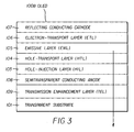
- a transmission enhancement layer (TEL) 109 is placed between the transparent substrate 101 and a semitransparent conducting reflecting anode 108 made of metal or metal alloy is provided to further enhance the emission through the substrate 101.
- the OLED 100B is otherwise similar to device OLED 100A.
- OLED 100C In OLED 100C (FIG. 4) a conducting reflector 111 is used regardless of the work function.
- the conducting reflector 111 is deposited on the ultrathin cathode 110, which is formed over the electron-transport layer 106.
- the OLED 100C is otherwise similar to OLED 100B.
- a conducting reflecting anode 108x is a fully reflective layer deposited over a transparent or opaque substrate 101x.
- composition and the function of the various layers constituting the OLED device are described as follows.
- Substrate 101 may include glass, ceramic, or plastics. For devices emitting through substrate 101, the substrates should be as transparent as possible. Since the OLED device fabrication does not require high temperature process, any substrate 101 that can withstand process temperatures of the order of 100 °C is useful, which includes most thermal plastics.
- the substrate 101 may take the form of rigid plate, flexible sheet, or curved surfaces.
- Substrate 101 may include support with electronic backplane, and thus includes active-matrix substrates, which contain electronic addressing and switching elements. Active-matrix substrates may contain high temperature polysilicon thin-film-transistors, low temperature polysilicon thin-film-transistors or amorphous silicon thin film transistors. Those skilled in the art will appreciate that other circuit elements can be used to address and drive the OLED devices.
- Anode 102 provides the function of injecting holes into the organic layer when a positive potential relative to the cathode 107 is applied to the OLED 100. It has been shown, for example, in commonly assigned US-A-4,720,432, that indium tin oxide (ITO) forms an efficient anode because it has a relatively high work function. Since the ITO film itself is transparent and conducting, commercially available ITO-coated glass provides an excellent support for the fabrication of OLED 100 type devices (FIG. 1). OLED 100A type devices (FIG. 2) use a conducting and semitransparent metal/alloy layer as the anode 108 which is deposited on the transparent substrate 101. The anode 108 can be deposited by conventional deposition processes and may also be compatible with the manufacturing process for OLED 100. This anode 108 may or may not need an overlying hole-injecting layer 103.
- ITO indium tin oxide
- Hole-injection layer 103 provides the function of increasing the efficiency of the hole-injection from the anode 102 (FIG. 1) or anode 108 of (FIG. 2) into the hole-transport layer. It has been shown, for example in commonly assigned US-A-4,885,211, that a porphorinic or phthalocyanine compound is useful as a hole injection layer 103 to the hole-transport layer 104 of the prior art type device (FIG. 1), resulting in increased luminance efficiency and operational stability.
- Other preferred hole-injection materials include CF x , which is a fluorinated polymer deposited by plasma-assisted vapor deposition, wherein x is less than or equal to 2 and greater than 0.
- CF x The method of preparation and the characteristics of CF x have been disclosed in commonly assigned US-A-6,208,077.
- Other materials can also be used as hole injectors. These include oxides of Mo, V or Ru.
- a layer of these materials each about 30 nm thick on 120 nm thick ITO have been found useful as a hole injector to TPD, an hole-transport layer ("Metal oxides as a hole-injecting layer for an organic electroluminescent device", S. Tokito, K. Noda and Y. Taga, J. Phys. D; Appl. Phys. 29, 2750 (1996)).
- CF x and MoO x (x ⁇ 3.0) were found to provide efficient hole injection from the metal anode 108 or anode 108x to the hole-transport layer 104 of FIG. 2, FIG. 3, or FIG. 4 or FIG. 5.
- MoO x layer is prepared by vacuum evaporation of MoO 3 and the deposited film may be non-stoichiometric.
- Other hole injectors for metal anodes may include ITO, IZO, Pr 2 O 3 , TeO 2 , CuPc, or SiO 2 .
- Hole-transport layer 104 provides the function of transporting holes to the emissive layer 105.
- Hole-transport materials include various classes of aromatic amines as disclosed in commonly assigned US-A-4,720,432.
- a preferred class of hole-transport materials includes the tetraaryldiamines of formula (I). wherein:
- Useful selected (fused aromatic ring containing) aromatic tertiary amines are the following:
- Emissive layer 105 provides the function of light emission produced as a result of recombination of holes and electrons in this layer.
- a preferred embodiment of the emissive layer 105 includes a host material doped with one or more fluorescent dyes. Using this host-dopant composition, highly efficient OLED devices can be constructed. Simultaneously, the color of the EL devices can be tuned by using fluorescent dyes of different emission wavelengths in a common host material. Tang and others in commonly assigned US-A-4,769,292 has described this dopant scheme in considerable detail for OLED devices using Alq as the host material.
- the emissive layer can contain a green light-emitting doped material, a blue light-emitting doped material, or a red light-emitting doped material.
- Preferred host materials include the class of 8-quinolinol metal chelate compounds with the chelating metals being Al, Mg, Li, Zn, for example.
- Another preferred class of host materials includes anthracene derivatives such as 9,10 dinaphthyl anthracene; 9,10 dianthryl anthracene; and alkyl substituted 9,10 dinaphthyl anthracene, as disclosed in Shi and others commonly assigned US-A-5,935,721.
- Dopant materials include most fluorescent and phorphorescent dyes and pigments.
- Preferred dopant materials include coumarins such as coumarin 6, dicyanomethylenepyrans such as 4-dicyanomethylene-4H pyrans, as disclosed in Tang and others commonly assigned US-A-4,769,292 and in Chen and others in commonly assigned US-A-6,020,078.
- Electron-transport layer 106 provides the function of delivering electrons injected from the cathode to emissive layer 105 (FIGS. 1-5).
- Useful materials include Alq, benzazoles, as disclosed in commonly assigned Shi and others commonly assigned US-A-5,645,948.
- Cathode 107 is typically a conducting and fully reflective thin film, about 50 to 500 nm thick, and comprised of materials including alloys capable of efficiently injecting electrons into the electron-transport layer 106 (FIGS. 1-3).
- Mg and Li containing alloys are generally used because they have low work functions and make efficient electron-injecting contacts to Alq electron-transport layer 106.
- Other materials with work-functions of ⁇ 4.0 eV can also be used as the electron injectors. These include metal or metal alloys including alloys of Ag or Al with Mg, alkali metals, alkali earth metals, or Mn.
- the cathode 107x is generally vapor deposited on electron-transport layer 106 (FIGS. 1-3).
- Cathode 107x (FIG. 5) is a semitransparent film about 4 to 50 nm thick also vapor deposited and includes a low work function ( ⁇ 4 eV) metal and metal alloys including alloys of Ag or Al with Mg, alkali metals, alkali earth metals, or Mn.
- a low work function ( ⁇ 4 eV) metal and metal alloys including alloys of Ag or Al with Mg, alkali metals, alkali earth metals, or Mn.
- Anode 108 is a reflective, weakly absorbing, and conductive film and comprised of materials including alloys having significant transmittance at the emission wavelength.
- Such metals include Ag, Al, Mg, Zn, Rh, Ru, Ir, Au, Cu, Pd, Ni, Cr, Pt, Co, Te, or Mo, or alloys or mixtures thereof.
- weakly absorbing it is meant that the absorption of a film on glass is less than 30%.
- the reflectivity of such layers can be about 30% or greater.
- the thickness of the layer should be greater than about 4 nm but less than about 50 nm.
- 5) is a conducting and fully reflecting layer, 50 to 500 nm thick and includes Ag, Al, Mg, Zn, Rh, Ru, Ir, Au, Cu, Pd, Ni, Cr, Pt, Co, Te, Mo, Hf, Fe, Mn, Nb, Ge, Os, Ti, V, or W, or alloys or mixtures thereof.
- Transmission enhancement layer 109 (FIGS. 3 and 4) is a highly transmissive film inserted between the substrate 101 and the semitransparent anode 108 to further increase the emission through substrate 101.
- the transmission enhancement layer 109x (FIG. 5) is also a highly transmissive film deposited over the reflecting conducting cathode 107x to further increase the emission through semitransparent reflecting conducting cathode 107x.
- the transmission enhancement layers 109 and 109x include conductive or nonconductive materials including but not limited to: ITO, indium zinc oxide (IZO), tin oxide (TO), antimony-doped tin oxide (ATO), fluorine-doped tin oxide (FTO), indium oxide (IO), zinc oxide (ZO), cadmium stannate (CTO), cadmium oxide, phosphorus-doped TO, and aluminum-doped ZO, MgO, MoO x , SiO 2 Al 2 O 3 TiO 2 , ZrO 2 , SiN, AIN, TiN, ZrN, SiC, or Al 4 C 3 , or mixtures thereof.
- the thickness of transmission enhancement layers 109 or 109x can range from 20 nm to 150 nm.
- An ultrathin cathode 110 (FIG. 4) is effectively a transparent electron injecting layer formed over the electron-transport layer 106.
- Such cathodes 110 are prepared by depositing an ultrathin layer of an alkali metal or alkali earth metal or combinations thereof.
- the cathode 110 can also be prepared by depositing a compound of the metals and an activator metal like Al, Mg and so forth.
- Such a cathode 110 allows the use of any metal/alloy regardless of the work-function as the top electrode.
- the reflector 111 (FIG. 4) is typically a reflective layer of high reflectivity metal that may include but is not limited to Au, Ag, Cu, Al, or alloys thereof.
- the reflector reflects the light that emits toward the cathode and redirects it toward the substrate.
- a high reflectivity reflector helps to remarkably enhance emission through substrate, other lower reflectivity metals such as Mg, Zn, Ni, Pd, or Pt or alloys or mixtures thereof may be useful.
- the thickness of the reflector is chosen large enough to provide maximum reflectivity.
- the organic materials mentioned above are suitably deposited by evaporation in high vacuum.
- the metal/alloy layers are also vapor deposited although it is possible to use sputtering deposition if the device architecture includes a buffer (P.K. Raychaudhuri and J.K. Madathil, "Fabrication of Sputtered Cathodes for Organic Light-Emitting Diodes Using Transparent Buffer", Proceedings of the 7th Asian Symposium on Information Display (Sept 2 -4, Singapore a) Digest, paper 50; Vol. 32, pp. 55-58, 2001).
- OLED devices are sensitive to moisture or oxygen or both, so they are commonly sealed in an inert atmosphere such as nitrogen or argon, along with a desiccant such as alumina, bauxite, calcium sulfate, clays, silica gel, zeolites, alkaline metal oxides, alkaline earth metal oxides, sulfates, or metal halides and perchlorates.
- a desiccant such as alumina, bauxite, calcium sulfate, clays, silica gel, zeolites, alkaline metal oxides, alkaline earth metal oxides, sulfates, or metal halides and perchlorates.
- Methods for encapsulation and desiccation include, but are not limited to, those described in US-A-6,226,890.
- barrier layers such as SiO x , Teflon, and alternating inorganic/polymeric layers are known in the art for encapsulation.
- OLED devices of this invention can employ various well-known optical effects in order to enhance their properties if desired. This includes optimizing layer thicknesses to yield maximum light transmission, replacing reflective electrodes with light-absorbing electrodes to enhance contrast, providing anti-glare or anti-reflection coatings over the display, providing a polarizing medium over the display, or providing colored, neutral density, or color conversion filters over the display. Filters, polarizers, and anti-glare or anti-reflection coatings may be specifically provided over the cover or as part of the cover.
- Prior art devices were fabricated using glass substrates having a commercial grade 42-nm thick, 70-ohm/sq patterned ITO layer. After routine cleaning, a layer of 1-nm thick CF x HIL was deposited on the ITO surface by decomposing CHF 3 gas in RF plasma.
- the substrates for the devices of the present invention were glass plates upon which was deposited a weakly absorbing metal layer by sputtering in Ar containing atmosphere. These metallized glass substrates were also coated either with the said CF x hole injection layer or with a vapor deposited MoO x hole injection layer.
- the substrates were then transferred to a vacuum coater operating at ⁇ 1 x 10 -6 Torr, where the organic stack consisting of HTL, EML, ETL were deposited in sequence.
- a cathode layer of MgAg or of LiF/ MgAg was then deposited through a square mask, which defined an active area of 0.1 cm 2 for the device.
- the devices were hermetically encapsulated in a glove box filled with dry nitrogen.
- the luminance of the devices was determined using a Photo Research PR650 spectroradiometer as a function of current.
- the drive voltage and luminance given here are those obtained when a current corresponding to 20 mA/cm 2 was passed through the devices and luminance being determined in the direction normal to the device surface.
- the voltage drop caused by series resistance of the ITO layer or the semitransparent anode layer 108 or 108x was subtracted from the measured drive voltage in order to compare devices on the basis of their "true" drive voltage.
- a prior art device was made using ITO as the transparent anode, CF x as the HIL, Alq as the EML/ETL and a LiF/MgAg layer as the cathode (top electrode).
- the top electrode comprising 90% Mg and 10 % Ag by volume (hereafter MgAg) is 100 nm thick, fully reflective and opaque.
- the device is optimized for maximization of bottom emission.
- the device has the following layer structure:
- the light emerges through substrate.
- the drive voltage was 7.8 V and the emission was 641 cd/m 2 .
- the efficiency of the device is 3.2 cd/A.
- the peak emission wavelength is 525 nm.
- a device according to the present invention was made using a semitransparent Ag anode, MoO x as the HIL, Alq as the EML/ETL, and a LiF/MgAg layer as the cathode (top electrode).
- the MgAg layer is fully reflective and opaque.
- the device is optimized for maximization of bottom emission.
- the device has the following layer structure:
- the light emerges through substrate.
- the drive voltage was 6.9 V and the bottom emission was 1346 cd/m 2 .
- the efficiency of the device is 6.7 cd/A.
- the peak emission wavelength is 525 nm.
- Examples 1 and 2 show that the device of the present invention is more than twice as efficient as the prior art device and that the emission wavelength remains unchanged.
- a prior art device (3F) having a 42 nm thick ITO anode, and a series of devices of present invention (devices 3A, 3B, 3C, 3D and 3E) each having a semitransparent Ag anode layer were made.
- the device structure in each case was optimized for maximization of bottom emission by selecting the NPB layer thickness.
- the hole-injection layer for each of the devices was a 1 nm thick CF x layer. All devices also used 30 nm thick Alq doped with 1% C545T as the emitter, 30 nm thick undoped Alq as the electron-transport layer, and 100 nm thick MgAg layer as the cathode. The results are tabulated in Table 2.
- Example 3 show that devices of the present invention having a semitransparent Ag anode in the thickness range between 10 nm and 30 nm (devices 3E, 3D and 3C) exhibit luminance that is greater than that of the prior art device (3F).
- the efficiency of the device having the 20nm Ag anode is about 2 times the efficiency of the prior art device (3F).
- a prior art device (4F) having a 42 nm thick ITO anode, and a series of devices of present invention (devices 4A, 4B, 4C, 4D and 4E) each having a semitransparent Au anode layer were made.
- the device structure in each case was optimized for maximization of bottom emission by selecting the NPB layer thickness.
- the hole-injection layer for each of the devices was a 1 nm thick CF x layer. All devices also used 30 nm thick Alq doped with 1% DCJTB as the emitter, 30 nm thick undoped Alq as the electron-transport layer, and 100 nm thick MgAg layer as the cathode.
- Table 3 The results are tabulated in Table 3.
- Example 4 show that devices of the present invention having a semitransparent Au anode in the thickness range between 15 nm and 40 nm (devices 4E, 4D, 4C and 4B) exhibit emission that is greater than that of the prior art device (4F).
- the efficiency of the device (4D) having the 20nm Au anode is about 2 times the efficiency of the prior art device (4F).
- Optical modeling was performed on a prior art device structure: device 5A -- Glass (1.1 mm)/ ITO(42nm)/ NPB(105 nm)/Alq(60nm)/ MgAg(100 nm) and a device of the present invention: device 5B-- Glass (1.1 mm)/ Mo(5 nm)/ NPB(50 nm)/Alq (60nm)/ MgAg(100 nm).
- the presence in the stack of ultrathin layer of CF x or MoO x have been neglected.
- the output of the device 5B was found to be about 92% when compared with that of the device 5A.
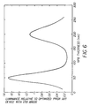
- Optical modeling was performed on a prior art device structure: device 6A -- Glass(1.1 mm)/ ITO(42nm)/ NPB(105 nm)/Alq(60nm)/ MgAg(100 nm) and a series of devices of the present invention having varying thickness of the HTL layer: Glass(1.1 mm)/Ag(20 nm)/NPB(vary)/Alq (60nm)/MgAg(100 nm).
- the presence in the stack of ultrathin layer of CF x or MoO x have been neglected. The results show that on-axis maximum luminance occurs at 50 nm (1 st maximum) and at 200 nm (2 nd maximum), as shown in FIG. 6.
- the luminance of the device of the present invention is about 1.7 times that of the optimized bottom-emitting prior art device 6A. This is in fair agreement with the experimental data presented in the above examples.
- the OLED of the present invention in the thickness range 20 nm to 80 nm or 180 nm to 230 nm of NPB is predicted to exceed the luminance of the prior art device.
- the total thickness of the organic layers between electrodes for high efficiency bottom emitters are either 80 nm to 140 nm or 240 nm to 290 nm for the first or second maximum, respectively.
- a series of top emitters of the present invention each having a 60 nm thick Ag anode, a semitransparent cathode, and varying NPB layer thickness was made.
- the HIL for each of the devices was a 1 nm thick CF x .
- For all devices used were 30 nm thick Alq doped with 1% C545T as the EML, 30 nm thick undoped Alq as the ETL, and 14 nm thick semitransparent MgAg layer as the cathode.
- the devices do not have a TEL but are otherwise similar to the device of FIG. 5. The results are tabulated in Table 4.
- Example 7 show that for devices of the present invention having a semitransparent MgAg cathode, the luminance is maximized when the thickness of the NPB layer is 50 nm.
- a simulation similar to Example 6 predicts that the first maximum in on-axis luminance occurs at the NPB thickness of 45nm and that the second maximum occurs at the NPB thickness of 180 nm.
- the ideal thickness of the organic medium for maximization of top-emission is thus either 105 nm or 240 nm.
- Devices with high efficiency can be made in the NPB thickness range between 30 nm to 80 nm or 160 nm to 230 nm. This leads to total organic layer thickness 90 nm to 140nm or 220 nm to 290 nm.
- top-emitters of the present invention were made using various reflective anodes but all having a common 14 nm MgAg cathode, and common organic layers-50 nm NPB hole-transport layer and 60 nm Alq EML/ETL.
- the reflectors used were fully reflective films of Ag, Pd and Mo.
- the reflectivities of fully reflective film in air at ⁇ 525 nm, taken from the literature, are also tabulated in Table 5.
- the hole-injection layer for each of the devices was a MoO x film, 1 nm thick. The device does not have a TEL.
- the device performance is tabulated in Table 5.
- Example 8 show that the top emission is an increasing function of anode reflectivity. But the output is not simply proportional to anode reflectivity; rather, it rises significantly more rapidly in the high reflectivity range. If the advantage of top-emitter over bottom-emitter with respect to aperture ratio is considered then even the top emitter having a Mo anode is expected to outperform a bottom emitter having an ITO anode.
- Two top-emitting devices of the present invention were made each having a 72 nm thick Ag anode, 2.5 nm thick MoO x HIL, 45 nm thick NPB HTL and 60 nm Alq EML/ETL and 0.5 nm LiF/ 14 nm MgAg cathode.
- the device 9A does not have a TEL.
- On the cathode of the device 9B was deposited a 85 nm Alq layer as the TEL.
- the device 9A At a drive current corresponding to 20 mA/cm 2 the device 9A has a drive voltage of 7.3 V and a luminance of 1260 cd/m 2 .
- the device 9B Under similar condition the device 9B has a drive voltage of 7.1 V and a luminance of 1630 cd/m 2.
- the 85 nm Alq layer has acted as a TEL.
- the improvement due to the TEL is about 29%.
- the on-axis emission through the substrate can be greater than that of a prior art control device that has a low-reflectivity, highly-transparent ITO anode.
- the device architecture has to be altered.
- the emission from a microcavity is strongly directed along the optical axis (normal to the emitting plane).
- the loss of light in OLED devices 100A, 100B or 100C (FIGS. 2-4) due to absorption in the anode can be more than compensated by the gain due to the microcavity effect.
- An optical microcavity OLED somewhat similar to that of the present invention is reported in the literature ("Control of emission characteristics in organic thin-film electro luminescent devices using an optical-microcavity structure" N. Takada, T. Tsutsui, and S. Saito, Appl. Phys. Lett. 63, 2032 (1993)).
- a microcavity structure which comprised a reflective, semitransparent, 36 nm thick Ag anode and a reflective 250 nm thick MgAg cathode was fabricated.
- a device without the microcavity structure with a transparent ITO anode was also prepared for reference. These two devices were made on one support and had common organic layers and cathode.
- the microcavity device did not exhibit enhancement of bottom emission over that of the non-microcavity device.
- the microcavity device characteristically exhibited angular dependence of emission and emission peak shift with viewing angle.
- the emission from the microcavity device was weaker than that of the non-microcavity device.
- the thick anode, the non-optimized device structure, and, more importantly, the absence of a hole-injecting layer may have resulted in an inefficient device. Optimization of these three aspects is the most distinguishing feature that is incorporated in the present invention.
- the bottom-emitting OLED device wherein the plurality of organic layers includes a hole-transport layer disposed between the hole injection layer and the emissive layer.
- the bottom-emitting OLED device wherein the reflective, weakly absorbing, and conductive anode includes Ag, Al, Mg, Zn, Rh, Ru, Ir, Au, Cu, Pd, Ni, Cr, Pt, Co, Te, or Mo or alloys or mixtures thereof.
- the bottom-emitting OLED device wherein the reflective, weakly absorbing, and conductive anode layer has an absorbance of 30% or less.
- the bottom-emitting OLED device wherein the reflective and conductive cathode includes metal or metal alloys having a work function selected to be about 4.0 eV or less.
- the bottom-emitting OLED device wherein the metal or metal alloys include alloys of Ag or Al with Mg, alkali metals, alkali earth metals, or Mn.
- the bottom-emitting OLED device wherein the hole injection layer includes CF x , ITO, IZO, Pr 2 O 3 , TeO 2 , CuPc, SiO 2 , VO x , MoO x , or mixtures thereof.
- the bottom-emitting OLED device wherein the emissive layer contains fluorescent or phosphorescent dopants.
- the bottom-emitting OLED device wherein the thickness of the hole-transport layer is in the range of 20 nm to 80 nm or 180 nm to 230 nm.
- the bottom-emitting OLED device wherein the thickness of the anode layer is in a range of from 4 nm to 50 nm.
- the bottom-emitting OLED device wherein the thickness of the cathode layer is in a range of from 50 nm to 500 nm.
- the bottom-emitting OLED device which includes an ultrathin cathode over the electron transport layer.
- the bottom-emitting OLED device which further includes a highly reflective, substantially opaque metal/alloy over the ultrathin cathode.
- the bottom-emitting OLED device wherein the highly reflective, substantially opaque metals include Ag, Al, Mg, Zn, Au or Cu or alloys or mixtures thereof.
- the top-emitting OLED device wherein the plurality of organic layers includes a hole-transport layer disposed between the hole injection layer and the emissive layer.
- the top-emitting OLED device wherein the reflective, substantially opaque and conductive anode includes Ag, Al, Mg, Zn, Rh, Ru, Ir, Au, Cu, Pd, Ni, Cr, Pt, Co, Te, Mo, Hf, Fe, Mn, Nb, Ge, Os, Ti, V or W, or alloys or mixtures thereof.
- the top-emitting OLED device wherein the reflective, semitransparent and conductive cathode has an absorbance of 30% or less.
- the top-emitting OLED device wherein the thickness of the TEL ranges from 20 nm to 150 nm.
- the top-emitting OLED device wherein the emissive layer contains fluorescent or phosphorescent dopants.
- the top-emitting OLED device wherein the thickness of the hole-transport layer is 30 to 80 nm or 160 to 230 nm.
- the top-emitting OLED device wherein the total thickness of organic layers is 90 to 140 nm or 220 to 290 nm.
- the top-emitting OLED device wherein the thickness of the anode layer is in a range of from 50 nm to 500 nm
- the top-emitting OLED device wherein the thickness of the cathode layer is in a range of from 5 nm to 50 nm.
- the top-emitting OLED device which includes an ultrathin cathode over the electron transport layer.
- the top-emitting OLED device which further includes a highly reflective, semitransparent metal/alloy over the ultrathin cathode.
- the top-emitting OLED device wherein the highly reflective, semitransparent metals include Ag, Al, Mg, Zn, Au or Cu or alloys or mixtures thereof.
Landscapes
- Physics & Mathematics (AREA)
- Optics & Photonics (AREA)
- Engineering & Computer Science (AREA)
- Mechanical Engineering (AREA)
- Electroluminescent Light Sources (AREA)
Applications Claiming Priority (2)
| Application Number | Priority Date | Filing Date | Title |
|---|---|---|---|
| US347013 | 1994-11-30 | ||
| US10/347,013 US20040140758A1 (en) | 2003-01-17 | 2003-01-17 | Organic light emitting device (OLED) display with improved light emission using a metallic anode |
Publications (1)
| Publication Number | Publication Date |
|---|---|
| EP1439588A2 true EP1439588A2 (de) | 2004-07-21 |
Family
ID=32594895
Family Applications (1)
| Application Number | Title | Priority Date | Filing Date |
|---|---|---|---|
| EP03079143A Withdrawn EP1439588A2 (de) | 2003-01-17 | 2003-12-19 | Organische lichtemittierende Dioden- (OLED) Anzeige mit metallischer Anode zur verbesserten Lichtemission |
Country Status (5)
| Country | Link |
|---|---|
| US (1) | US20040140758A1 (de) |
| EP (1) | EP1439588A2 (de) |
| JP (1) | JP2004228081A (de) |
| KR (1) | KR20040066724A (de) |
| TW (1) | TW200423798A (de) |
Cited By (7)
| Publication number | Priority date | Publication date | Assignee | Title |
|---|---|---|---|---|
| US7505487B2 (en) | 2003-04-23 | 2009-03-17 | Semiconductor Energy Laboratory Co., Ltd. | Laser oscillator including phosphorescent material |
| CN102473860A (zh) * | 2009-07-27 | 2012-05-23 | 欧司朗光电半导体有限公司 | 电子器件以及电接触部 |
| US8207555B2 (en) | 2004-11-05 | 2012-06-26 | Semiconductor Energy Laboratory Co., Ltd. | Light-emitting element and light emitting device using the same |
| CN102610763A (zh) * | 2010-12-22 | 2012-07-25 | 日东电工株式会社 | 有机el元件的制造方法和制造装置 |
| CN102891265A (zh) * | 2012-09-28 | 2013-01-23 | 昆山工研院新型平板显示技术中心有限公司 | Oled阳极的增反结构和oled阴极的增反结构 |
| CN103035854A (zh) * | 2012-11-30 | 2013-04-10 | 江苏威纳德照明科技有限公司 | 一种包括电子传输层的高分子发光二极管的制造方法 |
| CN114497416A (zh) * | 2022-01-25 | 2022-05-13 | 南方科技大学 | 显示器件及其制备方法 |
Families Citing this family (109)
| Publication number | Priority date | Publication date | Assignee | Title |
|---|---|---|---|---|
| KR100563675B1 (ko) * | 2002-04-09 | 2006-03-28 | 캐논 가부시끼가이샤 | 유기 발광소자 및 유기 발광소자 패키지 |
| US20040155576A1 (en) * | 2003-01-17 | 2004-08-12 | Eastman Kodak Company | Microcavity OLED device |
| US6861800B2 (en) * | 2003-02-18 | 2005-03-01 | Eastman Kodak Company | Tuned microcavity color OLED display |
| TW595259B (en) * | 2003-01-28 | 2004-06-21 | Ind Tech Res Inst | Organic electroluminescent device |
| KR100528916B1 (ko) * | 2003-06-25 | 2005-11-15 | 삼성에스디아이 주식회사 | 배면발광형 전계발광소자 |
| TWI407830B (zh) | 2003-09-26 | 2013-09-01 | 半導體能源研究所股份有限公司 | 發光元件和其製法 |
| KR20060110323A (ko) | 2003-12-16 | 2006-10-24 | 마츠시타 덴끼 산교 가부시키가이샤 | 유기 전기발광 소자 및 그 제조 방법 |
| WO2005064995A1 (en) * | 2003-12-26 | 2005-07-14 | Semiconductor Energy Laboratory Co., Ltd. | Light-emitting element |
| US7049741B2 (en) * | 2004-01-27 | 2006-05-23 | Eastman Kodak Company | Organic light emitting diode with improved light emission through substrate |
| WO2006008987A1 (ja) * | 2004-07-15 | 2006-01-26 | Idemitsu Kosan Co., Ltd. | 有機el表示装置 |
| JP4086817B2 (ja) * | 2004-07-20 | 2008-05-14 | キヤノン株式会社 | 有機el素子 |
| JP2006295104A (ja) * | 2004-07-23 | 2006-10-26 | Semiconductor Energy Lab Co Ltd | 発光素子およびそれを用いた発光装置 |
| WO2006022193A1 (en) * | 2004-08-23 | 2006-03-02 | Semiconductor Energy Laboratory Co., Ltd. | Light emitting element, light emitting device, and lighting system |
| JP2006092936A (ja) * | 2004-09-24 | 2006-04-06 | Toyota Industries Corp | 有機el装置 |
| CN101841002B (zh) * | 2004-09-24 | 2011-11-16 | 株式会社半导体能源研究所 | 发光器件 |
| US20070262693A1 (en) | 2004-10-29 | 2007-11-15 | Satoshi Seo | Composite Material, Light-Emitting Element, Light-Emitting Device and Manufacturing Method Thereof |
| JP2006154169A (ja) * | 2004-11-29 | 2006-06-15 | Seiko Epson Corp | 電気光学素子の製造方法、電気光学装置 |
| US8569948B2 (en) * | 2004-12-28 | 2013-10-29 | Samsung Display Co., Ltd. | Electroluminescent devices and methods of making electroluminescent devices including an optical spacer |
| TWI245587B (en) * | 2005-02-17 | 2005-12-11 | Au Optronics Corp | Organic electro luminescence devices, flat panel displays, and portable electronics using the same |
| KR100721571B1 (ko) * | 2005-03-07 | 2007-05-23 | 삼성에스디아이 주식회사 | 유기 전계 발광 소자 및 그의 제조방법 |
| CN100524890C (zh) * | 2005-03-21 | 2009-08-05 | 友达光电股份有限公司 | 有机电激发光元件、平面显示器及可携带式电子装置 |
| US8420227B2 (en) | 2005-03-23 | 2013-04-16 | Semiconductor Energy Laboratory Co., Ltd. | Composite material, light emitting element and light emitting device |
| US7851989B2 (en) * | 2005-03-25 | 2010-12-14 | Semiconductor Energy Laboratory Co., Ltd. | Light emitting device |
| WO2006108272A2 (en) * | 2005-04-12 | 2006-10-19 | Zheng-Hong Lu | Metal/fullerene anode structure and application of same |
| US8334057B2 (en) | 2005-06-08 | 2012-12-18 | Semiconductor Energy Laboratory Co., Ltd. | Light-emitting element, light-emitting device, and electronic device |
| US20070096086A1 (en) * | 2005-06-27 | 2007-05-03 | Ying Wang | Hole injection electrode |
| US8415878B2 (en) | 2005-07-06 | 2013-04-09 | Semiconductor Energy Laboratory Co., Ltd. | Light-emitting element, light-emitting device, and electronic device |
| US7994711B2 (en) * | 2005-08-08 | 2011-08-09 | Semiconductor Energy Laboratory Co., Ltd. | Light emitting device and manufacturing method thereof |
| KR20070019495A (ko) * | 2005-08-12 | 2007-02-15 | 삼성에스디아이 주식회사 | 백색 유기 발광 소자 및 그의 제조방법 |
| TW200721478A (en) * | 2005-10-14 | 2007-06-01 | Pioneer Corp | Light-emitting element and display apparatus using the same |
| KR20070069314A (ko) * | 2005-12-28 | 2007-07-03 | 전자부품연구원 | Oled 소자 |
| KR20070097139A (ko) * | 2006-03-23 | 2007-10-04 | 엘지전자 주식회사 | 적색 인광 화합물 및 이를 사용한 유기전계발광소자 |
| US7622865B2 (en) * | 2006-06-19 | 2009-11-24 | Seiko Epson Corporation | Light-emitting device, image forming apparatus, display device, and electronic apparatus |
| JP5109303B2 (ja) | 2006-07-31 | 2012-12-26 | ソニー株式会社 | 有機発光素子および表示装置 |
| JP2008112904A (ja) * | 2006-10-31 | 2008-05-15 | Idemitsu Kosan Co Ltd | 有機エレクトロルミネッセンス素子 |
| TWI323826B (en) * | 2006-11-15 | 2010-04-21 | Ether Precision Inc | The manufacturing process of the combine of optical lens and chip |
| CN101271869B (zh) * | 2007-03-22 | 2015-11-25 | 株式会社半导体能源研究所 | 发光器件的制造方法 |
| JP5007170B2 (ja) * | 2007-07-20 | 2012-08-22 | 株式会社ジャパンディスプレイイースト | 有機el表示装置 |
| JP2010080950A (ja) * | 2008-08-29 | 2010-04-08 | Semiconductor Energy Lab Co Ltd | 固体色素レーザ |
| US8494021B2 (en) * | 2008-08-29 | 2013-07-23 | Semiconductor Energy Laboratory Co., Ltd. | Organic laser device |
| JP5138542B2 (ja) * | 2008-10-24 | 2013-02-06 | パナソニック株式会社 | 有機エレクトロルミネッセンス素子及びその製造方法 |
| US8643000B2 (en) * | 2008-11-18 | 2014-02-04 | E I Du Pont De Nemours And Company | Organic electronic device with low-reflectance electrode |
| JP2010153365A (ja) * | 2008-11-19 | 2010-07-08 | Semiconductor Energy Lab Co Ltd | 発光素子、発光装置、電子機器及び照明装置 |
| US9948872B2 (en) | 2009-03-02 | 2018-04-17 | Flir Systems, Inc. | Monitor and control systems and methods for occupant safety and energy efficiency of structures |
| US9998697B2 (en) | 2009-03-02 | 2018-06-12 | Flir Systems, Inc. | Systems and methods for monitoring vehicle occupants |
| US9843742B2 (en) | 2009-03-02 | 2017-12-12 | Flir Systems, Inc. | Thermal image frame capture using de-aligned sensor array |
| US9208542B2 (en) | 2009-03-02 | 2015-12-08 | Flir Systems, Inc. | Pixel-wise noise reduction in thermal images |
| US9635285B2 (en) | 2009-03-02 | 2017-04-25 | Flir Systems, Inc. | Infrared imaging enhancement with fusion |
| US9517679B2 (en) | 2009-03-02 | 2016-12-13 | Flir Systems, Inc. | Systems and methods for monitoring vehicle occupants |
| USD765081S1 (en) | 2012-05-25 | 2016-08-30 | Flir Systems, Inc. | Mobile communications device attachment with camera |
| US9235876B2 (en) | 2009-03-02 | 2016-01-12 | Flir Systems, Inc. | Row and column noise reduction in thermal images |
| US9756264B2 (en) | 2009-03-02 | 2017-09-05 | Flir Systems, Inc. | Anomalous pixel detection |
| US9674458B2 (en) | 2009-06-03 | 2017-06-06 | Flir Systems, Inc. | Smart surveillance camera systems and methods |
| US9986175B2 (en) | 2009-03-02 | 2018-05-29 | Flir Systems, Inc. | Device attachment with infrared imaging sensor |
| US9451183B2 (en) | 2009-03-02 | 2016-09-20 | Flir Systems, Inc. | Time spaced infrared image enhancement |
| US10757308B2 (en) | 2009-03-02 | 2020-08-25 | Flir Systems, Inc. | Techniques for device attachment with dual band imaging sensor |
| US9473681B2 (en) | 2011-06-10 | 2016-10-18 | Flir Systems, Inc. | Infrared camera system housing with metalized surface |
| US10244190B2 (en) | 2009-03-02 | 2019-03-26 | Flir Systems, Inc. | Compact multi-spectrum imaging with fusion |
| US10091439B2 (en) | 2009-06-03 | 2018-10-02 | Flir Systems, Inc. | Imager with array of multiple infrared imaging modules |
| US9756262B2 (en) | 2009-06-03 | 2017-09-05 | Flir Systems, Inc. | Systems and methods for monitoring power systems |
| US9716843B2 (en) | 2009-06-03 | 2017-07-25 | Flir Systems, Inc. | Measurement device for electrical installations and related methods |
| US9819880B2 (en) | 2009-06-03 | 2017-11-14 | Flir Systems, Inc. | Systems and methods of suppressing sky regions in images |
| US9843743B2 (en) | 2009-06-03 | 2017-12-12 | Flir Systems, Inc. | Infant monitoring systems and methods using thermal imaging |
| US9292909B2 (en) | 2009-06-03 | 2016-03-22 | Flir Systems, Inc. | Selective image correction for infrared imaging devices |
| US8137148B2 (en) * | 2009-09-30 | 2012-03-20 | General Electric Company | Method of manufacturing monolithic parallel interconnect structure |
| KR20110038513A (ko) * | 2009-10-08 | 2011-04-14 | 삼성모바일디스플레이주식회사 | 유기 발광 표시 장치 및 그 제조 방법 |
| US8404500B2 (en) | 2009-11-02 | 2013-03-26 | Semiconductor Energy Laboratory Co., Ltd. | Method for manufacturing light-emitting element, light-emitting element, light-emitting device, lighting device, and electronic appliance |
| US9848134B2 (en) | 2010-04-23 | 2017-12-19 | Flir Systems, Inc. | Infrared imager with integrated metal layers |
| US9918023B2 (en) | 2010-04-23 | 2018-03-13 | Flir Systems, Inc. | Segmented focal plane array architecture |
| US9706138B2 (en) | 2010-04-23 | 2017-07-11 | Flir Systems, Inc. | Hybrid infrared sensor array having heterogeneous infrared sensors |
| US9207708B2 (en) | 2010-04-23 | 2015-12-08 | Flir Systems, Inc. | Abnormal clock rate detection in imaging sensor arrays |
| US8742657B2 (en) * | 2010-06-11 | 2014-06-03 | Universal Display Corporation | Triplet-Triplet annihilation up conversion (TTA-UC) for display and lighting applications |
| JP5969216B2 (ja) | 2011-02-11 | 2016-08-17 | 株式会社半導体エネルギー研究所 | 発光素子、表示装置、照明装置、及びこれらの作製方法 |
| US9706137B2 (en) | 2011-06-10 | 2017-07-11 | Flir Systems, Inc. | Electrical cabinet infrared monitor |
| US9961277B2 (en) | 2011-06-10 | 2018-05-01 | Flir Systems, Inc. | Infrared focal plane array heat spreaders |
| US9143703B2 (en) | 2011-06-10 | 2015-09-22 | Flir Systems, Inc. | Infrared camera calibration techniques |
| US9509924B2 (en) | 2011-06-10 | 2016-11-29 | Flir Systems, Inc. | Wearable apparatus with integrated infrared imaging module |
| US10841508B2 (en) | 2011-06-10 | 2020-11-17 | Flir Systems, Inc. | Electrical cabinet infrared monitor systems and methods |
| US10169666B2 (en) | 2011-06-10 | 2019-01-01 | Flir Systems, Inc. | Image-assisted remote control vehicle systems and methods |
| US10051210B2 (en) | 2011-06-10 | 2018-08-14 | Flir Systems, Inc. | Infrared detector array with selectable pixel binning systems and methods |
| EP2719167B1 (de) | 2011-06-10 | 2018-08-08 | Flir Systems, Inc. | Infrarotabbildung mit geringem stromverbrauch und geringem formfaktor |
| US9058653B1 (en) | 2011-06-10 | 2015-06-16 | Flir Systems, Inc. | Alignment of visible light sources based on thermal images |
| US10079982B2 (en) | 2011-06-10 | 2018-09-18 | Flir Systems, Inc. | Determination of an absolute radiometric value using blocked infrared sensors |
| US9235023B2 (en) | 2011-06-10 | 2016-01-12 | Flir Systems, Inc. | Variable lens sleeve spacer |
| US9900526B2 (en) | 2011-06-10 | 2018-02-20 | Flir Systems, Inc. | Techniques to compensate for calibration drifts in infrared imaging devices |
| US10389953B2 (en) | 2011-06-10 | 2019-08-20 | Flir Systems, Inc. | Infrared imaging device having a shutter |
| EP2719165B1 (de) | 2011-06-10 | 2018-05-02 | Flir Systems, Inc. | Ungleichmässigkeitskorrekturverfahren für infrarot-bildgebungsvorrichtungen |
| CN103828343B (zh) | 2011-06-10 | 2017-07-11 | 菲力尔系统公司 | 基于行的图像处理和柔性存储系统 |
| CN103311448A (zh) * | 2012-03-06 | 2013-09-18 | 海洋王照明科技股份有限公司 | 一种有机电致发光器件及其制备方法 |
| CN104620282B (zh) | 2012-07-16 | 2018-01-12 | 菲力尔系统公司 | 用于抑制图像中的噪声的方法和系统 |
| US9811884B2 (en) | 2012-07-16 | 2017-11-07 | Flir Systems, Inc. | Methods and systems for suppressing atmospheric turbulence in images |
| JP6419781B2 (ja) * | 2013-04-22 | 2018-11-07 | サノフィ−アベンティス・ドイチュラント・ゲゼルシャフト・ミット・ベシュレンクテル・ハフツング | Oledを備えたセンサデバイス |
| US9177513B2 (en) | 2013-05-22 | 2015-11-03 | Vizio, Inc | Electroluminescent display where each pixel can emit light of any EIA color index |
| US9973692B2 (en) | 2013-10-03 | 2018-05-15 | Flir Systems, Inc. | Situational awareness by compressed display of panoramic views |
| KR102207563B1 (ko) * | 2013-10-29 | 2021-01-27 | 삼성디스플레이 주식회사 | 유기 발광 표시장치 및 유기 발광 표시장치의 제조 방법 |
| KR102050243B1 (ko) * | 2013-12-02 | 2019-11-29 | 한국전자통신연구원 | 자발광형 소자 및 반사형 소자를 포함하는 이중모드 화소 및 이를 이용한 이중모드 디스플레이 |
| JP6475251B2 (ja) * | 2013-12-31 | 2019-02-27 | 昆山工研院新型平板顕示技術中心有限公司Kunshan New Flat Panel Display Technology Center Co., Ltd. | 有機発光表示装置及び視野角特性を改善したトップエミッション型oled装置 |
| US11297264B2 (en) | 2014-01-05 | 2022-04-05 | Teledyne Fur, Llc | Device attachment with dual band imaging sensor |
| US9640781B2 (en) | 2014-05-22 | 2017-05-02 | Universal Display Corporation | Devices to increase OLED output coupling efficiency with a high refractive index substrate |
| US9496523B1 (en) | 2015-06-19 | 2016-11-15 | Universal Display Corporation | Devices and methods to improve light outcoupling from an OLED array |
| KR102529684B1 (ko) * | 2015-11-30 | 2023-05-04 | 엘지디스플레이 주식회사 | 유기 발광 표시 장치 |
| EP3182478B1 (de) * | 2015-12-18 | 2018-11-28 | Novaled GmbH | Elektroneninjektionsschicht für eine organische leuchtdiode (oled) |
| KR102522667B1 (ko) * | 2016-06-13 | 2023-04-17 | 삼성디스플레이 주식회사 | 표시 장치 |
| TWI625740B (zh) * | 2016-12-28 | 2018-06-01 | 國立清華大學 | 透明導電結構及具有該透明導電結構的光電元件 |
| KR102802109B1 (ko) * | 2018-12-13 | 2025-04-28 | 엘지디스플레이 주식회사 | 부분 투명 표시장치 |
| KR20220033650A (ko) * | 2020-09-09 | 2022-03-17 | 삼성디스플레이 주식회사 | 반사 전극 및 이를 포함하는 표시 장치 |
| CN112310308B (zh) * | 2020-10-22 | 2022-04-26 | 深圳市华星光电半导体显示技术有限公司 | 显示面板及其制备方法 |
| KR20220162927A (ko) | 2021-06-01 | 2022-12-09 | 삼성디스플레이 주식회사 | 표시 장치 |
| WO2024016165A1 (zh) * | 2022-07-19 | 2024-01-25 | 京东方科技集团股份有限公司 | 显示面板及显示装置 |
Family Cites Families (15)
| Publication number | Priority date | Publication date | Assignee | Title |
|---|---|---|---|---|
| US4885211A (en) * | 1987-02-11 | 1989-12-05 | Eastman Kodak Company | Electroluminescent device with improved cathode |
| US4769292A (en) * | 1987-03-02 | 1988-09-06 | Eastman Kodak Company | Electroluminescent device with modified thin film luminescent zone |
| US5150006A (en) * | 1991-08-01 | 1992-09-22 | Eastman Kodak Company | Blue emitting internal junction organic electroluminescent device (II) |
| US5226053A (en) * | 1991-12-27 | 1993-07-06 | At&T Bell Laboratories | Light emitting diode |
| CN1152607C (zh) * | 1995-01-19 | 2004-06-02 | 出光兴产株式会社 | 有机电致发光装置,有机薄膜和三胺化合物 |
| WO1996025020A1 (en) * | 1995-02-06 | 1996-08-15 | Idemitsu Kosan Co., Ltd. | Multi-color light emission apparatus and method for production thereof |
| EP1342769B1 (de) * | 1996-08-19 | 2010-01-27 | TDK Corporation | Organische elektrolumineszente Vorrichtung |
| EP0966050A3 (de) * | 1998-06-18 | 2004-11-17 | Osram Opto Semiconductors GmbH & Co. OHG | Organische Leuchtdiode |
| US6048573A (en) * | 1998-11-13 | 2000-04-11 | Eastman Kodak Company | Method of making an organic light-emitting device |
| US6366017B1 (en) * | 1999-07-14 | 2002-04-02 | Agilent Technologies, Inc/ | Organic light emitting diodes with distributed bragg reflector |
| US6849869B1 (en) * | 1999-07-19 | 2005-02-01 | Dupont Displays, Inc. | Long lifetime polymer light-emitting devices with improved luminous efficiency and improved radiance |
| JP2001267074A (ja) * | 2000-03-22 | 2001-09-28 | Fuji Photo Film Co Ltd | 有機発光素子 |
| US6515314B1 (en) * | 2000-11-16 | 2003-02-04 | General Electric Company | Light-emitting device with organic layer doped with photoluminescent material |
| US6703780B2 (en) * | 2001-01-16 | 2004-03-09 | General Electric Company | Organic electroluminescent device with a ceramic output coupler and method of making the same |
| US6687266B1 (en) * | 2002-11-08 | 2004-02-03 | Universal Display Corporation | Organic light emitting materials and devices |
-
2003
- 2003-01-17 US US10/347,013 patent/US20040140758A1/en not_active Abandoned
- 2003-11-24 TW TW092132919A patent/TW200423798A/zh unknown
- 2003-12-19 EP EP03079143A patent/EP1439588A2/de not_active Withdrawn
-
2004
- 2004-01-16 KR KR1020040003364A patent/KR20040066724A/ko not_active Withdrawn
- 2004-01-16 JP JP2004009436A patent/JP2004228081A/ja active Pending
Cited By (11)
| Publication number | Priority date | Publication date | Assignee | Title |
|---|---|---|---|---|
| US7505487B2 (en) | 2003-04-23 | 2009-03-17 | Semiconductor Energy Laboratory Co., Ltd. | Laser oscillator including phosphorescent material |
| US8207555B2 (en) | 2004-11-05 | 2012-06-26 | Semiconductor Energy Laboratory Co., Ltd. | Light-emitting element and light emitting device using the same |
| US8338196B2 (en) | 2004-11-05 | 2012-12-25 | Semiconductor Energy Laboratory Co., Ltd. | Light-emitting element and light emitting device using the same |
| CN102473860A (zh) * | 2009-07-27 | 2012-05-23 | 欧司朗光电半导体有限公司 | 电子器件以及电接触部 |
| US9059423B2 (en) | 2009-07-27 | 2015-06-16 | Osram Opto Semiconductors Gmbh | Electronic component and electrical contact |
| CN102610763A (zh) * | 2010-12-22 | 2012-07-25 | 日东电工株式会社 | 有机el元件的制造方法和制造装置 |
| CN102610763B (zh) * | 2010-12-22 | 2015-12-16 | 日东电工株式会社 | 有机el元件的制造方法和制造装置 |
| CN102891265A (zh) * | 2012-09-28 | 2013-01-23 | 昆山工研院新型平板显示技术中心有限公司 | Oled阳极的增反结构和oled阴极的增反结构 |
| CN102891265B (zh) * | 2012-09-28 | 2015-10-07 | 昆山工研院新型平板显示技术中心有限公司 | Oled阳极的增反结构和oled阴极的增反结构 |
| CN103035854A (zh) * | 2012-11-30 | 2013-04-10 | 江苏威纳德照明科技有限公司 | 一种包括电子传输层的高分子发光二极管的制造方法 |
| CN114497416A (zh) * | 2022-01-25 | 2022-05-13 | 南方科技大学 | 显示器件及其制备方法 |
Also Published As
| Publication number | Publication date |
|---|---|
| JP2004228081A (ja) | 2004-08-12 |
| TW200423798A (en) | 2004-11-01 |
| US20040140758A1 (en) | 2004-07-22 |
| KR20040066724A (ko) | 2004-07-27 |
Similar Documents
| Publication | Publication Date | Title |
|---|---|---|
| EP1439588A2 (de) | Organische lichtemittierende Dioden- (OLED) Anzeige mit metallischer Anode zur verbesserten Lichtemission | |
| US7002293B2 (en) | Organic light emitting diode with improved light emission through the cathode | |
| US7157156B2 (en) | Organic light emitting device having improved stability | |
| US7049741B2 (en) | Organic light emitting diode with improved light emission through substrate | |
| US7309956B2 (en) | Top-emitting OLED device with improved-off axis viewing performance | |
| US6875320B2 (en) | Highly transparent top electrode for OLED device | |
| US6469437B1 (en) | Highly transparent organic light emitting device employing a non-metallic cathode | |
| EP1670084B1 (de) | Organische lichtemittierende Vorrichtung und deren Herstellungsmethode | |
| US6558820B2 (en) | High contrast light-emitting diode devices | |
| US20120032186A1 (en) | White organic light emitting device | |
| US20070222371A1 (en) | Top-emitting OLED device with improved stability | |
| JP2001052878A (ja) | 透明カソード及びそれを含む有機発光ダイオード | |
| KR20060091648A (ko) | 다층 캐소드를 포함하는 유기 발광 소자 | |
| KR100565639B1 (ko) | 유기 el 소자 | |
| EP1701397B1 (de) | Organische elektrolumineszente Vorrichtung und Herstellungsverfahren | |
| US20060119255A1 (en) | Organic el device | |
| Raychaudhuri et al. | Performance enhancement of top‐and bottom‐emitting organic light‐emitting devices using microcavity structures | |
| KR100760901B1 (ko) | 백색 유기 전계 발광 소자 | |
| KR100531276B1 (ko) | 유기 el 소자의 전극 및 그의 제조 방법 | |
| KR20050095145A (ko) | 유기전계발광소자 |
Legal Events
| Date | Code | Title | Description |
|---|---|---|---|
| PUAI | Public reference made under article 153(3) epc to a published international application that has entered the european phase |
Free format text: ORIGINAL CODE: 0009012 |
|
| AK | Designated contracting states |
Kind code of ref document: A2 Designated state(s): AT BE BG CH CY CZ DE DK EE ES FI FR GB GR HU IE IT LI LU MC NL PT RO SE SI SK TR |
|
| AX | Request for extension of the european patent |
Extension state: AL LT LV MK |
|
| STAA | Information on the status of an ep patent application or granted ep patent |
Free format text: STATUS: THE APPLICATION IS DEEMED TO BE WITHDRAWN |
|
| 18D | Application deemed to be withdrawn |
Effective date: 20060704 |