EP1430516B1 - Tool for handling wafers and epitaxial growth station - Google Patents
Tool for handling wafers and epitaxial growth station Download PDFInfo
- Publication number
- EP1430516B1 EP1430516B1 EP02800104A EP02800104A EP1430516B1 EP 1430516 B1 EP1430516 B1 EP 1430516B1 EP 02800104 A EP02800104 A EP 02800104A EP 02800104 A EP02800104 A EP 02800104A EP 1430516 B1 EP1430516 B1 EP 1430516B1
- Authority
- EP
- European Patent Office
- Prior art keywords
- suction
- wafer
- tool
- disk
- cavity
- Prior art date
- Legal status (The legal status is an assumption and is not a legal conclusion. Google has not performed a legal analysis and makes no representation as to the accuracy of the status listed.)
- Expired - Lifetime
Links
Images
Classifications
-
- H10P72/50—
-
- H10P72/78—
-
- Y—GENERAL TAGGING OF NEW TECHNOLOGICAL DEVELOPMENTS; GENERAL TAGGING OF CROSS-SECTIONAL TECHNOLOGIES SPANNING OVER SEVERAL SECTIONS OF THE IPC; TECHNICAL SUBJECTS COVERED BY FORMER USPC CROSS-REFERENCE ART COLLECTIONS [XRACs] AND DIGESTS
- Y10—TECHNICAL SUBJECTS COVERED BY FORMER USPC
- Y10S—TECHNICAL SUBJECTS COVERED BY FORMER USPC CROSS-REFERENCE ART COLLECTIONS [XRACs] AND DIGESTS
- Y10S414/00—Material or article handling
- Y10S414/135—Associated with semiconductor wafer handling
- Y10S414/141—Associated with semiconductor wafer handling includes means for gripping wafer
Definitions
- the present invention relates to a tool for handling a wafer, particularly a semiconductor material wafer, according to the preamble of claim 1, and to an epitaxial growth station comprising the same.
- the handling of wafers is a very important item; in fact, it is necessary to avoid that, by handling the wafers, such damages are produced to their structure or to their surfaces as to cause operating defects in the resulting integrated circuits.
- the wafers are made of semiconductor material but, sometimes, substrates are used in the form of an isolating material slice.
- the wafers have a front side and a back side; the front side is the side of the wafer where the structures are formed that realize the integrated circuit; therefore, it is particularly important not to cause damages to such surface of the wafer; in practice, it is necessary that such surface does not get in contact with anything.
- the wafer has an edge, in general rounded, that extends for some millimeters both on its back and on its front.
- the edge surface is not used for realizing integrated circuits and, therefore, it may get in contact, if necessary, with tools but always with great care.
- the tool comprises a circular disk with a large central hole, having an upper side and a lower side; the lower side is so shaped as to get in contact with the wafer only along the edge of the wafer; the disk is provided internally with a suction chamber having the shape of a cylindrical ring; the suction chamber is in communication with the outside of the disk through suction holes and with the suction duct through a suction port; the suction holes open to the lower side of the disk.
- the wafer When the wafer is in contact with the lower side of the disk and the suction system is active, the wafer is held by the tool through suction.
- Such a tool allows to handle the wafers well, without causing damages; additionally, as suction is applied only next to the contact area between the tool and the wafer, the wafer undergoes no appreciable deformation.
- suction holes cause not only suction of the wafer but also considerable suction of the gasses of the atmosphere surrounding the wafer due to the presence in the disk of the large central hole.
- additional suction requires a suitable oversize of the suction system, particularly with respect to the electrical power and to the use of special materials in the suction system due to such an atmosphere.
- the present invention relates also to a station for epitaxial growth treatments, having the features set out in independent claim 9, wherein such tool finds advantageous application.
- the basic idea of the present invention is to use a disk without central hole so that no appreciable atmosphere suction takes place.
- suction reveals more effective and, therefore, it is possible to reduce it considerably; in such a tool, a reduced suction corresponds to a limited pressure depression applied to the handled wafer and, therefore, to small deformations of the same; additionally, it has been checked that such small deformations are neither permanent nor causing appreciable damages to the structure or to the surfaces of the wafer.
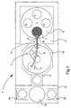
- a station 1 for epitaxial growth treatments of wafers comprises, in general, a reaction chamber 2, a transfer chamber 16, a scrubbing chamber 13, a storage area 17.
- first cassette 14 containing the wafers still to be treated and a second cassette 15 containing the wafers already treated in the station.
- An external robot 18, shown only in a very schematic way in Fig.1, provides, before the treatment, to extract the wafers one by one from cassette 14 and to insert them into scrubbing chamber 13, and, after the treatment, to extract the wafers one by one from scrubbing chamber 13 and to insert them into cassette 15.
- an internal robot 4 is located that provides, before the treatment, to extract the wafers one by one from scrubbing chamber 13 and to insert them into reaction chamber 2, and, after the treatment, to extract the wafers one by one from reaction chamber 2 and to insert them into scrubbing chamber 13.
- a support 9 for the wafers to be treated is located that is usually called “susceptor" in the reactors heated by induction.
- support 9 is able to receive a certain number of wafers, depending also on their diameter; such diameter may reach nowadays twelve inches, i.e. about thirty centimeters, but, in the microelectronic industry, there is a trend to use larger and larger wafers.
- the wafers are seated in pockets 12 formed on the surface of support 9.
- Support 9 is, in general, rotatable, so that robot 4 can place the various wafers in the various pockets always through the same movement.
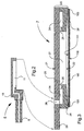
- robot 4 comprises various arms suitably articulated between each other; on a final arm 5 of robot 4 a tool 7 is applied adapted to handle the wafers one by one.
- arm 5 essentially consists of a rigid tube 6 that also acts as suction duct.
- Tube 6 is connected, on one side, to a suction system 3 through a flexible tube 8.
- tube 6 is joined to a plate 10 in order to facilitate the application of tool 7, as will be made clearer in the following.
- tool 7 is useful for handling a wafer 100 in an epitaxial growth station.
- Wafer 100 has a front 101, a back 102 and an edge 103.
- Tool 7 is adapted to be applied to arm 5 (of internal robot 4) provided with suction duct 6 connected to suction system 3.
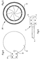
- Tool 7 comprises a disk 20 having an upper side 21 and a lower side 22; lower side 22 is so shaped as to get in contact with wafer 100 only along edge 103 of the wafer; disk 20 is provided internally with a suction chamber 24 that is in communication with the outside of disk 20 through one or more suction holes 25 (in the embodiment shown in the figures these holes are eight) and that is adapted to be put in communication with suction duct 6 through a suction port 26.
- disk 20 is such as to entirely cover wafer 100 and suction holes 25 open to lower side 22 of disk 20, whereby, when wafer 100 is in contact with lower side 22 of disk 20 and suction system 3 is active, wafer 100 is held by tool 7 through suction.
- chamber 24 may take various shapes, for example, cylinder, toroid, cylindrical ring, star, branched; in fact, it has substantially the function of connecting holes 25 to port 26; according to a particularly simplified embodiment of the present invention, tool 7 is provided with only one suction hole and suction chamber 24 substantially simply consists of a suction passageway internal to disk 20 and connecting hole 25 to port 26.
- suction reveals more effective and, therefore, it is possible to reduce it considerably; in such a tool, a reduced suction corresponds to a limited pressure depression applied to the handled wafer and, therefore, to small deformations of the same; additionally, it has been checked that such small deformations are neither permanent nor causing appreciable damages to the structure or to the surfaces of the wafer.
- Such a tool is particularly suitable for being used in epitaxial growth stations with a disk-shaped susceptor as, in these stations, the tool (and also the wafer) is always in a horizontal position; therefore, suction is extremely effective in holding the wafer as its action directly opposes to the weight of the wafer.
- port 26 opens to upper side 21 of disk 20.
- disk 20 may be provided with a plate 23; in this case, port 26 opens to or next to plate 23; typically, plate 23 will be fixed to the corresponding plate of arm 5, for example, through screws.
- disk 20 comprises a shell 28, having outline being substantially ring-shaped and cross-section being substantially U-shaped, and a lid 29, being substantially flat and being substantially circle-shaped, joined to shell 28 in such a way as to form a closed chamber 24 corresponding to the suction chamber and a cavity 27 being substantially cylinder-shaped and corresponding to the suction cavity; shell 28 is so shaped as to get in contact with wafer 100 only along edge 103 of the wafer.
- suction holes 25 open to the lateral walls of cylinder-shaped cavity 27.
- suction holes 25 consist of grooves made on the inner lip of shell 28 at the border with lid 29.
- station 1 for epitaxial growth treatments of wafers, particularly semiconductor material wafers, must comprise a reaction chamber 2, a suction system 3 and a robot 4 for the automatic insertion/extraction of wafers into/from reaction chamber 2; robot 4 must be provided with an arm 5 having a suction duct 6 connected to suction system 3; additionally, it must comprise a tool 7, of the type described above, provided with a suction chamber 24 and adapted to handle a wafer 100; tool 7 must be applied to arm 5 of robot 4 and suction chamber 24 must be in communication with suction duct 6.
- An epitaxial growth station with disk-shaped susceptor would use a tool of the type described above with particular advantage, as already explained.
- suction reveals more effective on the wafer; therefore, it is possible to use a limited suction with beneficial effects on the suction system 3.
- arm 5 of robot 4 essentially consists of a tube, tube 6, this may act at the same time both as support of tool 7 and as suction duct.
- arm 5 of robot 4 comprises a plate 10, joined to one end of tube 6, adapted to be applied to tool 7, and provided with an internal duct 11 that puts tube 6 of arm 5 in communication with suction port 26 of disk 20; this may be better understood making reference to Fig.2 and Fig.6.
- plate 10 of arm 5 is applied to corresponding plate 23 of tool 7 (for example through screws).
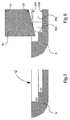
- an advantageous solution to this problem consists in providing that pocket 12 of support 9, adapted to seat wafers 200 to be treated, consist of a first cavity 121 and a second cavity 122 formed within first cavity 121 and having a substantially flat bottom and having a shape and a size corresponding to the wafer to be treated.
- disk 20 touches wafer 200 at its edge 203 without touching front 201, back 202, and even support 9; additionally, edge 203 of wafer 200 is completely masked by the edge of pocket 12.
- the depth of second cavity 122 is preferably smaller than the width of wafer 200 to be treated; as on the market there exist wafers of even quite different width, in this case, a "universal" support has to take the most thick wafer into account.
- first cavity 121 and of second cavity 122 is preferably larger than the width of wafer 200 to be treated; as on the market there exist wafers of even quite different width, in this case, a "universal" support has to take the most thick wafer into account.
- cavity 121 and cavity 122 it is necessary to take into account not only all the possible shapes and sizes of the wafers to be treated but also the shape and size of lower side 22 of disk 20 of tool 7.
- suction system 3 be adapted to realize a suction that depends on the wafer handling phase, in such a way as to apply to the handled wafer, for example, always only the minimum necessary pressure depression.
- suction system 3 be adapted to realize :
- suction values may be used: one for loading the wafers into the reactor and one for unloading the wafers from the reactor.
- suction system 3 be adapted to cause such a pressure depression in the space between disk 20 and handled wafer 100 as to cause no damage to the structure or to the surfaces of handled wafer 100.
- the pressure depression considered is in the range between few millibars to few tens of millibars.
- the control of the suction generated by suction system 3 may be an open-loop control or a closed-loop control.
- Suction system 3 may be of the type based on a pump with vacuum regulator in which the vacuum may be programmed, for example, by a computer.
- this may advantageously be of the type operating by Venturi effect, i.e. of the type based on the pressure depression generated next to a narrowing when a fluid flows; in this case, the system may advantageously be fed with a flow of inert gas.
- suction system 3 may advantageously comprise a Mass Flow Controller [MFC] programmable, for example, by a computer sending "set points"; such controller controls the flow of inert gas and, as a consequence, the generated pressure depression.
- MFC Mass Flow Controller
Landscapes
- Engineering & Computer Science (AREA)
- Container, Conveyance, Adherence, Positioning, Of Wafer (AREA)
- Crystals, And After-Treatments Of Crystals (AREA)
- Physics & Mathematics (AREA)
- Condensed Matter Physics & Semiconductors (AREA)
- General Physics & Mathematics (AREA)
- Manufacturing & Machinery (AREA)
- Computer Hardware Design (AREA)
- Microelectronics & Electronic Packaging (AREA)
- Power Engineering (AREA)
- Chemical Vapour Deposition (AREA)
- Physical Deposition Of Substances That Are Components Of Semiconductor Devices (AREA)
Applications Claiming Priority (3)
| Application Number | Priority Date | Filing Date | Title |
|---|---|---|---|
| IT2001MI002014A ITMI20012014A1 (it) | 2001-09-27 | 2001-09-27 | Utensile per maneggiare fette e stazione per crescita epitassiale |
| ITMI20012014 | 2001-09-27 | ||
| PCT/EP2002/010598 WO2003030222A2 (en) | 2001-09-27 | 2002-09-20 | Tool for handling wafers and epitaxial growth station |
Publications (2)
| Publication Number | Publication Date |
|---|---|
| EP1430516A2 EP1430516A2 (en) | 2004-06-23 |
| EP1430516B1 true EP1430516B1 (en) | 2007-04-18 |
Family
ID=11448442
Family Applications (1)
| Application Number | Title | Priority Date | Filing Date |
|---|---|---|---|
| EP02800104A Expired - Lifetime EP1430516B1 (en) | 2001-09-27 | 2002-09-20 | Tool for handling wafers and epitaxial growth station |
Country Status (10)
| Country | Link |
|---|---|
| US (1) | US6991420B2 (es) |
| EP (1) | EP1430516B1 (es) |
| JP (1) | JP4234007B2 (es) |
| KR (1) | KR20040037094A (es) |
| CN (1) | CN100349253C (es) |
| AT (1) | ATE360259T1 (es) |
| DE (1) | DE60219648T2 (es) |
| ES (1) | ES2283643T3 (es) |
| IT (1) | ITMI20012014A1 (es) |
| WO (1) | WO2003030222A2 (es) |
Families Citing this family (4)
| Publication number | Priority date | Publication date | Assignee | Title |
|---|---|---|---|---|
| CN101199048A (zh) * | 2005-05-26 | 2008-06-11 | Lpe公司 | 用于晶片操纵的真空系统 |
| CN103904013B (zh) * | 2012-12-28 | 2016-12-28 | 上海微电子装备有限公司 | 一种真空吸附装置及吸附测校方法 |
| CN106298618A (zh) * | 2015-06-26 | 2017-01-04 | 北京北方微电子基地设备工艺研究中心有限责任公司 | 晶片传输装置 |
| CN106558523A (zh) * | 2015-09-29 | 2017-04-05 | 奇勗科技股份有限公司 | 非接触式的晶圆搬运装置 |
Family Cites Families (15)
| Publication number | Priority date | Publication date | Assignee | Title |
|---|---|---|---|---|
| US4009785A (en) * | 1974-10-02 | 1977-03-01 | Motorola, Inc. | Fixture and system for handling plate like objects |
| JPS61140432A (ja) * | 1984-12-11 | 1986-06-27 | Shinko Denki Kk | ウエハ−等の保持装置 |
| JPS62106643A (ja) * | 1985-11-05 | 1987-05-18 | Toshiba Corp | 穴開きバキユ−ムウエハチヤツク |
| JPS63228637A (ja) * | 1987-03-18 | 1988-09-22 | Hitachi Ltd | 取付治具 |
| NL8701603A (nl) * | 1987-07-08 | 1989-02-01 | Philips & Du Pont Optical | Vacuuminrichting voor het vastzuigen van werkstukken. |
| JPH0410529A (ja) * | 1990-04-27 | 1992-01-14 | Shin Etsu Handotai Co Ltd | サセプタ及びウエーハ自動脱着装置 |
| US6099056A (en) * | 1996-05-31 | 2000-08-08 | Ipec Precision, Inc. | Non-contact holder for wafer-like articles |
| US5928537A (en) * | 1997-03-14 | 1999-07-27 | Fortune; William S. | Pneumatic pickup tool for small parts |
| US6398621B1 (en) * | 1997-05-23 | 2002-06-04 | Applied Materials, Inc. | Carrier head with a substrate sensor |
| WO1999012074A1 (en) * | 1997-08-29 | 1999-03-11 | Nikon Corporation | Photomask case, conveying device, and conveying method |
| JPH11300608A (ja) * | 1998-04-20 | 1999-11-02 | Nec Corp | 化学機械研磨装置 |
| US6254155B1 (en) * | 1999-01-11 | 2001-07-03 | Strasbaugh, Inc. | Apparatus and method for reliably releasing wet, thin wafers |
| IT1308606B1 (it) * | 1999-02-12 | 2002-01-08 | Lpe Spa | Dispositivo per maneggiare substrati mediante un istema autolivellante a depressione in reattori epistassiali ad induzione con suscettore |
| US6935830B2 (en) * | 2001-07-13 | 2005-08-30 | Tru-Si Technologies, Inc. | Alignment of semiconductor wafers and other articles |
| US6638004B2 (en) * | 2001-07-13 | 2003-10-28 | Tru-Si Technologies, Inc. | Article holders and article positioning methods |
-
2001
- 2001-09-27 IT IT2001MI002014A patent/ITMI20012014A1/it unknown
-
2002
- 2002-09-20 CN CNB028189345A patent/CN100349253C/zh not_active Expired - Lifetime
- 2002-09-20 EP EP02800104A patent/EP1430516B1/en not_active Expired - Lifetime
- 2002-09-20 KR KR10-2004-7004166A patent/KR20040037094A/ko not_active Ceased
- 2002-09-20 JP JP2003533323A patent/JP4234007B2/ja not_active Expired - Lifetime
- 2002-09-20 WO PCT/EP2002/010598 patent/WO2003030222A2/en not_active Ceased
- 2002-09-20 DE DE60219648T patent/DE60219648T2/de not_active Expired - Lifetime
- 2002-09-20 ES ES02800104T patent/ES2283643T3/es not_active Expired - Lifetime
- 2002-09-20 AT AT02800104T patent/ATE360259T1/de not_active IP Right Cessation
-
2004
- 2004-03-26 US US10/813,748 patent/US6991420B2/en not_active Expired - Lifetime
Also Published As
| Publication number | Publication date |
|---|---|
| US6991420B2 (en) | 2006-01-31 |
| JP2005505134A (ja) | 2005-02-17 |
| US20040191029A1 (en) | 2004-09-30 |
| WO2003030222A3 (en) | 2003-11-13 |
| ATE360259T1 (de) | 2007-05-15 |
| JP4234007B2 (ja) | 2009-03-04 |
| EP1430516A2 (en) | 2004-06-23 |
| ES2283643T3 (es) | 2007-11-01 |
| WO2003030222A2 (en) | 2003-04-10 |
| ITMI20012014A1 (it) | 2003-03-27 |
| CN1636264A (zh) | 2005-07-06 |
| ITMI20012014A0 (it) | 2001-09-27 |
| KR20040037094A (ko) | 2004-05-04 |
| CN100349253C (zh) | 2007-11-14 |
| DE60219648T2 (de) | 2007-10-18 |
| DE60219648D1 (de) | 2007-05-31 |
Similar Documents
| Publication | Publication Date | Title |
|---|---|---|
| US6558509B2 (en) | Dual wafer load lock | |
| KR102514879B1 (ko) | 반도체 프로세싱을 위해 원뿔형 웨이퍼 센터링 및 홀딩 디바이스 | |
| TWI823166B (zh) | 電子設備製造裝置、系統及方法中的裝載端口操作 | |
| JP5268126B2 (ja) | デュアルロボット搬送システム | |
| KR101913017B1 (ko) | 프로세싱 챔버 | |
| EP0634787A1 (en) | Subsrate tray and ceramic blade for semiconductor processing apparatus | |
| EP0734056A2 (en) | Ceramic blades for semiconductor processing apparatus | |
| CN111742403A (zh) | 用于处理缩小尺寸的基板的处理套件 | |
| CN111557042B (zh) | 桥接前开式标准舱(foup) | |
| US11211269B2 (en) | Multi-object capable loadlock system | |
| US20190259647A1 (en) | Deposition ring for processing reduced size substrates | |
| WO2015191366A1 (en) | Wafer loading and unloading | |
| EP1430516B1 (en) | Tool for handling wafers and epitaxial growth station | |
| WO2021016115A1 (en) | Multi-object capable loadlock system | |
| JPH09270450A (ja) | 真空処理装置 | |
| JP2009260022A (ja) | 基板処理ユニットおよび基板処理装置 | |
| JPH03155619A (ja) | 真空処理装置 | |
| JP2011238962A (ja) | 載置プレート、基板移載装置および基板処理装置 | |
| KR20250123161A (ko) | 회전 방지 피처를 갖는 캐리어 | |
| JP2007250797A (ja) | 基板処理装置 |
Legal Events
| Date | Code | Title | Description |
|---|---|---|---|
| PUAI | Public reference made under article 153(3) epc to a published international application that has entered the european phase |
Free format text: ORIGINAL CODE: 0009012 |
|
| 17P | Request for examination filed |
Effective date: 20040402 |
|
| AK | Designated contracting states |
Kind code of ref document: A2 Designated state(s): AT BE BG CH CY CZ DE DK EE ES FI FR GB GR IE IT LI LU MC NL PT SE SK TR |
|
| AX | Request for extension of the european patent |
Extension state: AL LT LV MK RO SI |
|
| GRAP | Despatch of communication of intention to grant a patent |
Free format text: ORIGINAL CODE: EPIDOSNIGR1 |
|
| GRAS | Grant fee paid |
Free format text: ORIGINAL CODE: EPIDOSNIGR3 |
|
| GRAA | (expected) grant |
Free format text: ORIGINAL CODE: 0009210 |
|
| AK | Designated contracting states |
Kind code of ref document: B1 Designated state(s): AT BE BG CH CY CZ DE DK EE ES FI FR GB GR IE IT LI LU MC NL PT SE SK TR |
|
| REG | Reference to a national code |
Ref country code: CH Ref legal event code: EP |
|
| REG | Reference to a national code |
Ref country code: IE Ref legal event code: FG4D |
|
| REF | Corresponds to: |
Ref document number: 60219648 Country of ref document: DE Date of ref document: 20070531 Kind code of ref document: P |
|
| REG | Reference to a national code |
Ref country code: CH Ref legal event code: NV Representative=s name: PATENTANWAELTE SCHAAD, BALASS, MENZL & PARTNER AG |
|
| REG | Reference to a national code |
Ref country code: SE Ref legal event code: TRGR |
|
| PGFP | Annual fee paid to national office [announced via postgrant information from national office to epo] |
Ref country code: IE Payment date: 20070913 Year of fee payment: 6 |
|
| PG25 | Lapsed in a contracting state [announced via postgrant information from national office to epo] |
Ref country code: PT Free format text: LAPSE BECAUSE OF FAILURE TO SUBMIT A TRANSLATION OF THE DESCRIPTION OR TO PAY THE FEE WITHIN THE PRESCRIBED TIME-LIMIT Effective date: 20070918 |
|
| ET | Fr: translation filed | ||
| REG | Reference to a national code |
Ref country code: ES Ref legal event code: FG2A Ref document number: 2283643 Country of ref document: ES Kind code of ref document: T3 |
|
| PG25 | Lapsed in a contracting state [announced via postgrant information from national office to epo] |
Ref country code: AT Free format text: LAPSE BECAUSE OF FAILURE TO SUBMIT A TRANSLATION OF THE DESCRIPTION OR TO PAY THE FEE WITHIN THE PRESCRIBED TIME-LIMIT Effective date: 20070418 |
|
| PGFP | Annual fee paid to national office [announced via postgrant information from national office to epo] |
Ref country code: CH Payment date: 20070913 Year of fee payment: 6 Ref country code: FI Payment date: 20070912 Year of fee payment: 6 Ref country code: SK Payment date: 20070822 Year of fee payment: 6 |
|
| PG25 | Lapsed in a contracting state [announced via postgrant information from national office to epo] |
Ref country code: BE Free format text: LAPSE BECAUSE OF FAILURE TO SUBMIT A TRANSLATION OF THE DESCRIPTION OR TO PAY THE FEE WITHIN THE PRESCRIBED TIME-LIMIT Effective date: 20070418 |
|
| PGFP | Annual fee paid to national office [announced via postgrant information from national office to epo] |
Ref country code: CZ Payment date: 20070822 Year of fee payment: 6 |
|
| PG25 | Lapsed in a contracting state [announced via postgrant information from national office to epo] |
Ref country code: BG Free format text: LAPSE BECAUSE OF FAILURE TO SUBMIT A TRANSLATION OF THE DESCRIPTION OR TO PAY THE FEE WITHIN THE PRESCRIBED TIME-LIMIT Effective date: 20070718 Ref country code: DK Free format text: LAPSE BECAUSE OF FAILURE TO SUBMIT A TRANSLATION OF THE DESCRIPTION OR TO PAY THE FEE WITHIN THE PRESCRIBED TIME-LIMIT Effective date: 20070418 |
|
| PLBE | No opposition filed within time limit |
Free format text: ORIGINAL CODE: 0009261 |
|
| STAA | Information on the status of an ep patent application or granted ep patent |
Free format text: STATUS: NO OPPOSITION FILED WITHIN TIME LIMIT |
|
| 26N | No opposition filed |
Effective date: 20080121 |
|
| PG25 | Lapsed in a contracting state [announced via postgrant information from national office to epo] |
Ref country code: GR Free format text: LAPSE BECAUSE OF FAILURE TO SUBMIT A TRANSLATION OF THE DESCRIPTION OR TO PAY THE FEE WITHIN THE PRESCRIBED TIME-LIMIT Effective date: 20070719 Ref country code: MC Free format text: LAPSE BECAUSE OF NON-PAYMENT OF DUE FEES Effective date: 20070930 |
|
| PGFP | Annual fee paid to national office [announced via postgrant information from national office to epo] |
Ref country code: NL Payment date: 20080903 Year of fee payment: 7 |
|
| PG25 | Lapsed in a contracting state [announced via postgrant information from national office to epo] |
Ref country code: EE Free format text: LAPSE BECAUSE OF FAILURE TO SUBMIT A TRANSLATION OF THE DESCRIPTION OR TO PAY THE FEE WITHIN THE PRESCRIBED TIME-LIMIT Effective date: 20070418 |
|
| PGFP | Annual fee paid to national office [announced via postgrant information from national office to epo] |
Ref country code: ES Payment date: 20081021 Year of fee payment: 7 Ref country code: SE Payment date: 20080908 Year of fee payment: 7 |
|
| REG | Reference to a national code |
Ref country code: CH Ref legal event code: PL |
|
| PG25 | Lapsed in a contracting state [announced via postgrant information from national office to epo] |
Ref country code: CZ Free format text: LAPSE BECAUSE OF NON-PAYMENT OF DUE FEES Effective date: 20080920 Ref country code: FI Free format text: LAPSE BECAUSE OF NON-PAYMENT OF DUE FEES Effective date: 20080920 |
|
| PG25 | Lapsed in a contracting state [announced via postgrant information from national office to epo] |
Ref country code: CY Free format text: LAPSE BECAUSE OF FAILURE TO SUBMIT A TRANSLATION OF THE DESCRIPTION OR TO PAY THE FEE WITHIN THE PRESCRIBED TIME-LIMIT Effective date: 20070418 Ref country code: IE Free format text: LAPSE BECAUSE OF NON-PAYMENT OF DUE FEES Effective date: 20080922 |
|
| PG25 | Lapsed in a contracting state [announced via postgrant information from national office to epo] |
Ref country code: LU Free format text: LAPSE BECAUSE OF NON-PAYMENT OF DUE FEES Effective date: 20070920 |
|
| PG25 | Lapsed in a contracting state [announced via postgrant information from national office to epo] |
Ref country code: SK Free format text: LAPSE BECAUSE OF NON-PAYMENT OF DUE FEES Effective date: 20080920 Ref country code: TR Free format text: LAPSE BECAUSE OF FAILURE TO SUBMIT A TRANSLATION OF THE DESCRIPTION OR TO PAY THE FEE WITHIN THE PRESCRIBED TIME-LIMIT Effective date: 20070418 |
|
| PG25 | Lapsed in a contracting state [announced via postgrant information from national office to epo] |
Ref country code: LI Free format text: LAPSE BECAUSE OF NON-PAYMENT OF DUE FEES Effective date: 20080930 Ref country code: CH Free format text: LAPSE BECAUSE OF NON-PAYMENT OF DUE FEES Effective date: 20080930 |
|
| REG | Reference to a national code |
Ref country code: NL Ref legal event code: V1 Effective date: 20100401 |
|
| EUG | Se: european patent has lapsed | ||
| PG25 | Lapsed in a contracting state [announced via postgrant information from national office to epo] |
Ref country code: NL Free format text: LAPSE BECAUSE OF NON-PAYMENT OF DUE FEES Effective date: 20100401 |
|
| PG25 | Lapsed in a contracting state [announced via postgrant information from national office to epo] |
Ref country code: SE Free format text: LAPSE BECAUSE OF NON-PAYMENT OF DUE FEES Effective date: 20090921 |
|
| REG | Reference to a national code |
Ref country code: FR Ref legal event code: ST Effective date: 20110531 |
|
| REG | Reference to a national code |
Ref country code: ES Ref legal event code: FD2A Effective date: 20110711 |
|
| PG25 | Lapsed in a contracting state [announced via postgrant information from national office to epo] |
Ref country code: FR Free format text: LAPSE BECAUSE OF NON-PAYMENT OF DUE FEES Effective date: 20100930 Ref country code: ES Free format text: LAPSE BECAUSE OF NON-PAYMENT OF DUE FEES Effective date: 20110629 |
|
| PG25 | Lapsed in a contracting state [announced via postgrant information from national office to epo] |
Ref country code: ES Free format text: LAPSE BECAUSE OF NON-PAYMENT OF DUE FEES Effective date: 20090921 |
|
| PGFP | Annual fee paid to national office [announced via postgrant information from national office to epo] |
Ref country code: FR Payment date: 20091006 Year of fee payment: 8 |
|
| REG | Reference to a national code |
Ref country code: DE Ref legal event code: R082 Ref document number: 60219648 Country of ref document: DE Representative=s name: HOFFMANN - EITLE PATENT- UND RECHTSANWAELTE PA, DE Ref country code: DE Ref legal event code: R081 Ref document number: 60219648 Country of ref document: DE Owner name: LPE S.P.A., IT Free format text: FORMER OWNER: LPE S.P.A., BOLLATE, IT |
|
| PGFP | Annual fee paid to national office [announced via postgrant information from national office to epo] |
Ref country code: IT Payment date: 20210921 Year of fee payment: 20 |
|
| PGFP | Annual fee paid to national office [announced via postgrant information from national office to epo] |
Ref country code: GB Payment date: 20210927 Year of fee payment: 20 Ref country code: DE Payment date: 20210929 Year of fee payment: 20 |
|
| REG | Reference to a national code |
Ref country code: DE Ref legal event code: R071 Ref document number: 60219648 Country of ref document: DE |
|
| REG | Reference to a national code |
Ref country code: GB Ref legal event code: PE20 Expiry date: 20220919 |
|
| PG25 | Lapsed in a contracting state [announced via postgrant information from national office to epo] |
Ref country code: GB Free format text: LAPSE BECAUSE OF EXPIRATION OF PROTECTION Effective date: 20220919 |