BACKGROUND OF THE INVENTION
Field of the Invention:
-
The present invention relates to an electronic pulse
generation device having a first electrode and a second
electrode formed on an emitter element.
Description of the Related Art:
-
In recent years, electronic pulse generation devices
have electron emitters which have a cathode electrode and
an anode electrode as a basic device. The electronic pulse
generation devices have been used in various applications
such as field emission displays (FEDS) and backlight units.
When the electronic pulse generation devices are applied as
the FEDs, a plurality of electron emitters are arranged in
a two-dimensional array, and a plurality of phosphors are
positioned at predetermined intervals in association with
the respective electron emitters.
-
The conventional examples of the electronic pulse
generation devices are disclosed in Japanese laid-open
patent publication No. 1-311533, Japanese laid-open patent
publication No. 7-147131, Japanese laid-open patent
publication No. 2000-285801, Japanese patent publication
No. 46-20944, and Japanese patent publication No. 44-26125,
for example. All of these disclosed devices are
disadvantageous in that since no dielectric material is
employed in the emitter element, a forming process or a
micromachining process is required between facing
electrodes, a high voltage needs to be applied between the
electrodes to emit electrons, and a panel fabrication
process is complex and entails a high panel fabrication
cost.
-
It has been considered to make an emitter element of a
dielectric material. Various theories about the emission
of electrons from a dielectric material have been presented
in the documents: Yasuoka and Ishii, "Pulsed electron
source using a ferroelectric cathode", J. Appl. Phys., Vol.
68, No. 5, p. 546 - 550 (1999), V.F. Puchkarev, G.A.
Mesyats, "On the mechanism of emission from the
ferroelectric ceramic cathode", J. Appl. Phys., Vol. 78,
No. 9, 1 November, 1995, p. 5633 - 5637, and H. Riege,
"Electron emission from ferroelectrics - a review", Nucl.
Instr. and Meth. A340, p. 80 - 89 (1994).
-
In the conventional example of the electronic pulse
generation device, electrons trapped on the surface of the
dielectric material, at the interface between the
dielectric material and the upper electrode, and in the
dielectric material by the defect level are released
(emitted) when polarization reversal occurs in the
dielectric material. The number of the electrons emitted
by the polarization reversal does not change substantially
depending on the voltage level of the applied voltage
pulse.
-
However, the electron emission is not performed
stably, and the number of emitted electrons is merely tens
of thousands. Therefore, the conventional example of the
electronic pulse generation devices are not suitable for
practical use. Advantages of an electronic pulse
generation device having an emitter element made of a
dielectric material have not been achieved.
SUMMARY OF THE INVENTION
-
The present invention has been made to solve the above
problems, and an object of which is to provide an
electronic pulse generation device made of a dielectric
material, and suitable for practical applications in which
electrons are emitted stably, and the number of the emitted
electrons is controlled easily.
-
The electronic pulse generation device according to
the present invention comprises an emitter element made of
a dielectric material, first and second electrodes in
contact with the emitter element, and means for applying
alternating pulse between the first and second electrodes
to change or reverse polarization of the emitter element.
The emitting element is made of an piezoelectric material,
an anti-ferroelectric material, or an electrostrictive
material.
-
Operation of the electronic pulse generation device
including the emitting element made of a dielectric
material according to the present invention will be
described. Firstly, an alternating pulse is applied
between the first electrode and the second electrode for
causing the first electrode to have a potential lower than
a potential of the second electrode to reverse or change
polarization of at least a portion of the emitter element.
The polarization reversal or the polarization change causes
emission of electrons in the vicinity of the first
electrode. The polarization reversal or the polarization
change generates a locally concentrated electric field on
the first electrode and the positive poles of dipole
moments in the vicinity the first electrode, emitting
primary electrons from the first electrode. The primary
electrons emitted from the first electrode impinge upon the
emitter element, causing the emitter element to emit
secondary electrons.
-
When the first electrode, the emitter element, and a
vacuum atmosphere define a triple point, primary electrons
are emitted from a portion of the first electrode in the
vicinity of the triple point. The emitted primary
electrons impinge upon the emitter element to induce
emission of secondary electrons from the emitter element.
If the first electrode is very thin, having a thickness of
10 nm or less, electrons are emitted from the interface
between the first electrode and the emitter element.
-
The secondary electrons herein include electrons
emitted from the solid emitter element under an energy that
has been generated by a coulomb collision with primary
electrons, Auger electrons, and primary electrons which are
scattered in the vicinity of the surface of the emitter
element (reflected electrons).
-
Since the electrons are emitted according to the
principle as described above, the electron emission is
stably performed, and the number of emitted electrons would
reach 2 billion or more. Thus, the electronic pulse
generation device is advantageously used in the practical
applications. The number of emitted electrons is increased
substantially proportional to the voltage between the first
electrode and the second electrode. Thus, the number of
the emitted electrons can be controlled easily.
-
When the electronic pulse generation device is used as
a pixel of a display, a third electrode is provided above
the emitter element at a position facing the first
electrode. The third electrode is coated with a phosphor
layer. Some of the emitted electrons are guided to the
third electrode to excite the phosphor layer to emit
fluorescent light from the phosphor layer to the outside.
-
The third electrode may be provided such that the
third electrode faces the emitter element, and a vacuum
space is present between the emitter element and the third
electrode. Means for applying positive direct bias voltage
to the third electrode may be provided so that electrons
are emitted from the emitter element toward the third
electrode intermittently.
-
In the means for applying alternating pulse, the
polarization of the emitter element in one direction may be
performed by applying a first voltage between the first
electrode and the second electrode for causing the first
electrode to have a potential higher than a potential of
the second electrode in a first period, and
the polarization reversal or polarization change of
the emitter element for emitting electrons may be performed
by applying a second voltage between the first electrode
and the second electrode for causing the first electrode to
have a potential lower than a potential of the second
electrode in a second period.
-
In the present invention, the first electrode and the
second electrode may be formed in contact with the emitter
element; and
a slit may be formed between the first electrode and
the second electrode.
-
In this case, polarization reversal or polarization
change may occur in an electric field E applied to the
emitter element represented by E= Vak/d, where d is a width
of the slit, and Vak is a voltage between the first
electrode and the second electrode.
-
In the present invention, the first electrode may be
formed on a first surface of the emitter element, and the
second electrode may be formed on a second surface of the
emitter element. In this case, polarization reversal or
polarization change may occur in an electric field E
applied to the emitter element represented by E= Vak/h,
where h is a thickness of the emitter element between the
first electrode and the second electrode, and Vak is a
voltage between the first electrode and the second
electrode.
-
Preferably, the voltage Vak between the first
electrode and the second electrode is less than a
dielectric breakdown voltage of the emitter element.
-
The above and other objects, features, and advantages
of the present invention will become more apparent from the
following description of preferred embodiments when taken
in conjunction with the accompanying drawings.
BRIEF DESCRIPTION OF THE DRAWINGS
-
- FIG. 1 is a view showing an electronic pulse
generation device according to a first embodiment of the
present invention;
- FIG. 2 is a plan view showing electrodes of the
electronic pulse generation device according to the first
embodiment of the present invention;
- FIG. 3 is a plan view showing electrodes in a first
modification of the electronic pulse generation device
according to the first embodiment of the present invention;
- FIG. 4 is a plan view showing electrodes in a second
modification of the electronic pulse generation device
according to the first embodiment of the present invention;
- FIG. 5 is a plan view showing electrodes in a third
modification of the electronic pulse generation device
according to the first embodiment of the present invention;
- FIG. 6 is a waveform diagram showing a drive voltage
outputted from a pulse generation source;
- FIG. 7 is a view illustrative of operation when a
first voltage is applied between the cathode electrode and
the anode electrode;
- FIG. 8 is a view illustrative of operation when a
second voltage is applied between the cathode electrode and
the anode electrode;
- FIG. 9 is a view showing an operation in which
electron emission is stopped automatically when a surface
of an emitter element is charged negatively;
- FIG. 10 is a view showing relationship between the
energy of the emitted secondary electrons and the number of
emitted secondary electrons;
- FIG. 11A is a waveform diagram showing an example
(rectangular pulse waveform) of the drive voltage;
- FIG. 11B is a waveform showing the change of the
voltage between the anode electrode and the cathode
electrode of the electronic pulse generation device
according to the first embodiment of the present invention;
- FIG. 12 is a view showing a polarization-electric
field characteristic curve of a piezoelectric material;
- FIG. 13 is a waveform diagram showing changes in the
drive voltage applied between the cathode electrode and the
anode electrode, a collector current flowing through a
collector electrode, and a voltage between the cathode
electrode and the anode electrode in an electronic pulse
generation device according to the first specific example;
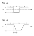
- FIG. 14A is a waveform diagram showing an example
(rectangular pulse waveform) of the drive voltage;
- FIG. 14B is a waveform diagram showing another example
(pulse waveform having a ramp falling edge) of the drive
voltage;
- FIG. 15 is a view showing a polarization-electric
field characteristic curve of an anti-ferroelectric
material;
- FIG. 16 is a waveform diagram showing changes in the
drive voltage applied between the cathode electrode and the
anode electrode, a collector current flowing the collector
electrode, and the voltage between the cathode electrode
and the anode electrode in an electronic pulse generation
device according to the second specific example;
- FIG. 17 is a view showing a polarization-electric
field characteristic curve of an electrostrictive material;
- FIG. 18 is a waveform diagram showing changes in the
drive voltage applied between the cathode electrode and the
anode electrode, a collector current flowing the collector
electrode, and the voltage between the cathode electrode
and the anode electrode in an electronic pulse generation
device according to the third specific example;
- FIG. 19 is a view showing an electronic pulse
generation device according to a second embodiment;
- FIG. 20 is a view showing an electronic pulse
generation device according to a third embodiment;
- FIG. 21 is a plan view showing electrodes of the
electronic pulse generation device according to the third
embodiment of the present invention;
- FIG. 22 is a view illustrative of operation when a
first voltage is applied between the cathode electrode and
the anode electrode;
- FIG. 23A is a view illustrative of operation (emission
of primary electrons) when a second voltage is applied
between the cathode electrode and the anode electrode;
- FIG. 23B is a view illustrative of operation of
emission of secondary electrons caused by the emission of
primary electrons;
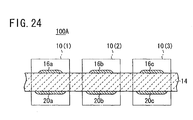
- FIG. 24 is a view showing a first example in which a
plurality of electronic pulse generation devices are
combined;
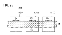
- FIG. 25 is a view showing a second example in which a
plurality of electronic pulse generation devices are
combined;
- FIG. 26 is a view showing a third example in which a
plurality of electronic pulse generation devices are
combined;
- FIG. 27 is a view showing a fourth example in which a
plurality of electronic pulse generation devices are
combined;
- FIG. 28 is a view showing a fifth example in which a
plurality of electronic pulse generation devices are
combined; and
- FIG. 29 is a view showing a sixth example in which a
plurality of electronic pulse generation devices are
combined.
-
DESCRIPTION OF THE PREFERRED EMBODIMENTS
-
Electronic pulse generation devices according to
embodiments of the present invention will be described
below with reference to FIGS. 1 through 29.
-
The electronic pulse generation devices according to
embodiments of the present invention can be used in
displays, electron beam irradiation apparatus, light
sources, alternatives to LEDs, and apparatus for
manufacturing electronic parts.
-
Electron beams in electron beam irradiation apparatus
have a high energy and a good absorption capability in
comparison with ultraviolet rays in ultraviolet ray
irradiation apparatus that are presently in widespread use.
The electronic pulse generation devices are used to
solidify insulating films in superposing wafers for
semiconductor devices, harden printing inks without
irregularities for drying prints, and sterilize medical
devices while being kept in packages.
-
The electronic pulse generation devices are also used
as high-luminance, high-efficiency light sources such as a
projector having a high pressure mercury lamp. The
electronic pulse generation device according to the present
embodiment is suitably used as a light source. The light
source using the electronic pulse generation device
according to the present embodiment is compact, has a long
service life, has a fast response speed for light emission.
The electronic pulse generation device does not use any
mercury, and the electronic pulse generation device is
environmentally friendly.
-
The electronic pulse generation devices are also used
as alternatives to LEDs in indoor lights, automobile lamps,
surface light sources for traffic signal devices, chip
light sources, and backlight units for traffic signal
devices, small-size liquid-crystal display devices for
cellular phones.
-
The electronic pulse generation devices are also used
in apparatus for manufacturing electronic parts, including
electron beam sources for film growing apparatus such as
electron beam evaporation apparatus, electron sources for
generating a plasma (to activate a gas or the like) in
plasma CVD apparatus, and electron sources for decomposing
gases. The electronic pulse generation devices are also
used as vacuum micro devices such as high speed switching
devices operated at a frequency on the order of Tera-Hz,
and large current outputting devices. Further, the
electronic pulse generation devices are used suitably as
parts of printers, such as light emitting devices for
emitting light to a photosensitive drum, and electron
sources for charging a dielectric material.
-
The electronic pulse generation devices are also used
as electronic circuit devices including digital devices
such as switches, relays, and diodes, and analog devices
such as operational amplifiers. The electronic pulse
generation devices are used for realizing a large current
output, and a high amplification ratio.
-
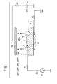
As shown in FIG. 1, an electronic pulse generation
device 10A according to a first embodiment of the present
invention has an emitter section (emitter element) 14
having a plate shape, a first electrode (a cathode
electrode) 16 formed on a front surface of the emitter
section 14, a second electrode (an anode electrode) 20
formed on a back surface of the emitter section 14, and a
pulse generation source (means for applying alternating
pulse) 22 which applies a drive voltage Va between the
cathode electrode 16 and the anode electrode 20 through a
resistor R1.
-
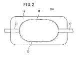
In an example shown in FIG. 1, the anode electrode 20
is connected to GND (ground) and hence set to a zero
potential. However, the anode electrode 20 may be set to a
potential other than the zero potential. As shown in FIG.
2, the drive voltage Va is applied between the cathode
electrode 16 and the anode electrode 20 through a lead
electrode 17 extending from the cathode electrode 16 and a
lead electrode 21 extending from the anode electrode 20,
for example.
-
For using the electronic pulse generation device 10A
as a pixel of a display, a collector electrode 24 is
positioned above the cathode electrode 16, and the
collector electrode 24 is coated with a phosphor layer 28.
The collector electrode 24 is connected to a bias voltage
source 102 (bias voltage Vc) through a resistor R3.
-
The electronic pulse generation device 10A according
to the first embodiment of the present invention is placed
in a vacuum space. As shown in FIG. 1, the electronic
pulse generation device 10A has electric field
concentration point A. The point A can be defined as a
triple point where the cathode electrode 16, the emitter
section 14, and the vacuum are present at one point.
-
The vacuum level in the atmosphere is preferably in
the range from 102 to 10-6 Pa and more preferably in the
range from 10-3 to 10-5 Pa.
-
The range of the vacuum level is determined for the
following reason. In a lower vacuum, (1) many gas
molecules would be present in the space, and a plasma can
easily be generated and, if the plasma were generated
excessively, many positive ions would impinge upon the
cathode electrode 16 and damage the cathode electrode 16,
and (2) emitted electrons would impinge upon gas molecules
prior to arrival at the collector electrode 24, failing to
sufficiently excite the phosphor layer 28 with electrons
that are sufficiently accelerated by the collector
potential (Vc).
-
In a higher vacuum, though electrons are smoothly
emitted from the electric field concentration point A,
structural body supports and vacuum seals would be large in
size, posing difficulty in making a small electronic pulse
generation device.
-
The emitter section 14 is made of a dielectric
material. The dielectric material should preferably have a
high relative dielectric constant (relative permittivity),
e.g., a dielectric constant of 1000 or higher. Dielectric
materials of such a nature may be ceramics including barium
titanate, lead zirconate, lead magnesium niobate, lead
nickel niobate, lead zinc niobate, lead manganese niobate,
lead magnesium tantalate, lead nickel tantalate, lead
antimony stannate, lead titanate, lead magnesium
tungstenate, lead cobalt niobate, etc. or a material whose
principal component contains 50 weight % or more of the
above compounds, or such ceramics to which there is added
an oxide of lanthanum, calcium, strontium, molybdenum,
tungsten, barium, niobium, zinc, nickel, manganese, or the
like, or a combination of these materials, or any of other
compounds.
-
For example, a two-component material nPMN-mPT (n, m
represent molar ratios) of lead magnesium niobate (PMN) and
lead titanate (PT) has its Curie point lowered for a larger
relative dielectric constant at room temperature if the
molar ratio of PMN is increased.
-
Particularly, a dielectric material where n =
0.85 - 1.0 and m = 1.0 - n is preferable because its relative
dielectric constant is 3000 or higher. For example, a
dielectric material where n = 0.91 and m = 0.09 has a
relative dielectric constant of 15000 at room temperature,
and a dielectric material where n = 0.95 and m = 0.05 has a
relative dielectric constant of 20000 at room temperature.
-
For increasing the relative dielectric constant of a
three-component dielectric material of lead magnesium
niobate (PMN), lead titanate (PT), and lead zirconate (PZ),
it is preferable to achieve a composition close to a
morphotropic phase boundary (MPB) between a tetragonal
system and a quasi-cubic system or a tetragonal system and
a rhombohedral system, as well as to increase the molar
ratio of PMN. For example, a dielectric material where
PMN : PT : PZ = 0.375 : 0.375 : 0.25 has a relative
dielectric constant of 5500, and a dielectric material
where PMN : PT : PZ = 0.5 : 0.375 : 0.125 has a relative
dielectric constant of 4500, which is particularly
preferable. Furthermore, it is preferable to increase the
dielectric constant by introducing a metal such as platinum
into these dielectric materials within a range to keep them
insulative. For example, a dielectric material may be
mixed with 20 weight % of platinum.
-
As described above, the emitter section 14 may be
formed of a piezoelectric/electrostrictive layer or an
anti-ferroelectric layer. If the emitter section 14 is a
piezoelectric/electrostrictive layer, then it may be made
of ceramics such as lead zirconate, lead magnesium niobate,
lead nickel niobate, lead zinc niobate, lead manganese
niobate, lead magnesium tantalate, lead nickel tantalate,
lead antimony stannate, lead titanate, barium titanate,
lead magnesium tungstenate, lead cobalt niobate, or the
like, or a combination of any of these materials.
-
The emitter section 14 may be made of chief components
including 50 weight % or more of any of the above
compounds. Of the above ceramics, the ceramics including
lead zirconate is most frequently used as a constituent of
the piezoelectric/electrostrictive layer of the emitter
section 14.
-
If the piezoelectric/electrostrictive layer is made of
ceramics, then oxides of lanthanum, calcium, strontium,
molybdenum, tungsten, barium, niobium, zinc, nickel,
manganese, or the like, or a combination of these
materials, or any of other compounds may be added to the
ceramics.
-
For example, the piezoelectric/electrostrictive layer
should preferably be made of ceramics including as chief
components lead magnesium niobate, lead zirconate, and lead
titanate, and also including lanthanum and strontium.
-
The piezoelectric/electrostrictive layer may be dense
or porous. If the piezoelectric/electrostrictive layer is
porous, then it should preferably have a porosity of 40 %
or less.
-
If the emitter section 14 is formed of an anti-ferroelectric
layer, then the anti-ferroelectric layer may
be made of lead zirconate as a chief component, lead
zirconate and lead stannate as chief components, lead
zirconate with lanthanum oxide added thereto, or lead
zirconate and lead stannate as components with lead
zirconate and lead niobate added thereto.
-
The anti-ferroelectric layer may be porous. If the
anti-ferroelectric layer is porous, then it should
preferably have a porosity of 30 % or less.
-
Strontium bismuthate tantalate is used suitably for
the emitter section 14. The emitter section 14 made of
strontium bismuthate tantalate is not damaged by the
polarization reversal easily. For preventing damages due
to the polarization reversal, lamellar ferroelectric
compounds represented by a general formula
(BiO2)2+(Am-1BmO3m+1)2-are used. The ionized metal A includes Ca2+, Sr2+,
Ba2+, Pb2+, Bi3+, La3+, and the ionized metal B includes Ti4+,
Ta5+, Nb5+.
-
Piezoelectric/electrostrictive/anti-ferroelectric
ceramics is mixed with glass components such as lead
borosilicate glass or other compounds having a low melting
point such as bismuth oxide to lower the firing
temperature.
-
The emitter section 14 may be made of a material which
does not contain any lead, i.e., made of a material having
a high melting temperature, or a high evaporation
temperature. Thus, the emitter section 14 is not damaged
easily when electrons or ions impinge upon the emitter
section 14.
-
The thickness h (see FIG. 1) of the emitter section 14
between the cathode electrode 16 and the anode electrode 20
is determined so that polarization reversal or polarization
change occurs in the electric field E represented by E=
Vak/h (Vak is a voltage measured between the cathode
electrode 16 and the anode electrode 20 when the drive
voltage Va outputted from the pulse generation source 22 is
applied between the cathode electrode 16 and the anode
electrode 20). When the thickness h is small, the
polarization reversal or polarization change occurs at a
low voltage, and electrons are emitted at the low voltage
(e.g., less than 100V).
-
The cathode electrode 16 is made of materials
described below. The cathode electrode 16 should
preferably be made of a conductor having a small sputtering
yield and a high evaporation temperature in vacuum. For
example, materials having a sputtering yield of 2.0 or less
at 600 V in Ar+ and an evaporation temperature of 1800 K or
higher at an evaporation pressure of 1.3 × 10⁻³ Pa are
preferable. Such materials include platinum, molybdenum,
tungsten, etc. Further, the cathode electrode 18 is made
of a conductor which is resistant to a high-temperature
oxidizing atmosphere, e.g., a metal, an alloy, a mixture of
insulative ceramics and a metal, or a mixture of insulative
ceramics and an alloy. Preferably, the cathode electrode
16 should be composed chiefly of a precious metal having a
high melting point, e.g., platinum, iridium, palladium,
rhodium, molybdenum, or the like, or an alloy of silver and
palladium, silver and platinum, platinum and palladium, or
the like, or a cermet of platinum and ceramics. Further
preferably, the cathode electrode 16 should be made of
platinum only or a material composed chiefly of a platinum-base
alloy. The electrode should preferably be made of
carbon or a graphite-base material, e.g., diamond thin
film, diamond-like carbon, or carbon nanotube. Ceramics to
be added to the electrode material should preferably have a
proportion ranging from 5 to 30 volume %.
-
Further, preferably, organic metal pastes which
produce a thin film after firing, such as platinum resinate
paste are used. Further, for preventing damages due to
polarization reversal, oxide electrode is used. The oxide
electrode is made of any of ruthenium oxide, iridium oxide,
strontium ruthenate, La1-xSrxCoO3 (e.g., x=0.3 or 0.5),
La1-xCaxMnO3, La1-xCaxMn1-yCoyO3 (e.g, x=0.2, y=0.05).
Alternatively, the oxide electrode is made by mixing any of
these materials with platinum resinate paste, for example.
-
The cathode electrode 16 may be made of any of the
above materials by an ordinary film forming process which
may be any of various thick-film forming processes
including screen printing, spray coating, dipping, coating,
electrophoresis, etc., or any of various thin-film forming
processes including sputtering, an ion beam process, vacuum
evaporation, ion plating, chemical vapor deposition (CVD),
plating, etc. Preferably, the cathode electrode 18 is made
by any of the above thick-film forming processes.
-
The cathode electrode 16 may have an oval shape as
shown in a plan view of FIG. 2, or a ring shape like an
electronic pulse generation device 10Aa of a first
modification as shown in a plan view of FIG. 3.
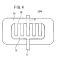
Alternatively, the cathode electrode 16 may have a comb
teeth shape like an electronic pulse generation device 10Ab
of a second modification as shown in FIG. 4.
-
When the cathode electrode 16 having a ring shape or a
comb teeth shape in a plan view is used, the number of
triple points (electric field concentration points A) of
the cathode electrode 16, the emitter section 14, and the
vacuum is increased, and the efficiency of electron
emission is improved. Further, electric capacitance is
suitably reduced, and electric power consumption is
reduced.
-
Preferably, the cathode electrode 16 has a thickness
tc (see FIG. 1) of 20 µm or less, or more preferably 5 µm
or less. The cathode electrode 16 may have a thickness tc
of 100 nm or less. In particular, an electronic pulse
generation device 10Ac of a third modification shown in
FIG. 5 is very thin, having a thickness tc of 10 nm or
less. In this case, electrons are emitted from the
interface between the cathode electrode 16 and the emitter
section 14, and thus, the efficiency of electron emission
is further improved.
-
The anode electrode 20 is made of the same material by
the same process as the cathode electrode 16. Preferably,
the anode electrode 20 is made by any of the above thick-film
forming processes. Preferably, the anode electrode 20
has a thickness tc of 20 µm or less, or more preferably 5
µm or less.
-
Each time the emitter section 14, the cathode
electrode 16, or the anode electrode 20 is formed, the
assembly is heated (sintered) into an integral structure.
Depending on the process by which the cathode electrode 16
and the anode electrode 20 are formed, they may not be
heated (sintered) so as to be integrally combined together.
-
The sintering process for integrally combining the
emitter section 14, the cathode electrode 16, and the anode
electrode 20 may be carried out at a temperature ranging
from 500 to 1400°c, preferably from 1000 to 1400°C. For
heating the emitter section 14 which is in the form of a
film, the emitter section 14 should be sintered together
with its evaporation source while their atmosphere is being
controlled.
-
The emitter section 14 may be covered with an
appropriate member for preventing the surface thereof from
being directly exposed to the sintering atmosphere when the
emitter section 14 is sintered.
-
The principles of electron emission of the electronic
pulse generation device 10A will be described below with
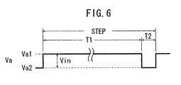
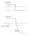
reference to FIGS. 1, and 6 through 11B. As shown in FIG.
6, The drive voltage Va has the waveform of an alternating
pulse. The drive voltage Va outputted from the pulse
generation source 22 has repeated steps each including a
period in which a first voltage Va1 is outputted
(preparatory period T1) and a period in which a second
voltage Va2 is outputted (electron emission period T2).
The first voltage Va1 is such a voltage that the potential
of the cathode electrode 16 is higher than the potential of
the anode electrode 20, and the second voltage Va2 is such
a voltage that the potential of the cathode electrode 16 is
lower than the potential of the anode electrode 20. The
amplitude Vin of the drive voltage Va can be defined as the
difference (= Va1 - Va2) between the first voltage Va1 and
the second voltage Va2.
-
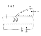
The preparatory period T1 is a period in which the
first voltage Va1 is applied between the cathode electrode
16 and the anode electrode 20 to polarize the emitter
section 14, as shown in FIG. 7. The first voltage Va1 may
be a DC voltage, as shown in FIG. 6, but may be a single
pulse voltage or a succession of pulse voltages. The
preparatory period T1 should preferably be longer than the
electron emission period T2 for sufficient polarization.
For example, the preparatory period T1 should preferably be
100 µsec. or longer. This is because the absolute value of
the first voltage Va1 for polarizing the emitter section 14
is smaller than the absolute value of the second voltage
Va2 to reduce the power consumption at the time of applying
the first voltage Va1, and to prevent the damage of the
cathode electrode 16.
-
Preferably, the voltage levels of the first voltage
Va1 and the second voltage Va2 are determined so that the
polarization to the positive polarity and the negative
polarity can be performed reliably. For example, if the
dielectric material of the emitter section 14 has a
coercive voltage, preferably, the absolute values of the
first voltage Va1 and the second voltage Va2 are the
coercive voltage or higher.
-
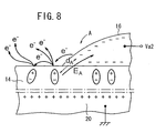
The electron emission period T2 is a period in which
the second voltage Va2 is applied between the cathode
electrode 16 and the anode electrode 20. When the second
voltage Va2 is applied between the cathode electrode 16 and
the anode electrode 20, as shown in FIG. 8, the
polarization of at least a part of the emitter section 16
is reversed or changed. Specifically, the polarization
reversal or the polarization change occurs at a portion of
the emitter section 14 which is underneath the cathode
electrode 16, and a portion of the emitter section 14 which
is exposed near the cathode electrode 16. The polarization
likely to changes at the exposed portion near the cathode
electrode 16. Because of the polarization reversal or the
polarization change, a locally concentrated electric field
is generated on the cathode electrode 16 and the positive
poles of dipole moments in the vicinity thereof, emitting
primary electrons from the cathode electrode 16. The
primary electrons emitted from the cathode electrode 16
impinge upon the emitter section 14, causing the emitter
section 14 to emit secondary electrons.
-
With the electronic pulse generation device 10A of the
first embodiment having the triple point A where the
cathode electrode 16, the emitter section 14, and the
vacuum are present at one point, primary electrons are
emitted from the cathode electrode 16 near the triple point
A, and the primary electrons thus emitted from the triple
point A impinge upon the emitter section 14, causing the
emitter section 14 to emit secondary electrons. If the
thickness of the cathode electrode 16 is very small (up to
10 nm), then electrons are emitted from the interface
between the cathode electrode 16 and the emitter section
14.
-
Operation by application of the negative voltage Va2
will be described in detail below.
-
When the second voltage Va2 is applied between the
cathode electrode 16 and the anode electrode 20, electrons
are emitted from the emitter section 14. Specifically, in
the emitter section 14, dipole moments near the cathode
electrode 16 are charged when the polarization of the
emitter section has been reversed or changed. Thus,
emission of the electrons occurs.
-
A local cathode is formed in the cathode electrode 16
in the vicinity of the interface between the cathode
electrode 16 and the emitter section 14, and positive poles
of the dipole moments charged in the area of the emitter
section 14 near the cathode electrode 16 serve as a local
anode which causes the emission of electrons from the
cathode electrode 16. Some of the emitted electrons are
guided to the collector electrode 24 (see FIG. 1) to excite
the phosphor layer 28 to emit fluorescent light from the
phosphor layer 28 to the outside. Further, some of the
emitted electrons impinge upon the emitter section 14 to
cause the emitter section 14 to emit secondary electrons.
The secondary electrons are guided to the collector
electrode 24 to excite the phosphor layer 28.
-
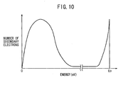
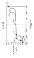
A distribution of emitted secondary electrons will be
described below with reference to FIG. 10. As shown in
FIG. 10, most of the secondary electrons have an energy
level near zero. When the secondary electrons are emitted
from the surface of the emitter section 14 into the vacuum,
they move according to only an ambient electric field
distribution. Specifically, the secondary electrons are
accelerated from an initial speed of about 0 (m/sec)
according to the ambient electric field distribution.
Therefore, as shown in FIG. 1, if an electric field Ea is
generated between the emitter section 14 and the collector
electrode 24, the secondary electrons has their emission
path determined along the electric field Ea. Therefore,
the electronic pulse generation device 10A can serve as a
highly straight electron source. The secondary electrons
which have a low initial speed are electrons which are
emitted from the solid emitter section 14 under an energy
that has been generated by a coulomb collision with primary
electrons.
-
As can be seen from FIG. 10, secondary electrons
having an energy level which corresponds to the energy E0 of
primary electrons are emitted. These secondary electrons
are primary electrons that are emitted from the cathode
electrode 16 and scattered in the vicinity of the surface
of the emitter section 14 (reflected electrons). The
secondary electrons referred herein include both the
reflected electrons and Auger electrons.
-
If the thickness of the cathode electrode 16 is very
small (up to 10 nm), then primary electrons emitted from
the cathode electrode 16 are reflected by the interface
between the cathode electrode 16 and the emitter section
14, and directed toward the collector electrode 24.
-
The intensity EA of the electric field at the electric
field concentration point A satisfies the equation EA =
V(la, lk)/dA where V(la, lk) represents the potential
difference between the local anode and the local cathode,
and dA represents the distance between the local anode and
the local cathode. Because the distance dA between the
local anode and the local cathode is very small, it is
possible to easily obtain the intensity EA of the electric
field which is required to emit electrons (the large
intensity EA of the electric field is indicated by the
solid-line arrow in FIG. 8). This ability to easily obtain
the intensity EA of the electric field leads to a reduction
in the voltage Vak.
-
As the electron emission from the cathode electrode 16
progresses, floating atoms of the emitter section 14 which
are evaporated due to the Joule heat are ionized into
positive ions and electrons by the emitted electrons. The
electrons generated by the ionization ionize the atoms of
the emitter section 14. Therefore, the electrons are
increased exponentially to generate a local plasma in which
the electrons and the positive ions are neutrally present.
The positive ions generated by the ionization may impinge
upon the cathode electrode 16, possibly damaging the
cathode electrode 16.
-
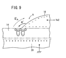
In the electronic pulse generation device 10A
according to the first embodiment, as shown in FIG. 9, the
electrons emitted from the cathode electrode 16 are
attracted to the positive poles, which are present as the
local anode, of the dipole elements in the emitter section
14, negatively charging the surface of the emitter section
14 near the cathode electrode 16. As a result, the factor
for accelerating the electrons (the local potential
difference) is lessened, and any potential for emitting
secondary electrons is eliminated, further progressively
negatively charging the surface of the emitter section 14.
-
Therefore, the positive polarity of the local anode
provided by the dipole moments is weakened, and the
intensity EA of the electric field between the local anode
and the local cathode is reduced (the small intensity EA of
the electric field is indicated by the broken-line arrow in
FIG. 9). Thus, the electron emission is stopped.
-
As shown in FIG. 11A, the drive voltage Va applied
between the cathode electrode 16 and the anode electrode 20
has a positive voltage Va1 of 50 V, and a negative voltage
va2 of -100V. The change ΔVak of the voltage between the
cathode electrode 16 and the anode electrode 20 at the time
P1 (peak) the electrons are emitted is 20V or less (about
10 V in the example of FIG. 11B), and very small.
Consequently, almost no positive ions are generated, thus
preventing the cathode electrode 16 from being damaged by
positive ions. This arrangement is thus effective to
increase the service life of the electronic pulse
generation device 10A.
-
After the electron emission period T2, the preparatory
period T1 is repeated in the next cycle. In the
preparatory period T1 of the next cycle, the cathode
electrode 16 of the electronic pulse generation device 10A
has a potential higher than a potential of the anode
electrode 20 again (the negative poles of dipole moments
appear on the surface of the emitter section 14 again).
Therefore, the negative charge on the emitter section 14
which caused interruption of the electron emission is
eliminated. By application of the alternating pulse, a
sufficient level of electric field intensity EA can be
maintained in every electron emission period T2, and the
electron emission can be carried out stably.
-
Preferably, the dielectric breakdown voltage of the
emitter section 14 is at least 10kV/mm or higher. In the
embodiment, when the thickness h of the emitter section 14
is 20 µm, even if the drive voltage of -100V is applied
between the cathode electrode 16 and the anode electrode
20, the emitter section 14 does not break down
dielectrically.
-
The emitter section 14 is likely to be damaged when
electrons emitted from the emitter section 14 impinge upon
the emitter section 14 again or when ionization occurs near
the surface of the emitter section 14. Due to the damages
to the crystallization, the mechanical strength and the
durability of the emitter section 14 are likely to be
lowered.
-
In order to avoid the problem, preferably, the emitter
section 14 is made of a dielectric material having a high
evaporation temperature in vacuum. For example, the
emitter section 14 may be made of BaTiO3 which does not
include Pb. Thus, the emitter section 14 is not evaporated
into floating atoms easily due to the Joule heat, and the
ionization by the emitted electrons is prevented.
Therefore, the surface of the emitter section 14 is
effectively protected.
-
The pattern or the potential of the collector
electrode 24 may be changed suitably depending on the
application. If a control electrode (not shown) or the
like is provided between the emitter section 14 and the
collector electrode 24 for arbitrarily setting the electric
field distribution between the emitter section 14 and the
collector electrode 24, the emission path of the emitted
secondary electrons can be controlled easily. Thus, it is
possible to change the size of the electron beam by
converging and expanding the electron beam, and to change
the shape of the electron beam easily.
-
As described above, the electron source emitting a
straight electron beam is produced, and the emission path
of emitted secondary electrons is controlled easily.
Therefore, the electronic pulse generation device 10A
according to the first embodiment can be utilized
advantageously as a pixel of a display with an aim to
decrease the pitch between the pixels.
-
Next, three specific examples of the electronic pulse
generation device 10A according to the first embodiment of
the present invention will be described.
-
First, the electronic pulse generation device 10A1
according to the first specific example will be described.
The electronic pulse generation device 10A1 according to a
first specific example has substantially the same structure
as the electronic pulse generation device 10A according to
the first embodiment described above, but differs from the
electronic pulse generation device 10A in that the emitter
section 14 is made of a piezoelectric material.
-
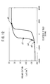
FIG. 7 shows a polarization-electric field
characteristic curve of the piezoelectric material of the
emitter section 14. In FIG. 12, a hysteresis loop is shown
around a level where the electric field E= 0 (V/mm).
-
The hysteresis loop from a point p1, a point p2, to a
point p3 will be described. When a positive electric field
is applied to the piezoelectric material at the point p1,
the piezoelectric material is polarized substantially in
one direction. Thereafter, when the electric field is
negatively increased to a level of a coercive field (about
-700V/mm) at the point p2, polarization reversal starts to
occur. At the point p3, polarization reversal is carried
out completely.
-
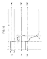
In the first specific example, as shown in FIG. 13, a
first voltage Va1 is applied between the cathode electrode
16 and the anode electrode 20, and a positive electric
field (about 1000V/mm) is applied to the emitter section 14
in the preparatory period T1. At this time, as shown in
the polarization-electric field characteristic curve in
FIG. 12, the emitter section 14 is polarized in one
direction.
-
Thereafter, in the electron emission period T2 shown
in FIG. 13, when a second voltage Va2 is applied between
the cathode electrode 16 and the anode electrode 20, for
rapidly changing the electric field to a level (e.g., about
-1000V/mm) beyond the level of the coercive field, electron
emission starts to occur at the point p4, before the point
p3 shown in FIG. 12. As shown in FIG. 13, within a certain
period tc1 (10 µsec or less in this example) from the
beginning of the electron emission period T2, at a the time
P1 when the voltage Vak between the cathode electrode 16
and the anode electrode 20 is a peak, small voltage drop
occurs. The electron emission occurs at the time P1
(peak). At the time P1 (peak), a current (collector
current Ic) flows the collector electrode 24 rapidly, i.e.,
the emitted electrons are collected by the collector
electrode 24.
-
As described above, the second voltage Va2 is applied
between the cathode electrode 16 and the anode electrode
20, for causing emission of the secondary electrons from
the emitter section 14 or from the interface between the
cathode electrode 16 and the emitter section 14.
-
After the electron emission, the voltage Vak between
the cathode electrode 16 and the anode electrode 20 is
increased again by the second voltage Va2 applied to the
cathode electrode 16. However, since the voltage drop at
the time of the electron emission is small (about 20V), the
electron emission does not occur after the first electron
emission.
-
In the electronic pulse generation device 10A1
according to the first specific example, the electric field
beyond the level of the coercive field is rapidly applied
to the emitter section 14 which is polarized in one
direction. Therefore, the electrons are emitted
efficiently, and the electronic pulse generation device
10A1 can be utilized easily in displays or light sources.
-
The electric field for inducing electron emission (the
electric field at the point p4) is beyond the level of the
coercive field. In the electric field for electron
emission, the polarization reversal is almost completed.
The levels of the electric fields do not change
substantially. Therefore, the electronic pulse generation
device 10A1 has digital-like electron emission
characteristics. The level of the electric field for
electron emission depends on the coercive field. When the
level of the coercive field is small, the electronic pulse
generation device 10A1 can be operated at a low voltage.
-
In the electronic pulse generation device 10A1, the
level of the second voltage Va2 applied between the cathode
electrode 16 and the anode electrode 20 is controlled for
applying an electric field beyond the level of the coercive
field to the emitter section 14 within a certain period tc1
(e.g., 10 µsec or less) from the beginning of the electron
emission period T2.
-
In this case, the level of the second voltage Va2 is
controlled in the following manner. If the second voltage
Va2 has a rectangular pulse waveform as shown in FIG. 14A,
the maximum amplitude (= Va2) is controlled, and if the
second voltage Va2 has a pulse waveform having a falling
edge (ramp) as shown in FIG. 14B, for example, the maximum
amplitude (= Va2) or a transition time ta (a period from
the beginning of the electron emission period T2 until the
voltage reaches the maximum amplitude) is controlled.
-
In the electronic pulse generation device 10A1
according to the first specific example, if the electron
emission needs to be repeated, a drive voltage Va having an
alternating waveform including positive and negative pulses
can be used for carrying out the successive electron
emissions easily.
-
Next, an electronic pulse generation device 10A2
according to a second specific example will be described.
The electronic pulse generation device 10A2 according to
the second specific example has substantially the same
structure as the electronic pulse generation device 10A
according to the first embodiment described above, but
differs from the electronic pulse generation device 10A in
that the emitter section 14 is made of an anti-ferroelectric
material.
-
As shown in FIG. 15, the polarization of the anti-ferroelectric
material is induced proportionally to the
voltage in a small electric field. In a large electric
field beyond a certain level, the anti-ferroelectric
material functions as a ferroelectric material (electric
field induced phase transition). Hysteresis loops are
shown in the positive electric field and the negative
electric field. When application of the electric field is
stopped, the anti-ferroelectric material functions as a
dielectric material (polarization is reset).
-
The hysteresis loop in the positive electric field
from a point p11, a point p12, to a point p13 will be
described. The anti-ferroelectric material is polarized
almost in one direction when the positive electric field is
applied at the point p11. Then, the intensity of the
electric field is decreased. From the point 12 to point
13, the amount of polarization decrease significantly. The
anti-ferroelectric material functions as a dielectric
material at the point p13 where the electric field is zero,
and the polarization is reset. Then, when the negative
electric field is applied, a phase transition occurs in the
emitter section 14, and the emitter section 14 functions as
a ferroelectric material. When the electric field is
negatively increased beyond a level of about -2300V/mm at
the point p14, polarization reversal of the emitter section
14 is started. At the point p15, the emitter section 14 is
polarized in the opposite direction.
-
In the second specific example, as shown in FIG. 16,
the first voltage Va1 is applied between the cathode
electrode 16 and the anode electrode 20 for applying the
positive electric field (about 3000V/nm) to the emitter
section 14. As shown in the polarization-electric field
characteristic curve in FIG. 15, the emitter section 14 is
polarized in one direction. The first voltage va1 applied
between the cathode electrode 16 and the anode electrode 20
in the preparatory period T1 may be a reference voltage
(0v). In this case, no electric field is applied to the
emitter section 14. At this time, as shown in the
polarization-electric field characteristic curve, the
polarization of the emitter section 14 is reset.
-
Thereafter, in the electron emission period T2, a
second voltage Va2 is applied between the cathode electrode
16 and the anode electrode 20 for rapidly applying an
electric field (e.g., about -3000V/mm) to the emitter
section 14 to change the polarization of the emitter
section 14. At a point p16 before the point p15 shown in
FIG. 15, electron emission starts to occur.
-
As shown in FIG. 16, within a certain period tc2 (10
µsec or less in this example) from the beginning of the
electron emission period T2, at a time P1 when the voltage
Vak between the cathode electrode 16 and the anode
electrode 20 is a peak, a voltage drop occurs. The
electron emission occurs at the time P1 (peak). At the
time P1 (peak), a current (collector current Ic) flows the
collector electrode 24 rapidly, i.e., the emitted electrons
are collected by the collector electrode 24.
-
When the phase transition from the anti-ferroelectric
material to the ferroelectric material occurs, the
difference between the electric field for inducing electron
emission (the electric field at the point p16) and the
electric field for resetting polarization (the electric
field at the point p17) is small. Therefore, when electron
emission occurs to cause the drop in the voltage between
the cathode electrode 16 and the anode electrode 20, the
polarization in the emitter section 14 is reset easily, and
the emitter section 14 is brought into a condition as if a
reference voltage 0V were applied.
-
In the electron emission period T2, since the second
voltage Va2 is applied between the cathode electrode 16 and
the anode electrode 20, the voltage Vak between the cathode
electrode 16 and the anode electrode 20 rapidly reaches the
voltage level required for electron emission, and the
electron emission starts to occur again.
-
Therefore, by continuously applying the second voltage
Va2 in the electron emission period T2, the above
sequential operation is repeated successively. By
controlling the level of the second voltage Va2, the number
of the operations can be controlled. In the example of
FIG. 16, electrons are emitted four times successively.
-
As described above, in the electronic pulse generation
device 10A2 according to the second specific example, the
electric field is applied to the emitter section 14 rapidly
for causing phase transition in the emitter section 14 into
a ferroelectric material and changing polarization of the
emitter section 14. Therefore, the electrons are emitted
efficiently, and the electronic pulse generation device
10A2 can be utilized easily in displays or light sources.
-
In the electric field for inducing electron emission
(the electric field at the point p16), polarization
reversal is almost completed. The levels of the electric
fields do not change substantially. Therefore, the
electronic pulse generation device 10A2 has digital-like
electron emission characteristics. The electric field for
electron emission depends on the electric field for
inducing phase transition of the emitter section 14 into
the ferroelectric material. When the level of the electric
field for inducing phase transition is small, the
electronic pulse generation device 10A2 is operated at a
low voltage.
-
In the electronic pulse generation device 10A2,
polarization is reset without applying the positive
electric field. Electron emission in the electron emission
period T2 can be carried out by the single polarity
operation (negative polarity). Thus, the driving circuit
system is simplified. The electronic pulse generation
device 10A2 can be operated by small energy consumption at
a low cost with a compact structure.
-
The level (the maximum amplitude or phase transition
period ta) of the second voltage Va2 applied between the
cathode electrode 16 and the anode electrode 20 is
controlled for applying an electric field to induce the
phase transition of the emitter section 14 within a certain
period tc2 (e.g., 10 µsec or less) from the beginning of
the electron emission period T2, and polarize the emitter
section 14.
-
Next, an electronic pulse generation device 10A3
according to a third specific example will be described.
The electronic pulse generation device 10A3 according to
the third specific example has substantially the same
structure as the electronic pulse generation device 10A
according to the first embodiment described above, but
differs from the electronic pulse generation device 10A in
that the emitter section 14 is made of an electrostrictive
material.
-
As shown in FIG. 17, the polarization of the
electrostrictive material is induced substantially
proportionally to the electric field. The rate of change
in the polarization is large in a small electric field in
comparison with a large electric field. The polarization
occurs gradually according to the change of the electric
field. When no electric field is applied, the polarization
is reset.
-
The characteristics curve from a point p21 to a point
p23 will be described. At the point p21, where a positive
electric field is applied, the electrostrictive material of
the emitter section 14 is polarized almost in one
direction. Then, as the intensity of the electric field is
decreased from the point p21 to the point 22, the amount of
the polarization is decreased corresponding to the
intensity of the positive electric field. At the point p22
where the intensity of the electric field is 0, the
electrostrictive material functions as a dielectric
material. Thereafter, as the intensity of the negative
electric field is increased from the point p22 to the point
p23, the polarization is reversed gradually into the
opposite direction. At the point p23, the emitter section
14 is almost polarized in the opposite direction. The
amount of the polarization in the emitter section 14 is
proportional to the intensity of the applied electric
field.
-
In the third specific example, as shown in FIG. 18, a
first voltage Va1 is applied between the cathode electrode
16 and the anode electrode 20 for applying the positive
electric field (about 2000V/nm) to the emitter section 14.
As shown in the polarization-electric field characteristic
curve in FIG. 17, the emitter section 14 is polarized in
one direction. The first voltage va1 applied between the
cathode electrode 16 and the anode electrode 20 in the
preparatory period T1 may be a reference voltage (0v). In
this case, no electric field is applied to the emitter
section 14. At this time, as shown in the polarization-electric
field characteristic curve, the polarization of
the emitter section 14 is reset.
-
Thereafter, in the electron emission period T2, a
second voltage Va2 is applied between the cathode electrode
16 and the anode electrode 20 for rapidly applying an
electric field (e.g., about -2000V/mm) to the emitter
section 14 to change the polarization of the emitter
section 14. At the point p23, electron emission starts to
occur. As shown in FIG. 18, within a certain period tc3
(10 µsec or less in this example) from the beginning of the
electron emission period T2, at a time P1 when the voltage
Vak between the cathode electrode 16 and the anode
electrode 20 is a peak, a voltage drop occurs. The
electron emission occurs at the time P1 (peak). At the
time P1 (peak), a current (collector current Ic) flows the
collector electrode 24 rapidly, i.e., the emitted electrons
are collected by the collector electrode 24.
-
In the electronic pulse generation device 10A3
according to the third specific example, the emitter
section 14 is polarized gradually according to the change
of the electric field. When the amount of polarization per
unit time is large, the number of emitted electrons is
large. Therefore, the electronic pulse generation device
10A3 has analog-like electron emission characteristics.
-
The potential difference between the electric field
for inducing electron emission (the electric field at the
point p23) and the electric field for resetting
polarization (the electric field at the point p22) is
small. Therefore, when electron emission occurs to cause
the drop in the voltage between the cathode electrode 16
and the anode electrode 20, the polarization in the emitter
section 14 is reset easily, and the emitter section 14 is
brought into a condition as if the reference voltage 0V
were applied.
-
In the electron emission period T2, the second voltage
Va2 is applied between the cathode electrode 16 and the
anode electrode 20. Therefore, the voltage Vak between the
cathode electrode 16 and the anode electrode 20 is
increased rapidly. At this time, the change in the
polarization progresses rapidly. Thus, the electrons are
emitted at a voltage lower than the voltage for the first
electron emission.
-
After the second electron emission to cause the drop
in the voltage between the cathode electrode 16 and the
anode electrode 20, the polarization of the emitter section
14 is reset again easily. Thereafter, by continuously
applying the second voltage Va2 between the cathode
electrode 16 and the anode electrode 20, the voltage Vak
between the cathode electrode 16 and the anode electrode 20
is increased again to polarize the emitter section 14.
Again, the change in the polarization progresses rapidly,
and the electron emission occurs at a voltage substantially
same as the voltage for the second electron emission.
-
After the first electron emission, the voltage Vak
between the cathode electrode 16 and the anode electrode 20
fluctuates slightly. The slight fluctuation keeps the
electron emission. By controlling the level of the second
voltage Va2, it is possible to control the duration of the
electron emission.
-
As described above, in the electronic pulse generation
device 10A3 according to the third specific example, the
amount of polarization in the emitter section 14 is
controlled for efficiently emitting the electrons. Thus,
the electronic pulse generation device 10A3 can be utilized
easily in displays or light sources.
-
As described above, when the amount of the
polarization per unit time is large, the intensity of the
electric field can be small. Therefore, the electronic
pulse generation device 10A3 can be operated at a low
voltage.
-
In the electronic pulse generation device 10A3,
polarization is reset without applying the positive
electric field. Electron emission in the electron emission
period T2 can be carried out by the single polarity
operation (negative polarity). Thus, the driving circuit
system is simplified. The electronic pulse generation
device 10A3 can be operated by small energy consumption at
a low cost with a compact structure.
-
The level (the maximum amplitude or phase transition
period ta) of the second voltage Va2 applied between the
cathode electrode 16 and the anode electrode 20 is
controlled for controlling the amount of polarization in
the emitter section 14 within a certain period tc3 (e.g.,
10 µsec or less) from the beginning of the electron
emission period T2 and controlling the number of emitted
electrons.
-
Next, an electronic pulse generation device 10B
according to a second embodiment will be described with
reference to FIG. 19.
-
As shown in FIG. 19, the electronic pulse generation
device 10B according to the second embodiment has
substantially the same structure as the electronic pulse
generation device 10A according to the first embodiment,
but differs from the electronic pulse generation device 10A
in that the electronic pulse generation device 10B includes
one substrate 12, an anode electrode 20 is formed on the
substrate 12, the emitter section 14 is formed on the
substrate 12 to cover the anode electrode 20, and the
cathode electrode 16 is formed on the emitter section 14.
-
As with the electronic pulse generation device 10A
according to the first embodiment, the electronic pulse
generation device 10B can prevent the damages of the
cathode electrode 16 by the positive ions, and has a long
service life.
-
The emitter section 14 may be formed on the substrate
12 by any of various thick-film forming processes including
screen printing, dipping, coating, electrophoresis, etc.,
or any of various thin-film forming processes including an
ion beam process, sputtering, vacuum evaporation, ion
plating, chemical vapor deposition (CVD), plating, etc.
-
In the second embodiment, the emitter section 14 is
formed suitably by any of various thick-film forming
processes including screen printing, dipping, coating,
electrophoresis, etc.
-
These thick-film forming processes are capable of
providing good piezoelectric operating characteristics as
the emitter section 16 can be formed using a paste, a
slurry, a suspension, an emulsion, a sol, or the like which
is chiefly made of piezoelectric ceramic particles having
an average particle diameter ranging from 0.01 to 5 µm,
preferably from 0.05 to 3 µm.
-
In particular, electrophoresis is capable of forming a
film at a high density with high shape accuracy, and has
features described in technical documents such as
"Electrochemistry Vol. 53. No. 1 (1985), p. 63 - 68,
written by Kazuo Anzai", and "The 1st Meeting on Finely
Controlled Forming of Ceramics Using Electrophoretic
Deposition Method, Proceedings (1998), p. 5 - 6, p.
23 - 24". The piezoelectric/electrostrictive/anti-ferroelectric
material may be formed into a sheet, or laminated sheets.
Alternatively, the laminated sheets of the
piezoelectric/electrostrictive/anti-ferroelectric material
may be laminated on, or attached to another supporting
substrate. Any of the above processes may be chosen in
view of the required accuracy and reliability.
-
The substrate 12 should preferably be made of an
electrically insulative material depending on the
electrical circuit requirements. Thus, the substrate 12
may be made of a highly heat-resistant metal or a metal
material such as an enameled metal whose surface is coated
with a ceramic material such as glass or the like.
However, the substrate 12 should preferably be made of
ceramics.
-
Ceramics which the substrate 12 is made of include
stabilized zirconium oxide, aluminum oxide, magnesium
oxide, titanium oxide, spinel, mullite, aluminum nitride,
silicon nitride, glass, or a mixture thereof. Of these
ceramics, aluminum oxide or stabilized zirconium oxide is
preferable from the standpoint of strength and rigidity.
Stabilized zirconium oxide is particularly preferable
because its mechanical strength is relatively high, its
tenacity is relatively high, and its chemical reaction with
the cathode electrode 16 and the anode electrode 20 is
relatively small. Stabilized zirconium oxide includes
stabilized zirconium oxide and partially stabilized
zirconium oxide. Stabilized zirconium oxide does not
develop a phase transition as it has a crystalline
structure such as a cubic system.
-
Zirconium oxide develops a phase transition between a
monoclinic system and a tetragonal system at about 1000°C
and is liable to suffer cracking upon such a phase
transition. Stabilized zirconium oxide contains 1 to 30
mol % of a stabilizer such as calcium oxide, magnesium
oxide, yttrium oxide, scandium oxide, ytterbium oxide,
cerium oxide, or an oxide of a rare earth metal. For
increasing the mechanical strength of the substrate 12, the
stabilizer should preferably contain yttrium oxide. The
stabilizer should preferably contain 1.5 to 6 mol % of
yttrium oxide, or more preferably 2 to 4 mol % of yttrium
oxide, and furthermore should preferably contain 0.1 to 5
mol % of aluminum oxide.
-
The crystalline phase may be a mixed phase of a cubic
system and a monoclinic system, a mixed phase of a
tetragonal system and a monoclinic system, a mixed phase of
a cubic system, a tetragonal system, and a monoclinic
system, or the like. The main crystalline phase which is a
tetragonal system or a mixed phase of a tetragonal system
and a cubic system is optimum from the standpoints of
strength, tenacity, and durability.
-
If the substrate 12 is made of ceramics, then the
substrate 12 is made up of a relatively large number of
crystalline particles. For increasing the mechanical
strength of the substrate 12, the crystalline particles
should preferably have an average particle diameter ranging
from 0.05 to 2 µm, or more preferably from 0.1 to 1 µm.
-
Each time the emitter section 14, the cathode
electrode 16, or the anode electrode 20 is formed, the
assembly is heated (sintered) into a structure integral
with the substrate 12. After the emitter section 14, the
cathode electrode 16, and the anode electrode 20 are
formed, they may simultaneously be sintered so that they
may simultaneously be integrally coupled to the substrate
12. Depending on the process by which the cathode
electrode 16 and the anode electrode 20 are formed, they
may not be heated (sintered) so as to be integrally
combined with the substrate 12.
-
The sintering process for integrally combining the
substrate 12, the emitter section 16, the cathode electrode
16, and the anode electrode 20 may be carried out at a
temperature ranging from 500 to 1400°c, preferably from
1000 to 1400°C. For heating the emitter section 14 which
is in the form of a film, the emitter section 14 should be
sintered together with its evaporation source while their
atmosphere is being controlled so that the emitter section
14 does not have an unstable composition due to the high
temperature.
-
The emitter section 14 may be covered with an
appropriate member for preventing the surface thereof from
being directly exposed to the sintering atmosphere when the
emitter section 14 is sintered. The covering member should
preferably be made of the same material as the substrate
12.
-
Next, an electronic pulse generation device 10C
according to a third embodiment will be described with
reference to FIGS. 20 through 24B.
-
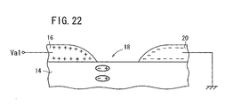
The electronic pulse generation device 10B according
to the second embodiment has substantially the same
structure as the electronic pulse generation device 10A
according to the first embodiment described above, but
differs from the electronic pulse generation device 10A in
that both the cathode electrode 16 and the anode electrode
20 are disposed on one surface of the emitter section 14,
with a slit 18 defined between the cathode electrode 16 and
the anode electrode 20, the emitter section 14 being partly
exposed through said slit 18.
-
As shown in FIG. 20, the electronic pulse generation
device 10C has electric field concentration points A, B.
The point A can also be defined as a triple point where the
cathode electrode 16, the emitter section 14, and a vacuum
are present at one point. The point B can also be defined
as a triple point where the anode electrode 20, the emitter
section 14, and a vacuum are present at one point.
-
The width d of the slit 18 between the cathode
electrode 16 and the anode electrode 20 is determined so
that polarization reversal occurs in the electric field E
represented by E= Vak/d (Vak is a voltage between the
cathode electrode 16 and the anode electrode 20). If the
width d of the slit 18 is small, the polarization reversal
occurs at a low voltage, and electrons are emitted at the
low voltage (e.g., less than 100V).
-
Dimensions of the cathode electrode 16 will be
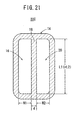
described with reference to FIG. 21. In FIG. 21, the
cathode electrode 16 has a width W1 of 2 mm, and a length
L1 of 5 mm. Preferably, the cathode electrode 16 has a
thickness of 20 µm or less, or more preferably 5 µm or
less.
-
Preferably, the anode electrode 20 is made by any of
the above thick-film forming processes. Preferably, the
anode electrode 20 has a thickness of 20 µm or less, or
more preferably 5 µm or less. In FIG. 21, the anode
electrode 20 has a width W2 of 2 mm, and a length L2 of 5
mm as with the cathode electrode 16.
-
In the embodiment of the present invention, the width
d of the slit 18 between the cathode electrode 16 and the
anode electrode 20 is 70 pm.
-
The principles of electron emission of the electronic
pulse generation device 10C will be described below with
reference to FIGS. 6, 20, and 22 through 23B. As shown in
FIG. 6, as with the first embodiment, in the third
embodiment, the drive voltage Va outputted from the pulse
generation source 22 has repeated steps each including a
period in which a first voltage Va1 is outputted
(preparatory period T1) and a period in which a second
voltage Va2 is outputted (electron emission period T2).
-
The preparatory period T1 is a period in which the
first voltage Va1 is applied between the cathode electrode
16 and the anode electrode 20 to polarize the emitter
section 14 in one direction, as shown in FIG. 22. The
first voltage Va1 may be a DC voltage, as shown in FIG. 6,
but may be a single pulse voltage or a succession of pulse
voltages. The preparatory period T1 should preferably be
longer than the electron emission period T2 for sufficient
polarization. For example, the preparatory period T1
should preferably be 100 µsec. or longer.
-
The electron emission period T2 is a period in which
the second voltage Va2 is applied between the cathode
electrode 16 and the anode electrode 20. When the second
voltage Va2 is applied between the cathode electrode 16 and
the anode electrode 20, as shown in FIG. 23B, the
polarization of at least a part of the emitter section 14
is reversed or changed. If the slit has a width d (see
FIG. 20) and a voltage Vak is applied between the cathode
electrode 16 and the anode electrode 20, then the
polarization of the emitter section 14 is reversed or
changed in an electric field E expressed by E = Vak/d,
which is applied to the material of the emitter section 14.
-
Because of the reversed or changed polarization, a
locally concentrated electric field is generated on the
cathode electrode 16 and the positive poles of dipole
moments in the vicinity thereof, emitting primary electrons
from the cathode electrode 16. As shown in FIG. 23B, the
primary electrons emitted from the cathode electrode 16
impinge upon the emitter section 14, causing the emitter
section 14 to emit secondary electrons.
-
In the present embodiment, the triple point A is
defined by the cathode electrode 16, the emitter section
14, and the vacuum. The primary electrons are emitted from
the cathode electrode 16 near the triple point A, and the
primary electrons thus emitted from the triple point A
impinge upon the emitter section 14, causing the emitter
section 14 to emit secondary electrons. If the thickness
of the cathode electrode 16 is very small (up to 10 nm),
then electrons are emitted from the interface between the
cathode electrode 16 and the emitter section 14.
-
Since the electrons are emitted according to the
principle as described above, the electron emission is
stably performed, and the number of emitted electrons would
reach 2 billion or more. Thus, the electronic pulse
generation device is advantageously used in the practical
applications. The number of emitted electrons is increased
substantially proportional to the amplitude Vin of the
drive voltage Va applied between the cathode electrode 16
and the anode electrode 20. Thus, the number of the
emitted electrons can be controlled easily.
-
Of the emitted secondary electrons, some are emitted
to the collector electrode 24 to excite the phosphor layer
28, which produces a fluorescent emission directed
outwardly. Other secondary electrons and the primary
electrons are emitted to the anode electrode 20.
-
In the electronic pulse generation device 10C
according to the third embodiment, polarization of the
emitter section 14 near the cathode electrode 16 is
reversed or changed differently from the electronic pulse
generation device 10A according to the first embodiment
(including modifications) and the electronic pulse
generation device 10B according to the second embodiment.
-
In the electronic pulse generation devices 10A, 10B
according to the first and second embodiments, only the
positive poles or the negative poles of the dipole moments
are oriented to the cathode electrode 16. Therefore, the
local electric field generated at the cathode electrode 16
is large. In contrast, in the electronic pulse generation
device 10C according to the third embodiment, the
electrodes are formed only on one principle surface of the
emitter section 14.
-
In the second and third embodiments, when polarization
of the emitter section 14 is reversed or changed, only the
positive poles are oriented to the cathode electrode 16
having the negative polarity. Thus, the primary electrons
are efficiently emitted from the cathode electrode 16.
-
In the electronic pulse generation devices 10A and 10B
according to the first and second embodiments, one
electronic pulse generation device 10A or 10B includes one
emitter section 14, and one cathode electrode 16 and one
anode electrode 20 formed on the emitter section 14.
Alternatively, a plurality of electronic pulse generation
devices 10(1), 10(2), 10(3) may be formed using one emitter
section 14 as shown in FIG. 24, for example.
-
Specifically, In the first example 100A shown in FIG.
24, a plurality of cathode electrodes 16a, 16b, 16c are
formed independently on a front surface of one emitter
section 14, and a plurality anode electrodes 20a, 20b, 20c
are formed on a back surface of the emitter section 14 to
form the plurality of electronic pulse generation devices
10(1), 10(2), 10(3). The anode electrodes 20a, 20b, 20c
are provided under the corresponding cathode electrodes
16a, 16b, 16c. The emitter section 14 is interposed
between the anode electrodes 20a, 20b, 20c and the cathode
electrodes 16a, 16b, 16c.
-
In a second example 100B shown in FIG. 25, a plurality
of cathode electrodes 16a, 16b, 16c are formed
independently on a front surface of one emitter section 14,
and one anode electrode 20 (common anode electrode) is
formed on a back surface of the emitter section 14 to form
a plurality of electronic pulse generation devices 10(1),
10(2), 10(3).
-
In a third example 100C shown in FIG. 26, one very
thin (up to 10nm) cathode electrode 16 (common cathode
electrode) is formed on a front surface of one emitter
section 14, and a plurality of anode electrodes 20a, 20b,
20c are formed independently on a back surface of the
emitter section 14 to form a plurality of electronic pulse
generation devices 10(1), 10(2), 10(3).
-
In a fourth example 100D shown in FIG. 27, a plurality
of anode electrodes 20a, 20b, 20c are formed independently
on a substrate 12, one emitter section 14 is formed to
cover these anode electrodes 20a, 20b, 20c, and a plurality
of cathode electrodes 16a, 16b, 16c are formed
independently on the emitter section 14 to form a plurality
of electronic pulse generation device 10(1), 10(2), 10(3).
The cathode electrodes 16a, 16b, 16c are provided above the
corresponding anode electrodes 20a, 20b, 20c. The emitter
section 14 is interposed between the anode electrodes 20a,
20b, 20c and the cathode electrodes 16a, 16b, 16c.
-
In a fifth example 100E shown in FIG. 28, one anode
electrode 20 is formed on a substrate 12, and one emitter
section 14 is formed to cover the anode electrode 20, and a
plurality of cathode electrodes 16a, 16b, 16c are formed
independently on the emitter section 14 to form a plurality
of electronic pulse generation devices 10(1), 10(2), 10(3).
-
In a sixth example 100F shown in FIG. 29, a plurality
of anode electrodes 20a, 20b, 20c are formed independently
on a substrate 12, one emitter section 14 is formed to
cover these anode electrodes 20a, 20b, 20c, and one very
thin cathode electrode 16 is formed on the emitter section
14 to form a plurality of electronic pulse generation
devices 10(1), 10(2), 10(3).
-
In the first through six examples 100A through 100F, a
plurality of electronic pulse generation devices 10(1),
10(2), 10(3) are formed using one emitter section 14. As
described later, the electronic pulse generation devices
10(1), 10(2), 10(3) are suitably used as pixels of a
display.
-
In the electronic
pulse generation devices 10A through
10C according to the first through third embodiments, the
collector electrode 24 is coated with a
phosphor layer 28
to for use as a pixel of a display as shown in FIG. 1. The
displays of the electronic
pulse generation devices 10A
through 10C offer the following advantages:
- (1) The displays can be thinner (the panel thickness =
several mm) than CRTs.
- (2) Since the displays emit natural light from the
phosphor layer 28, they can provide a wide angle of view
which is about 180° unlike LCDs (liquid crystal displays)
and LEDs (light-emitting diodes).
- (3) Since the displays employ a surface electron
source, they produce less image distortions than CRTs.
- (4) The displays can respond more quickly than LCDs,
and can display moving images free of after image with a
high-speed response on the order of µsec.
- (5) The displays consume an electric power of about
100 W in terms of a 40-inch size, and hence is
characterized by lower power consumption than CRTs, PDPs
(plasma displays), LCDs, and LEDs.
- (6) The displays have a wider operating temperature
range (- 40 to + 85°C) than PDPs and LCDs. LCDs have lower
response speeds at lower temperatures.
- (7) The displays can produce higher luminance than
conventional FED displays as the phosphor can be excited by
a large current output.
- (8) The displays can be driven at a lower voltage than
conventional FED displays because the drive voltage can be
controlled by the polarization reversing characteristics
(or polarization changing characteristics) and film
thickness of the piezoelectric material.
-
-
Because of the above various advantages, the displays
can be used in a variety of applications described below.
- (1) Since the displays can produce higher luminance
and consume lower electric power, they are optimum for use
as 30- through 60-inch displays for home use (television
and home theaters) and public use (waiting rooms, karaoke
rooms, etc.).
- (2) Inasmuch as the displays can produce higher
luminance, can provide large screen sizes, can display
full-color images, and can display high-definition images,
they are optimum for use as horizontally or vertically
long, specially shaped displays, displays in exhibitions,
and message boards for information guides.
- (3) Because the displays can provide a wider angle of
view due to higher luminance and fluorescent excitation,
and can be operated in a wider operating temperature range
due to vacuum modularization thereof, they are optimum for
use as displays on vehicles. Displays for use on vehicles
need to have a horizontally long 8-inch size whose
horizontal and vertical lengths have a ratio of 15 : 9
(pixel pitch = 0.14 mm), an operating temperature in the
range from - 30 to + 85°C, and a luminance level ranging
from 500 to 600 cd/m2 in an oblique direction.
-
-
Because of the above various advantages, the
electronic pulse generation devices can be used as a
variety of light sources described below.
- (1) Since the electronic pulse generation devices can
produce higher luminance and consume lower electric power,
they are optimum for use as projector light sources which
are required to have a luminance level of 200 lumens.
- (2) Because the electronic pulse generation devices
can easily provide a high-luminance two-dimensional array
light source, can be operated in a wide temperature range,
and have their light emission efficiency unchanged in
outdoor environments, they are promising as an alternative
to LEDs. For example, the electronic pulse generation
devices are optimum as an alternative to two-dimensional
array LED modules for traffic signal devices. At 25°C or
higher, LEDs have an allowable current lowered and produce
low luminance.
-