EP1421823B1 - Oberflächen-mikrobearbeitungsverfahren zur herstellung akustischer wandler - Google Patents
Oberflächen-mikrobearbeitungsverfahren zur herstellung akustischer wandler Download PDFInfo
- Publication number
- EP1421823B1 EP1421823B1 EP02733233A EP02733233A EP1421823B1 EP 1421823 B1 EP1421823 B1 EP 1421823B1 EP 02733233 A EP02733233 A EP 02733233A EP 02733233 A EP02733233 A EP 02733233A EP 1421823 B1 EP1421823 B1 EP 1421823B1
- Authority
- EP
- European Patent Office
- Prior art keywords
- layer
- membranes
- process according
- silicon
- semiconductor substrate
- Prior art date
- Legal status (The legal status is an assumption and is not a legal conclusion. Google has not performed a legal analysis and makes no representation as to the accuracy of the status listed.)
- Expired - Lifetime
Links
Images


Classifications
-
- H—ELECTRICITY
- H04—ELECTRIC COMMUNICATION TECHNIQUE
- H04R—LOUDSPEAKERS, MICROPHONES, GRAMOPHONE PICK-UPS OR LIKE ACOUSTIC ELECTROMECHANICAL TRANSDUCERS; ELECTRIC HEARING AIDS; PUBLIC ADDRESS SYSTEMS
- H04R19/00—Electrostatic transducers
Definitions
- This invention relates to a surface micromechanical process for manufacturing electro-acoustic transducers, particularly ultrasonic transducers, which enables an extremely high design flexibility to be achieved, in respect of the geometry and of the electrical and mechanical features of the device, as well as the maximum compatibility with the integration of control electronics directly on a substrate incorporating the transducers.
- this invention relates to an Electro-acoustic transducer manufactured by the above process and to an intermediate product of said process.
- the ultrasonic electrostatic capacitive transducers represent a suitable alternative to the piezoelectric transducers, since they are a solution of the problem of the 5 magnitudo order of mismatch with the air acoustical impedance.
- Such electrostatical capacitive transducers also designated as cMUT (Capacitive Micromachined Ultrasonic Transducers) are manufactured by planar surface micromanufacturing techniques on silicon, thereby offering the possibility to integrate the control electronics on the same chip.
- cMUT devices are specifically used for ecographic image acquisition, even if their application is not exclusively restricted to such field.
- these transducers enable to carry out multi-frequency ecographic scanning as well as the acquisition of three-dimensional images in real time, with a scarcely invasive examination, such as an acoustic examination.
- micromanufactured capacitive transducers were firstly realised in 1998 at the Stanford University, California, where a search team directed by Khuri Yakub has been working in this field for about ten years.
- the first process provides for a silicon substrate upon which a thermally grown sacrificial layer of silicon dioxide is realised.
- the thermal oxidation of the silicon broadly occurs at temperatures in the range of 900°C to 1200°C.
- a layer of silicon nitride is then deposited on said sacrificial layer by a low pressure chemical vapour deposition procedure or LPCVD procedure, which is generally carried out at temperatures in the range of 700°C to 900°C.
- the sacrificial layer is partially removed by an etching operation which should be carefully timed in order to control the membrane size.
- transducers comprising membranes of silicon nitride supported by portions of the silicon dioxide sacrificial layer that have not been removed by the etching operation.
- a second process provides for realising by a deposition procedure grooves of silicon nitride aimed at defining the borders of the silicon dioxide sacrificial layer areas, in order both to realise membranes of arbitrary shapes and to make the chemical etch timing less critical.
- transducers comprising membranes of silicon nitride rigidly supported by the silicon nitride grooves.
- the concerned silicon nitride should be deposited also in this second process by means of a LPCVD procedure at high temperature.
- a third process provides for a glass substrate upon which a polyamide sacrificial layer is realised.
- a layer of silicon nitride is deposited upon said sacrificial layer by means of a plasma enhanced chemical vapour deposition on PECVD procedure, which necessarily takes place at low temperatures, in the range of 200°C to 400°C, in order not to burn the polyamide.
- the sacrificial layer in partially removed by means of a carefully timed chemical etching operation aimed at controlling the membrane size.
- transducers comprising silicon nitride membranes supported by portions of the polyamide sacrificial layer not removed by said etching operation.
- the known prior art also includes document I. Ladabaum, X.
- U.S. Patent No. 5 870 351 discloses a process for manufacturing a large band ultrasonic transducer comprising a plurality of membranes of different geometric shapes electrically connected with one another.
- the disclosed manufacturing process is similar to the first process described in U.S. Patent No. 5 619 476 , with the possible variation in which a plastic material ring is provided for limitation of the sacrificial layer areas corresponding to the membranes.
- U.S. Patent No. 5 894 452 disclosing a process for manufacturing an ultrasonic transducer adapted to operate in submerged condition in a fluid.
- the manufacturing process as disclosed is again analogous to the first process described in U.S. Patent No. 5 619 476 , with addition of a further step aimed at sealing the vias by CVD deposition of a further silicon nitride layer.
- the size of the concerned vias appears to be particularly critic, in order to guarantee that no silicon nitride is introduced under the membranes during the sealing step.
- U.S. Patent No. 5 982 709 discloses a process for manufacturing an ultrasonic transducer wherein the membranes and their supports are formed during the same silicon nitride deposition and wherein the material deposited for sealing the vias is prevented from reaching the area underlying the membranes by defining the vias only in correspondence to tanks and to complex connection channels between the vias and the underlying areas of the membranes.
- This manufacturing process is analogous to the second process described in U.S. Patent No. 5 619 476 , with the possible variation of a polysilicon sacrificial layer, aimed at increasing the selectivity of the etching solution. Also in this process, the size of the vias appears to be particularly critic.
- PCT Application No. WO 00/72631 that disclosed an acoustic transducer and a process for manufacturing it similar to the previously mentioned ones, in which the lower metallisation is realised in the chambers formed just under the membranes.
- the described manufacturing process uses aluminium or silicon oxide deposited at low temperature as sacrificial materials.
- the materials utilised for making the electrodes are aluminium or copper or tungsten having low resistivity.
- the sacrificial layer, the membranes and the membrane supports are realised with only two different materials. This makes the selection of the process parameters and of the chemical etching solutions particularly critic for the obtainment of high selectivities, in order to control the geometry and the electrical and mechanical features of the process. Obviously, these critical aspects of the process make the latter particularly complex and expensive.
- the utilised materials and the processing temperatures cause an irregular planarity of the manufactured devices, thereby causing the establishment of significant parasitic capacitances in the transducers themselves, which, in turn, jeopardise their correct operation modes.
- the third process as proposed by the U.S. Patent No. 5 619 476 appears to be quite inefficient, due to the fact that polyamide is quite unsuitable as a support layer.
- this material has a quite low Young's modulus and therefore, a polyamide support for the concerned membranes would track the vibrations thereof, by absorbing them and generating beat effects.
- the intrinsic compression stress of the silicon nitride membranes deposited by a PECVD deposition procedure at low temperature appears to be extremely high, thereby further making the concerned membranes highly inefficient, while the membranes themselves should have a small intrinsic tensile stress.
- the residual mechanical stress level of the membranes of a transducer manufactured by the above discussed known processes is particularly high and hardly controllable, since it noticeably depends on the proportion between silicone (SiH 4 ) and ammonia (NH 3 ) and anyway it cannot be handled in arbitrary manner.
- Electro-acoustic transducers which enable to achieve in simple, inexpensive and reliable way a high design flexibility, in respect of the geometry as well as the electrical and mechanical features of the device, together within the maximum compatibility with the integration of control electronics directly on the same substrate incorporating the transducers.
- Another object of this invention is to provide a process of the above kind to maximise the planarity of manufactured transducers and to enable a dramatic reduction of the parasitic capacitances to be achieved in such devices.
- Such objects are realised by using silicon monoxide deposited at low temperature, as a structural support layer for the membranes.
- a further object of this inventions to provide a process of the above kind which enables a substantially arbitrary reduction to be obtained in the residual mechanical stresses in the membranes of the manufactured transducers.
- a still further object of this invention is to provide a process of the above kind which enables a dramatic reduction of the mechanical stress gradients in the membranes as caused by presence of vias therein.
- the silicon semiconductor substrate is a p-type doped silicon substrate having a resistivity no higher than 1 ⁇ .cm, preferably no higher than 2 ⁇ .cm.
- said silicon monoxide comprising structural layer has a thickness in the range of 100 nm to 1000 nm, preferably in the range of 400 nm to 600 nm, and said membranes of said resilient material can have a thickness no higher than 1000 nm, preferably no higher than 600 nm.
- the process according to this invention is innovative both in respect of the utilised materials and in respect of the implemented step set.
- the technologic process utilised a maximum temperature no higher than 600°C, thereby enabling an extremely high design flexibility to be obtained together with the direct integration of control electronics on the chip.
- the utilised techniques and novel material made it possible to realise a structurally integral device having all desired mechanical properties.
- the obtained device has been successfully tested both in respect of the electrical impedance measurement and in respect of the acoustic signal measurement in reception-transmission.
- the process according to this invention has been developed by successfully experimenting the pre-patterning technique for effectively controlling the geometry of the transducer components.
- the electrostatic cells were preliminarily shaped in order to achieve an optimum control of the dimensional and geometric features of the individual cells.
- Novel and not conventional materials never previously exploited in the micromanufacture field have been utilised in this process.
- Particular relevance is to be attributed to utilisation of low temperature evaporate silicon monoxide as a structural layer to form the side supports of the membranes, also designated hereinafter as "rails".
- the low temperature deposition technique it is perfectly compatible with the photoresist as needed for the subsequent lifting removal or simply lift off operation, as well as with the organic material utilised as sacrificial layer.
- the lift off technique offers simplicity and unexpensiveness advantages in the process exploitation.
- the polyamide utilised as sacrificial layer enables an exceptional chemical etching selectivity to be obtained in respect of the material by which the transducer is made, thereby allowing to maintain the characteristic properties of the structural layers.
- the mechanical properties of the silicon nitride film grown by a PECVD technique appear to be easier to be controlled.
- a particular technique has been established to remove the sacrificial layer in order not to cause the adhesion of the structural layer to the substrate (stiction).
- the characteristics of the process according to this invention are the realisation of a pre-patterning procedures for the cavities, the utilisation of silicon monoxide to form the rails, the utilisation of a PECVD reactor for deposition of the layer that forms the membranes and the utilisation of chromium or of a polymer, namely a polyamide, as a sacrificial layer, which enable to planarise the surface upon which the silicon nitride will be subsequently deposited.
- the pre-patterning step is very important because if offers a valid stoppage to the chemical attack, or etch stop, on releasing the membranes and the chromium or the polymer are easily workable by the usual micromanufacturing techniques on silicon.
- the high process versatility is made possible in view of the fact the chemical etch utilised for removal of the chromium or the polymer, offers a 100% selectivity in respect of the utilised materials, such as the silicon nitride, the silicon monoxide and the silicon itself. By this procedure, the materials by which the transducer will be effectively made are in no way deteriorated, thereby maintaining all their quality levels in respect of strength and density.
- the apertures or vias for etching the sacrificial layer are realised by means of a lithographic process and are optimised so as to be subsequently closed in the final stage again by means of a lithographic process.
- a further result achieved by this invention in that a capacitive transducer cMUT of a new kind has been realised, comprising an array of suitably parallel to one another connected, electrostatic cells, having an interelectrode spacing noticeably reduced with respect to the cMUT transducers of the previous generations.
- This result has been made possible by realising the lower metallisation of the device on the upper side of the starting substrate just under the cavities and the membranes, thereby enabling the distances between lower and upper electrodes to be reduced by an amount substantially equal to the substrate thickness.
- a novel technologic process has been designed for manufacturing a transducer adapted to operate in more efficient manner and at higher frequencies as well as with reduced parasitic capacitances in comparison to previously realised devices.
- 340 devices corresponding to twelve different geometries are manufactured on a single wafer.
- the realisation of a so large number of devices per wafer is possible in view of the fact that each device has a surface area of only 3 mm 2 .
- each individual electrostatic cell has been selected since this shape optimises the characteristics of the generated acoustic ultrasonic filed to the best.
- the process according to this invention starts from a silicon wafer grown according to the Czochralski methods, or CZ silicon, p-type doped with boron (density: 10 17 cm -3 ), having a resistivity of about 0,1 ⁇ . cm and with crystallographic orientation ⁇ 100>.
- the side of the wafer on which the process is carried out is lapped.
- Table 1 Type Rail minimum dimension Number of Membranes per device Membrane diameter
- the first step to be carried out is the application of a polyamide layer which will subsequently suitably etched in order to realise the layout that should receive the support rails of the structural layer.
- the polyamide layer forms the sacrificial layer and its thickness identifies the distance by which the membrane will be spaced from the substrate upon being released therefrom.
- the polyamide represents the end treatment stage of a monomer solution that is applied to the wafer by means of a high speed centrifugation technique or spinning. Two successive thermal treatments are subsequently carried out in order to promote the polymerisation reaction which results into a product designated as polyamide.
- the thickness of the layer depends on the rotation speed and decreases after the polymerisation process is completed.
- the polyamide utilised herein (N-methyl-2-pyrrolidone) is a polymer manufactured by Olin Microelectronic Materials having trade name Probimide 112A selfpriming cat 851089.
- the preliminary treatment of the wafer comprises a cleaning step to remove the atmospheric dust, performed by putting the wafer under a jet of deionised running water and then drying it by a jet of nitrogen. More adherent particles are removed by immersing the sample into an acetone bath in a tank run through by ultrasonic waves, in order to exploit the cavitation effect.
- a cleaning operation particularly aimed at removal of organic residuals and fat acids can be carried out by immersion into a bath formed by a solution comprising 70% sulphuric acid (H 2 SO 4 ) and 30% hydrogen peroxide (H 2 O 2 ).
- a last dry cleaning step can be carried out by utilising oxygen plasma.
- All water residuals, which could jeopardise the adhesion of the polymer to the surface, could be removed by means of a drying step carried out by heating the wafer in a furnace at 150°C for 20 minutes.
- the wafer in then arranged on the circular plate which the spinner is provided with, about 3 ml polyamide are put at the central area of the plate and this plate is then rotated, initially at low speed, until the polyamide reaches the edge of the wafer, then speed is increased up to 4000 rpm during a total time of 120 seconds.
- the so prepared wafer is then treated in a furnace at a temperature of 120°C for 30 minutes, in order to evaporate the solvents having the monomers dissolved therein.
- the last preparation stage of the layer to be subsequently utilised as a sacrificial layer consists in the polymerisation process.
- the sample is arranged upon a quartz support in horizontal position within a metal wall furnace, immersed in a nitrogen flow.
- the thickness measured after the polymerisation stage is about 890 nm, which is higher than the 500 nm limit as required by the specifications of the preferred embodiment of the process.
- a thinning stage should subsequently be carried out by means of a dry etching operation in RIE with a CF 4 flow rate of 12.6 sccm (standard cubic centimetres per minute), an 0 2 flow rate of 60 sccm, under a pressure of 5.3 Pa, a power of 100 W and a via voltage of 200 V: the removal rate is found to be 2.5 nm/s.
- the lower electrode of the reactor should be protected by means of a large silicon wafer, because it enables a higher etching spatial uniformity to be achieved.
- the etching time is of about 150 s.
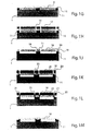
- the pre-patterning operations consist in etching the polyamide layer 2 in order to form islands corresponding to the membranes that form the sacrificial layer.
- the etching procedure is carried out as a dry etching operation in a suitable plasma, by utilising an optical resist as a masking layer.
- a positive photolithographic process is utilised in order to define the areas to be etched away in the polyamide film.
- the mask utilised in the optical lithographic process is realised by means of an electronic lithographic process. It is possible to realise on the same mask six different device typologies in respect of the via arrangement, as it is shown in Figures 2A-2F .
- Figure 2A The typology of Figure 2A is designed to realise a single via for each membrane 3 at its centre area and it is almost designed to manufacture a process control device.
- the other typologies provide for realising the vias outside the circular membrane 3, in order to disturb the circular geometry to the minimum possible extent.
- the vias are positioned within the outwardly protruding lunettes 4.
- the vias should be arranged in order to be superimposed on the thin channels 5 protruding from membrane 3.
- Figure 2C provides for arranging the vias 6 completely outwardly of membrane 3 and the chemical etch of the sacrificial layer reaches the area corresponding to membrane 3, namely the air gap, through the connection channels 7.
- This geometry in addition to being scarcely perturbative enables optimum results to be obtained particularly at the stage in which the vias are to be closed, since the filling of the vias is not critic to membrane vibration, because it is sufficiently spaced apart and not tangent as in the other typologies.
- a frame for separating the 340 transducers has been realised in order to aid performing the final cutting operations.
- the frame layout is shown in Figure 3 , where the devices with membranes of 40 ⁇ m diameter have been realised in the upper half section, while the devices with membranes of 50 ⁇ m diameter have been realised in the layer half section.
- polyamide islands having the shapes illustrated in Figures 2A-2F are obtained.
- polyamide islands 8 can be observed, such islands being protected by optical resist masks 9, between which the layout 10 that will be filled by rails of silicon monoxide has been etched.
- the etching operation of the polyamide takes place in RIE in order to obtain a more vertical removal with respect to the wet etching operations.
- the etching operation is carried out with a formulation as already defined in connection with the thinning stage of the polyamide.
- the etching time for removing 480 nm of polyamide is of about 156 s and it should be carefully controlled, because this formulation entails a silicon removal and, therefore, the risk to etch the substrate is run.
- the thickness control is effected by means of a profilometer.
- the optical resist masks 9 are not removed.
- the rails are realised by thermally evaporated silicon oxide.
- the choice of this material is suggested by the fact that, since a material is to be deposited upon the optical resist in view of the subsequent lift off step, it is necessary to carry out a low temperature process in view of the scarce heat resistance of such material. No particular treatment of the wafer is carried out before evaporation of the silicon oxide, besides the usual removal operation of the dust particles in deionised water and in nitrogen flow.
- the thickness of the evaporated silicon oxide depends on the polyamide thickness existing on the sample, because both the oxide and the polyamide are to be levelled in order to obtain as much planar membranes as possible.
- the deposited thickness is equal to 500 nm.
- the subsequent step provides for removing the silicon monoxide areas 12.
- the sample is immersed in acetone in order to dissolve the resist masks 9 by removing then the superimposed monoxide areas 12.
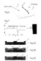
- Figure 4 illustrates the three-dimensional reconstruction of the monoxide-polyamide interface profile based upon a surface scan obtained by means of an atomic force microscope or AFM.
- Figure 5 illustrates the cross-section of the same profile and the measurement of the differences in height existing between the polyamide island 8, the monoxide rail 11 and monoxide residual 13.
- the immersion is performed before carrying out the lift off operation by means of an acetone bath, in order that the resist layer and the silicon oxide protect the underlying polyamide.
- This measure further improves the resist dissolution rate and accuracy in the subsequent acetone bath, because the vertical sides will be more exposed to the etching solution.
- the depth of the groove is not amenable to raise problems because the 500 nanometres of silicon nitride to be deposited thereon will be sufficient to fill it up.
- a planarisation step is carried out by means of a chemical - mechanical polishing operation, by utilising a silica particle solution in alkaline environment, by rubbing the wafer against a hard surface, preferably a glass surface. The surface turns out to be completely planarised at the end of the polishing procedure, without formation of grooves at the edges of the rails 11 ( Figure 8C ).
- layer 15, by which said membranes are formed is realised by silicon nitride deposited by utilising a PECVD reactor.
- the thickness of the deposited film is of about 500 nm.
- a good adhesion is achieved between the silicon nitride and the monoxide.
- a preliminary cleaning operation is carried out in acetone for 300 s followed by rinsing in deionised water.
- a PECVD procedure In comparison to films grown by a LPCVD procedure, a PECVD procedure enables films to be deposited at low temperatures, lower than 400°C, and with mechanical characteristics variable within an extended range.
- the deposition of films of high quality at low temperatures allows to utilise, for the sacrificial layer, materials that can be removed very rapidly and with very high selectivity in respect of silicon nitride, such as polyamide or optical resist.
- the control of the growing parameters of the silicon nitride films is essential for the obtainment of efficient membranes.
- Figure 9 shows a diagram of the compression stress behaviour as a function of the silane/nitrogen ratio according to the measurements affected.
- the mechanical stress in the membranes can be modified by means of heat treatments carried out after the film deposition. Heating the silicon nitride to temperatures higher than 500°C causes thickening of the film due to hydrogen desorption with formation of linkages between silicon and nitrogen. The reduction of the linkages Si-H (about 2100 cm -1 ) clearly appears from the absorption spectrum of Figure 10 . This spectrum is obtained by infrared spectroscopy or FTI, and it results from subtraction of the absorption of a silicon sample with 400 nm nitride and of the absorption of a clean silicon sample. The noise encountered in connection with wave numbers higher than 2200 cm -1 is due to variations in air absorption between the acquisitions.
- the holes through which the etching operation of the silicon nitride is carried out by means of a RIE etching procedure, aimed at realising the vias 16, are defined by a subsequent lithographic operation.
- the etching operation is carried out with a CHF 3 flow rate of 50 sccm, an O 2 flow rate of 8 sccm, a pressure of 7.1 Pa, a power of 180W and a bias voltage of 260 V: the removal rate of the silicon nitride 15 turns out to be 0.67 nm/s, while the removal rate of the optical resist 17 is of 0.5 nm/s.
- the etching time to realise a through hole in a standard membrane of 500 nm is of about 600 s, but aiming at assuring that said vias 16 reach the sacrificial layer 8, such duration is extended to 900 s, without causing any damage, also keeping in mind that said sacrificial layer will be eventually removed.
- the silicon nitride membranes 18 are suspended on an air gap 19 of 500 nm and are substained by rails 11 of silicon monoxide.
- the chemical etching step on the polyamide is carried out preferably by immersion in a 7:3 solution of sulphuric acid (H 2 SO 4 ) and hydrogen peroxide (H 2 O 2 ) that strongly attacks any compound, particularly the polyamide, by means of a highly exothermal reaction, rapidly reaching 353K.
- H 2 SO 4 sulphuric acid
- H 2 O 2 hydrogen peroxide
- the complete removal of the sacrificial layer is carried out in just 2400 s time and the 100 % selectivity assures a perfect integrity of the silicon oxide and silicon nitride films.
- FIG. 11 shows the three-dimensional reconstruction effected by said AFM for a membrane according to typology of Figure 2C , subjected to a compression stress after release, which makes it cambered upwardly.
- Figure 12 shows the cross-section of the membrane of Figure 11 : the camber of the membrane is of about 1 nm which, when compared to 40nm diameter of the membrane, does not appear to be so relevant.
- a tensile stress appears to be preferable with respect to a compression stress.
- the stress is gradually relieved by means of thermal treatments in which the sample is heated to a temperature in the range of 490 °C to 530°C, preferably a temperature equal to 510°C.
- Figure 13 shows the variation of the membrane profile achieved by subjecting the concerned device to two thermal annealing treatments, each extended to a 5 hour duration.
- the first annealing treatment is carried out before the removal of the polyamide sacrificial layer, thereby reducing the compression stress and also making it not destructive during the release step of the membranes.
- the duration of the first thermal treatment can be such as to completely consume the polyamide material, thereby making the removal to be effected by chemical etching redundant. Further thermal treatments can be carried out in order to further reduce the intrinsic compression stress and to introduce an intrinsic tension stress into membranes.
- the annealing treatments allow to achieve a very high design flexibility, also in terms of geometry and dimensions of the membranes.
- the vias can be closed by means of a silicon monoxide deposition, having a thickness equal to the thickness of the air gap 19, and of an optical lithography operation. Lastly, a metallisation of both sides of the wafer is carried out.
- the closure of the vias takes place as a column filling thereof by utilising silicon monoxide that forms the stoppers 22.
- the thickness of the monoxide layer 20 as deposited ought to be sufficient to form stoppers 22 reaching the underlying nitride 18.
- the deposition technique is a low temperature evaporation based upon heating by Joule's effect a crucible containing silicon monoxide grains.
- the monoxide layer 20 deposited on membranes 18 should be removed because otherwise it would not allow a correct operation of the transducer.
- the removal is carried out by means of an optical lithographic operation with subsequent etching operation in RIE.
- the optical lithographic procedure is needed because it is necessary to create a mask layer 21 consisting of an optical resist, suitably shaped in order to protect said stoppers 22 from the etching agent acting on the silicon monoxide, leaving the monoxide 20 superimposed to the membrane 18 exposed.
- the thickness of the resist is 1.5 nm.
- Etching of the silicon monoxide is carried out in RIE according to the formulation already discussed in respect of the etching operation performed on silicon nitride for realising the vias.
- the etching time is of about 875 seconds.
- the utilised formulation slowly removes also said optical resist, but this does not raise any problem, because it has a endurance well beyond the duration of the etching operation.
- the utilised formulation is not selective in respect of the underlying silicon nitride, so that, during the etching operation, it is necessary to control the oxide removal status, in order to stop the procedure as soon as it is finished.
- the residual resist is removed by an oxygen plasma in RIE, under an O 2 flow rate equal to 67 sccm, a pressure equal to 5,3 Pa, a power equal to 100 W and a bias voltage equal to 200 V.
- the sample can be immersed in acetone for a few minutes and then rinsed in deionised water.
- the product shown in Figure 1M is obtained.
- the back surface of the wafer is metallised by deposition of an aluminium film 23 of 150 nm thickness.
- the surface to be metallised is of not-lapped silicon. Such surface should be cleaned and not oxidised, in order to guarantee a good adhesion of the film as well as a good ohmic contact.
- the wafer is heated to 650K for 1800 seconds in order to improve the ohmic contact, in a steel furnace, under a nitrogen flow rate of 30 sccm.
- the metallisation pattern is realised by means of an optical lithographic process, with utilisation of a mask realised by an electronic lithographic process.
- the aluminium film applied for metallisation of the membranes is deposited by sputtering.
- the metal layer patterning operation is carried out by means of a further optical lithographic process, with utilisation of a mask realised by means of an electronic lithographic process, thereby obtaining the metallisation areas 24 of the membranes 18.
- the chromium layer as deposited is suitably patterned by means of an optical lithographic process, in order to obtain a structure exclusively entailing the metallisation of a restricted area corresponding to the cavities or hollow chambers and to the membranes.
- the upper metallisation is realised by deposition of an aluminium layer, rather than chromium, in view of the fact that the latter would grow with a highly tensile mechanical stress, which sometimes could be destructive for the membranes.
- the aluminium film is subsequently treated in order to define the metallised areas on the membranes and their interconnections, positioned with a complementary configuration with respect to the interconnections of the lower metallisation, in order to limit the incidence of parasitic capacitances.
- Another noticeable improvement is related to utilisation of chromium as sacrificial material in substitution for the most common silicon compounds.
- the chemical etching operation utilised for its removal has a selectivity of 100% in respect of the other materials utilised therein, such as the silicon nitride, the silicon monoxide and the silicon itself, thereby assuring a perfect control of the active region of the transducer.
- the materials by which the device will be effectively formed are in no way deteriorated, thereby maintaining all their performances in respect of resistance and density.
- the pre-patterning technique is exploited by defining, by means of a photolithographic procedure, the sacrificial islands before deposition of the membranes, in order to guarantee a micrometric definition of the device geometry.
- the hollow chambers or cavities upon which the membranes are suspended effectively represent the active regions of the transducer. Their geometry and dimension represent the main factors by which the performances of the device are characterised.
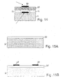
- Figure 14 shows a microcell of the transducer manufactured by means of the third embodiment of the manufacturing process according to this invention.
- the lower metallisation 25 is directly realised on the upper surface of the wafer, just under the membranes 18 and the corresponding cavities, thereby reducing the distance between stationary lower electrodes and the mobile upper electrodes by a thickness substantially equal to the thickness of substrate 1, equal to about 380 nm.
- the third embodiment of the manufacturing process according to the invention utilises 3" p-type doped silicon wafers, having a resistivity of about 0.1 ⁇ .cm with crystallographic orientation ⁇ 100>.
- a number of 340 devices are micromachined on a single wafer, each of which is characterised by 1512 membranes. A so high number of devices is made possible by the small area engaged by each of them equal to 3 mm 2 .
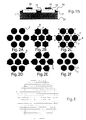
- Each membrane has a circular type shape realised by referring to polygons of 16 sides. Such a geometry perfectly matches the characteristics of the acoustic field generated.
- the individual membranes appear to be arranged according to a configuration of a matricial type with a minimum distance of 10 nm from one another.
- One half of the devices realised on the wafer are formed by membranes each having a diameter of 40 nm, while the devices of the other half are formed by membranes having a greater diameter equal to 50 nm.
- an insulating layer 26 of thermal silicon dioxide SiO 2 is deposited to isolate the starting silicon substrate 1 from the lower metallisation.
- the process provides for realising the lower electrodes 25.
- the lower metallisation is realised by depositing a uniform chromium layer by evaporation.
- the chromium film is subsequently patterned by means of an electronic lithographic process aimed at imparting a particular geometric shape to the lower metallisation.
- the need to reduce the parasitic capacitances of the transducer resulted into metallisation of the membranes 18 only so that the connections between the electrodes 25 are realised by means of suitable conductive paths realised in positions corresponding to the rails 11 and the thickness of which is not higher than 4 nm.
- the dimensions of the electrodes 25 are selected to optimise the performances of the transducer.
- each membrane 18 are exclusively realised in the central portion of each membrane 18 so as to increase the ratio between the capacitance modulation and the static capacitance of the device. Due to this reason, the process realises electrodes 25 utilising only 60% of a surface corresponding to the surface of the membranes 18 and with a small thickness if compared to the thickness of the membranes 18. When membranes 18 having diameters of 40 ⁇ m and 50 ⁇ m are realised, the obtained electrodes 25 have diameters of 24 ⁇ m and 30 ⁇ m, respectively.
- Connection pads are utilised to allow the realisation of an electric contact between the electrodes 25 and the external circuit.
- the pattern of the lower electrodes 25 and of their related interconnections is protected by means of a film 27 of silicon nitride SiN grown by means of a PECVD technique.
- a film 28 of chromium is deposited by means of an evaporation technique as a sacrificial material.
- pre-patterning of sacrificial islands 8' is carried out by means of an optical lithographic process, by utilising a suitable mask realised by means of an electronic lithographic process.
- a subsequent wet etching operation is carried out on said chromium in order to define the regions forming said island 8'.
- the chromium layer exclusively remains unaltered in regions corresponding to the area by which the cavities (air gap) of the transducer will be characterised.
- the above said layer 28 defines the thickness of the cavity in the transducer and, therefore, it is a critical variable in designing the performances of the transducers.
- the resist (not shown) applied upon the islands 8', which is not exposed during the lithographic process, is not removed in order to permit execution of the subsequent step of the process.
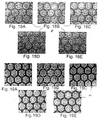
- Figure 18A, 18B, 18C and 18E show the optical microscope images of the chromium sacrificial islands 8' before the monoxide rails 11 are formed, respectively corresponding to the five geometric shapes of the etching holes shown in Figures 2B, 2C, 2D, 2E and 2F .
- a layer of silicon monoxide SiO is deposited by means of an evaporation operation based upon the Joule's effect, in order to realise a planar type structure and to create rails 11 aimed at supporting the membranes 18.
- the excess monoxide grown upon the islands 8' is removed by means of a lift off process, by dissolving the resist not removed by the previous step, by acetone and ultrasounds.
- the thickness of the deposited monoxide is equal to the thickness of the sacrificial islands 8' in order to obtain rails 11 having the same height as the cavities. This enables a subsequent structural layer of the membranes 18 to be deposited upon a planar type surface, thereby assuring a uniform stress distribution in the membranes and avoiding possible breakage points for the membranes themselves.
- Figures 19A, 19B, 19C, 19D and 19E show the optical microscope images of the chromium sacrificial islands 8' after the monoxide rails 11 have been created, respectively corresponding to the five geometric shapes of the etching holes shown in Figures 2B, 2C, 2D, 2E and 2F .
- the realisation of the membranes 18 is carried out by depositing a layer 15 of silicon nitride SiN x by exploiting a PECVD technique.
- the residual stress of the nitride film 15 can be controlled by varying the plasma frequency, the substrate 1 temperature and the nitrogen and silicon relative concentrations during the deposition process.
- the intrinsic stress in the silicon nitride membrane 18 has been designed so as to have a scarce tensile character by controlling the radiofrequency power in the PECVD process.
- the thickness of the film 15 can be controlled in the PECVD process, as well.
- the stress under which the film 15 is grown represents an essentially important factor in view of the fact that, as previously discussed, the resonance frequency of the membrane 18 depends thereon.
- a thermal annealing step of the sample is then carried out in order to reduce the compression stress in the membranes 18, which would cause a subsequent camber effect as well as their breakage after releasing thereof, with conversion of the compressive stress into a weakly tensile stress.
- submicrometric apertures 16 are defined, by means of an optical lithographic process, on the membrane 18 area, in order to enable chromium to be subsequently removed from the underlying sacrificial islands 8'.
- the above mentioned apertures 16 are provided in perimetral positions on each individual membrane according to five different typologies as shown in Figures 2B-2F , which assure an efficient etching of said sacrificial islands 8' as well as an excellent mechanical stability of the structure.
- a mask with a pattern of holes 16 having a design diameter of 4 nm is realised by means of an electronic beam lithographic process.
- the dimensions of the vias 16 should be small, in order to enable the holes to be closed and the cavities be sealed, but, on the other hand, they should be sufficiently large as to enable the underlying sacrificial layer to be removed.
- the realisation of said silicon nitride vias 16 is carried out on the silicon by means of a dry etching operation with a reactive ion etching (RtE) technique.
- RtE reactive ion etching
- the product at this point consists of a matrix of silicon nitride membranes 18 suspended on silicon monoxide supports 11.
- the vias 16 are closed by column filling them with the same material by which the rails 11 are formed.
- the thickness of the monoxide layer 20 as deposited should be sufficient to form stoppers 22 extended up to reaching the overlying silicon nitride layer 18.
- the removal of the monoxide layer 20 deposited on said membranes 18 is carried out by means of an optical lithographic process and a dry etching operation in RIE, thereby obtaining the product shown in Figure 15L .
- the optical lithographic step allows to realise a masking layer of optical resist so shaped as to protect the above said stoppers 22 in respect of the etching step carried out on the silicon monoxide and to leave the monoxide overlying the membranes 18 uncovered, in similar way as shown in Figure 1L .
- said etchant holes 16 be closed, not only in order to enable the concerned transducers to be utilised in immersed condition, but also to protect the cavities from possible contaminations that could modify the vibration properties of said membranes 18, with resulting alteration of the performances of the concerned transducer.
- a thin film of silicon nitride SiN is preferably grown subsequently by means of PECVD technique, which enables hermetic sealing of said vias 16, without significantly modifying the vertical dimension of the transducer.
- the subsequent process step is aimed at realising the upper metallisation.
- a conductive layer of aluminium is deposited by a sputtering operation.
- a subsequent deposition of a thin layer of titanium is then carried out also by sputtering.
- the pattern of the upper electrodes 24 and of the related interconnections is realised by means of an optical lithographic process, under utilisation of a mask realised by means of an electronic lithographic process. Aiming at reducing the parasitic capacitances of the transducer, only said membranes 18 are metallised. Corresponding to rails 11 only connections between electrodes 24 are provided in complementary positions with respect to the connection paths of the electrodes 25 of the lower metallisation, in order to avoid useless overlaps and to reduce any possibly existing parasitic capacitances. The contact to the external circuitry occurs by means of a suitable pad.
- the titanium layer in the exposed regions of the optical resist is then removed by means of a dry etching operation in RIE.
- the underlying exposed aluminium layer is removed by a wet etching operation in a suitable etchant solution, thereby obtaining the product shown in Figure 15M .
- the pads corresponding to the lower metallisation are opened by means of a lithographic process with related mask and by means of a dry etching operation in RIE aimed at removing the structure silicon nitride SiN x and the silicon monoxide layers.
- the wafer is then covered by a thin protection layer 28 of silicon nitride SiN x grown by means of a PECVD technique, utilised for protecting the upper metallisation and to assure hermetic sealing of the cavities.
- the pads are opened in order to enable the realisation of the contacts to the measurement external circuitry, by means of an optical lithographic process, with utilisation of a mask realised by means of an electronic lithographic process and a dry etching operation in RIE, for removal of the protection silicon nitride SiN x corresponding to the lower and upper pads.
- Figure 16A shows a first configuration as utilised for the lower metallisation clearly evidencing pad 29 for connection to the external circuitry.
- Figure 16B shows an enlarged portion of the configuration of Figure 16A .
- Figure 17A shows a second configuration as utilised for the lower metallisation
- Figure 17B shows an enlarged portion thereof.
- Figures 20A, 20B, 20C and 20D show optical microscope images of the finished device, clearly evidencing the membranes 18, the rails 11, the etchant vias 16 and the lower electrodes 25 and upper electrodes 24.
- Figure 21 is an AFM view of a membrane 18 before the thermal annealing step
- Figure 22 is an AFM of the same membrane 18 after the thermal annealing step.
Landscapes
- Physics & Mathematics (AREA)
- Engineering & Computer Science (AREA)
- Acoustics & Sound (AREA)
- Signal Processing (AREA)
- Transducers For Ultrasonic Waves (AREA)
- Micromachines (AREA)
- Pressure Sensors (AREA)
- Measuring Volume Flow (AREA)
- Piezo-Electric Transducers For Audible Bands (AREA)
Claims (20)
- Oberflächen-Mikrobearbeitungsverfahren zur Herstellung von elektro-akustischen Wandlern, insbesondere UltraschallWandlern, wobei die Wandler ein Silizium-Halbleitersubstrat (1) umfassen, wobei auf einer oberen Oberfläche von diesem eine oder mehrere Membranen (18) aus nachgiebigen Materialien durch eine Strukturschicht (11) aus isolierendem Material getragen sind, das fest mit dem Halbleitersubstrat (1) verbunden ist, wobei das nachgiebige Material ein Young'sches Modul aufweist, das nicht geringer als 50 GPa ist, wobei die Membranen (18) metallisiert sind, wobei die Wandler eine oder mehrere untere Elektroden (23, 25) enthalten, die fest mit dem Halbleitersubstrat (1) verbunden sind, wobei das Verfahren die folgenden Schritte umfasst:A. Bereitstellung eines Silizium-Halbleitersubstrats (1),B. Realisierung eines Zwischenprodukts, umfassend:- eine Opferschicht (8, 8') aus Opfermaterial, und- eine Strukturschicht (11) aus isolierendem Material,
das fest mit einer oberen Oberfläche des Silizium-Halbleitersubstrats (11) verbunden ist, wobei die Oberflächen der Opferschicht (8, 8') und der Strukturschicht (11), nicht in Kontakt mit dem Substrat (1), im Wesentlichen koplanar sind,C. Abscheidung einer Schicht (15) des nachgiebigen Materials auf der Opferschicht (8, 8') und auf der Strukturschicht (11), undD. Realisierung der Membranen (18) aus dem nachgiebigen Material durch Entfernen der Opferschicht (8, 8') von dem Produkt, das gemäß Schritt C erhalten wurde,wobei die Strukturschicht (11) Siliziummonoxid enthält und das Opfermaterial sich von dem isolierenden Material der Strukturschicht (11) unterscheidet,
wobei das Verfahren dadurch gekennzeichnet ist, dass das Opfermaterial (8) ein organisches Polymer umfasst, das aus der Gruppe ausgewählt ist, die Polyamide und Polymere von Benzocyclobuten und seinen Derivaten umfasst, wobei das organische Polymer vorzugsweise Polyamide, besonders bevorzugt N-Methyl-2-Pyrrolidon umfasst. - Verfahren gemäß Anspruch 1, dadurch gekennzeichnet, dass sämtliche der Schritte des Verfahrens bei Temperaturen ausgeführt werden, die nicht höher als 600°C, vorzugsweise nicht höher als 530°C sind.
- Verfahren gemäß einem der vorhergehenden Ansprüche, dadurch gekennzeichnet, dass das nachgiebige Material einen Wert des Young'schen Moduls aufweist, der nicht kleiner als 100 GPa ist, wobei das nachgiebige Material vorzugsweise entweder Siliziumnitrid oder kristallines Silizium umfasst.
- Verfahren gemäß einem der vorhergehenden Ansprüche, dadurch gekennzeichnet, dass das Opfermaterial (8') Chrom umfasst.
- Verfahren gemäß einem der vorhergehenden Ansprüche, dadurch gekennzeichnet, dass Schritt D die folgenden, aufeinander folgend geordneten Unter-Schritte umfasst:D.1 Realisierung von einer oder mehreren Aperturen oder Lücken (16) auf der Schicht (15) aus nachgiebigem Material, angepasst um einen Zugriff zu der Opferschicht (8) von außen zu ermöglichen undD.2 thermische Behandlung durch Ausheizen des Produkts, das gemäß Schritt C erhalten wurde, wobei das Produkt, das gemäß Schritt C erhalten wurde, vorzugsweise auf eine Temperatur im Bereich von 490°C bis 530°C erwärmt wird.
- Verfahren gemäß Anspruch 5, dadurch gekennzeichnet, dass Schritt D ferner indifferent vor oder nach dem Unter-Schritt D.1 oder D.2 den folgenden Unter-Schritt umfasst: D.3 chemisches Ätzen der Opferschicht.
- Verfahren gemäß Anspruch 6, dadurch gekennzeichnet, dass, wenn der Unter-Schritt D.3 auf den Unter-Schritt D.2 folgt, der Schritt D ferner nach dem Unter-Schritt D.3 den folgenden Unter-Schritt umfasst:D.4 thermische Behandlung durch Ausheizen des Produkts, das gemäß Schritt C erhalten wurde, wobei das Produkt, das gemäß Schritt C erhalten wurde, vorzugsweise auf eine Temperatur im Bereich von 490°C bis 530°C geheizt wird.
- Verfahren gemäß einem der Ansprüche 5 bis 7, dadurch gekennzeichnet, dass die Gesamtdauer der Ausheiz-Operation für das Produkt, das gemäß Schritt C erhalten wurde, angepasst ist, um die intrinsische Kompressionsspannung der Membranen (18) nicht höher als 10 MPa herzustellen, wobei die Gesamtdauer der Ausheiz-Operation für das Produkt, das gemäß Schritt C erhalten wurde, vorzugsweise angepasst ist, um die intrinsische Zugspannung der Membranen (18) in dem Bereich von 10 MPa bis 50 MPa umfasst herzustellen.
- Verfahren gemäß einem der vorhergehenden Ansprüche, dadurch gekennzeichnet, dass die Lücken (16) extern zu den Orten der Membranen (18) und mit einem Abstand davon positioniert sind, angepasst, um im Wesentlichen vernachlässigbare Spannungsgradienten einzuführen, wobei die Opferschicht (8) Kanäle (7) umfasst, um die Positionen der Lücken (16) zu den Orten der Membranen (18) zu verbinden.
- Verfahren gemäß Anspruch 4, dadurch gekennzeichnet, dass Schritt B die folgenden, aufeinanderfolgend geordneten Unter-Schritte umfasst:B.1 Abscheidung einer Chrom umfassenden Schicht (28) auf der oberen Oberfläche des Halbleitersubstrats(1),B.2 Definition von Konfigurationen oder Mustern in der Chrom umfassenden Schicht (28), indem Aussparungen in der Chrom umfassenden Schicht (28) erzeugt werden, vorzugsweise mittels eines optisch-lithografischen Verfahrens, das unter Verwendung einer Maskierungsschicht aus fotolithografisch gemustertem optischen Resist und einer nass-chemischen Ätzung des Chroms auf der Chrom umfassenden Schicht (28) ausgeführt wird, undB.3 Füllung der Aussparungen in der Chrom umfassenden Schicht (28) durch Abscheidung von Siliziummonoxid darin, vorzugsweise durch thermische Verdampfung.
- Verfahren gemäß einem der vorhergehenden Ansprüche, dadurch gekennzeichnet, dass Schritt B die folgenden, aufeinanderfolgend geordneten Unter-Schritte umfasst:B.1 Anbringung einer Schicht (2) umfassend das organische Polymer auf der oberen Oberfläche des Halbleitersubstrats (1),B.2 Definition von Konfigurationen oder Mustern in der Schicht (2) umfassend das organische Polymer durch eine Realisierung von Aussparungen (10) in der Schicht umfassend das organische Polymer, vorzugsweise mittels eines trocken-reaktiven Ionen-Ätz-(RIE)-Vorgangs, der auf der Schicht (2) umfassend das organische Polymer unter Verwendung einer Maskierungsschicht (9) aus fotolithografisch gemustertem optischen Resist durchgeführt wird, undB.3 Füllung der Aussparungen (10) in der Schicht (2) umfassend das organische Polymer durch Abscheidung von Siliziummonoxid darin, vorzugsweise durch thermische Verdampfung.
- Verfahren gemäß Anspruch 10 oder 11, dadurch gekennzeichnet, dass Schritt B ferner nach dem Unter-Schritt B.3 einen von beiden der folgenden zwei Unter-Schritten umfasst:B.4 chemisches Ätzen des Siliziummonoxids durch Verwendung eines nass-chemischen Verfahrens,B.5 Entfernen des optischen Resists,
oder den folgenden Unter-Schritt:B.4 Entfernung des Siliziummonoxids, das auf dem optischen Resist abgeschieden ist, mittels eines Lift-Off-Verfahrens, wobei der optische Resist vorzugsweise mittels eines Aceton-und Ultraschall-Auflösungs-Verfahrens aufgelöst wird. - Verfahren gemäß einem der vorhergehenden Ansprüche, dadurch gekennzeichnet, dass Schritt B die folgenden, aufeinanderfolgend geordneten Unter-Schritte umfasst:B.1 Abscheidung, vorzugsweise mittels thermischer Verdampfung, einer Siliziummonoxid umfassenden Schicht auf der oberen Oberfläche des Halbleitersubstrats (1),B.2 Definition von Konfigurationen oder Mustern (11) in der Siliziummonoxid umfassenden Schicht, vorzugsweise mittels eines trocken-reaktiven Ionen-Ätz-(RIE)-Vorgangs, der auf der Siliziummonoxid umfassenden Schicht unter Verwendung einer Maskierungsschicht aus fotolithografisch gemustertem optischen Resist durchgeführt wird,B.3 Anbringung einer Schicht (2) umfassend das organische Polymer auf der oberen Oberfläche des Halbleitersubstrats (1), bereitgestellt mit Siliziummonoxid,B.4 Durchführung eines chemisch-mechanischen Polier-Vorgangs, der angepasst ist, das Zwischenprodukt zu realisieren.
- Verfahren gemäß einem der vorhergehenden Ansprüche, dadurch gekennzeichnet, dass während des Schrittes C das nachgiebige Material durch ein plasma-verstärktes, chemisches Dampfabscheidungs-Verfahren (PECVD) abgeschieden wird.
- Verfahren gemäß Anspruch 5, dadurch gekennzeichnet, dass es ferner nach Schritt D den folgenden Schritt umfasst:E. Schließen der Lücken (16) durch- Abscheidung, vorzugsweise mittels thermischer Verdampfung, von Siliziummonoxid, angepasst um die Lücken (16) zu füllen,- optische Lithografie, und- RIE-Ätzen des Siliziummonoxids, das auf den Membranen (18) abgeschieden ist.
- Verfahren gemäß einem der vorhergehenden Ansprüche, dadurch gekennzeichnet, dass es ferner vor Schritt B den folgenden Schritt umfasst:F. Realisierung einer unteren Elektrode (25) auf der oberen Oberfläche des Halbleitersubstrats (1) in Positionen entsprechend zu jeder Fläche, in der die Membranen (18) während des Schrittes D realisiert sind.
- Verfahren gemäß Anspruch 16, dadurch gekennzeichnet, dass Schritt F die folgenden Unter-Schritte umfasst:F.1 Abscheidung einer isolierenden Schicht (26) auf der oberen Oberfläche des Halbleitersubstrats (1),F.2 Abscheidung einer leitenden Schicht auf der isolierenden Schicht (26),F.3 Definition von Konfigurationen oder Mustern in der leitenden Schicht, wobei die isolierende Schicht (26) vorzugsweise thermisches Siliziumdioxid SiO2 umfasst, wobei die leitende Schicht vorzugsweise verdampfungs-abgeschiedenes Chrom umfasst, und wobei der Unter-Schritt F.3 vorzugsweise ein optisch-lithografisches Verfahren umfasst, das auf der leitenden Schicht unter Verwendung einer Maskierungsschicht durchgeführt wird, die durch ein fotolithografisch gemustertes optisches Resist und ein chemisches Nass-Ätzen des Chroms gebildet ist.
- Verfahren gemäß Anspruch 17, dadurch gekennzeichnet, dass der Schritt F ferner einen Film (27) zum Schutz der unteren Elektroden (25) realisiert, wobei der Schutzfilm (27) vorzugsweise durch Aufwachsen eines Films aus Siliziumnitrid SiN mittels einer PECVD-Technik realisiert wird.
- Verfahren gemäß einem der Ansprüche 1 bis 15, dadurch gekennzeichnet, dass es ferner den folgenden Schritt umfasst:F. Realisierung von einer oder mehreren unteren Elektroden (23) durch eine Metallisierung einer unteren Oberfläche des Halbleitersubstrats (1).
- Verfahren gemäß einem der vorhergehenden Ansprüche, dadurch gekennzeichnet, dass es ferner den folgenden Schritt umfasst:G. Metallisierung der Membranen (18).
Applications Claiming Priority (3)
| Application Number | Priority Date | Filing Date | Title |
|---|---|---|---|
| ITRM20010243 | 2001-05-09 | ||
| IT2001RM000243A ITRM20010243A1 (it) | 2001-05-09 | 2001-05-09 | Procedimento micromeccanico superficiale per la realizzazione di trasduttori elettro-acustici, in particolare trasduttori ad ultrasuoni, rel |
| PCT/IT2002/000308 WO2002091796A2 (en) | 2001-05-09 | 2002-05-09 | Surface micromachined process for manufacturing electroacoustic transducers |
Publications (2)
| Publication Number | Publication Date |
|---|---|
| EP1421823A2 EP1421823A2 (de) | 2004-05-26 |
| EP1421823B1 true EP1421823B1 (de) | 2010-11-17 |
Family
ID=11455515
Family Applications (1)
| Application Number | Title | Priority Date | Filing Date |
|---|---|---|---|
| EP02733233A Expired - Lifetime EP1421823B1 (de) | 2001-05-09 | 2002-05-09 | Oberflächen-mikrobearbeitungsverfahren zur herstellung akustischer wandler |
Country Status (7)
| Country | Link |
|---|---|
| US (1) | US7074634B2 (de) |
| EP (1) | EP1421823B1 (de) |
| AT (1) | ATE488969T1 (de) |
| AU (1) | AU2002304303A1 (de) |
| DE (1) | DE60238331D1 (de) |
| IT (1) | ITRM20010243A1 (de) |
| WO (1) | WO2002091796A2 (de) |
Families Citing this family (22)
| Publication number | Priority date | Publication date | Assignee | Title |
|---|---|---|---|---|
| US20050121734A1 (en) * | 2003-11-07 | 2005-06-09 | Georgia Tech Research Corporation | Combination catheter devices, methods, and systems |
| US20050177045A1 (en) * | 2004-02-06 | 2005-08-11 | Georgia Tech Research Corporation | cMUT devices and fabrication methods |
| WO2005084284A2 (en) * | 2004-02-27 | 2005-09-15 | Georgia Tech Research Corporation | Multiple element electrode cmut devices and fabrication methods |
| JP2007531357A (ja) * | 2004-02-27 | 2007-11-01 | ジョージア テック リサーチ コーポレイション | ハーモニックcmut素子及び製造方法 |
| US7646133B2 (en) * | 2004-02-27 | 2010-01-12 | Georgia Tech Research Corporation | Asymmetric membrane cMUT devices and fabrication methods |
| US7489593B2 (en) * | 2004-11-30 | 2009-02-10 | Vermon | Electrostatic membranes for sensors, ultrasonic transducers incorporating such membranes, and manufacturing methods therefor |
| ITRM20050093A1 (it) * | 2005-03-04 | 2006-09-05 | Consiglio Nazionale Ricerche | Procedimento micromeccanico superficiale di fabbricazione di trasduttori ultracustici capacitivi microlavorati e relativo trasduttore ultracustico capacitivo microlavorato. |
| US8477983B2 (en) * | 2005-08-23 | 2013-07-02 | Analog Devices, Inc. | Multi-microphone system |
| TWI395258B (zh) * | 2005-11-11 | 2013-05-01 | Semiconductor Energy Lab | 微結構以及微機電系統的製造方法 |
| US7615834B2 (en) * | 2006-02-28 | 2009-11-10 | The Board Of Trustees Of The Leland Stanford Junior University | Capacitive micromachined ultrasonic transducer(CMUT) with varying thickness membrane |
| ITRM20060238A1 (it) * | 2006-05-03 | 2007-11-04 | Esaote Spa | Trasduttore ultracustico capacitivo multipiano |
| EP1944070A1 (de) * | 2007-01-12 | 2008-07-16 | Esaote S.p.A. | Bidimensionales Ultraschall-Array zur volumetrischen Bildgebung |
| US7412892B1 (en) | 2007-06-06 | 2008-08-19 | Measurement Specialties, Inc. | Method of making pressure transducer and apparatus |
| US8034702B2 (en) | 2007-08-16 | 2011-10-11 | Micron Technology, Inc. | Methods of forming through substrate interconnects |
| US20090183350A1 (en) * | 2008-01-17 | 2009-07-23 | Wetsco, Inc. | Method for Ultrasound Probe Repair |
| EP2145696A1 (de) | 2008-07-15 | 2010-01-20 | UAB Minatech | Kapazitiver mikrogefertigter Ultraschallwandler und Verfahren zu seiner Herstellung |
| JP5409251B2 (ja) * | 2008-11-19 | 2014-02-05 | キヤノン株式会社 | 電気機械変換装置およびその製造方法 |
| JP5436013B2 (ja) * | 2009-04-10 | 2014-03-05 | キヤノン株式会社 | 機械電気変化素子 |
| US8531919B2 (en) * | 2009-09-21 | 2013-09-10 | The Hong Kong Polytechnic University | Flexible capacitive micromachined ultrasonic transducer array with increased effective capacitance |
| US8541853B1 (en) | 2012-03-22 | 2013-09-24 | Texas Instruments Incorporated | High frequency CMUT |
| WO2019226958A1 (en) | 2018-05-24 | 2019-11-28 | The Research Foundation For The State University Of New York | Capacitive sensor |
| LT6821B (lt) | 2019-08-14 | 2021-05-25 | Kauno technologijos universitetas | Dujų jutiklis su talpinio mikromontuojamo ultragarso keitiklio struktūra ir funkciniu polimero sluoksniu |
Family Cites Families (9)
| Publication number | Priority date | Publication date | Assignee | Title |
|---|---|---|---|---|
| US5025346A (en) * | 1989-02-17 | 1991-06-18 | Regents Of The University Of California | Laterally driven resonant microstructures |
| EP0518112B1 (de) * | 1991-05-24 | 1997-04-02 | Sumitomo Electric Industries, Ltd. | Verfahren zur Herstellung von Micromaschinen |
| US5894452A (en) | 1994-10-21 | 1999-04-13 | The Board Of Trustees Of The Leland Stanford Junior University | Microfabricated ultrasonic immersion transducer |
| US5619476A (en) | 1994-10-21 | 1997-04-08 | The Board Of Trustees Of The Leland Stanford Jr. Univ. | Electrostatic ultrasonic transducer |
| US5573679A (en) * | 1995-06-19 | 1996-11-12 | Alberta Microelectronic Centre | Fabrication of a surface micromachined capacitive microphone using a dry-etch process |
| US5982709A (en) | 1998-03-31 | 1999-11-09 | The Board Of Trustees Of The Leland Stanford Junior University | Acoustic transducers and method of microfabrication |
| GB9815992D0 (en) * | 1998-07-23 | 1998-09-23 | Secr Defence | Improvements in and relating to microchemical devices |
| US6271620B1 (en) * | 1999-05-20 | 2001-08-07 | Sen Corporation | Acoustic transducer and method of making the same |
| US6096656A (en) * | 1999-06-24 | 2000-08-01 | Sandia Corporation | Formation of microchannels from low-temperature plasma-deposited silicon oxynitride |
-
2001
- 2001-05-09 IT IT2001RM000243A patent/ITRM20010243A1/it unknown
-
2002
- 2002-05-09 AU AU2002304303A patent/AU2002304303A1/en not_active Abandoned
- 2002-05-09 US US10/476,254 patent/US7074634B2/en not_active Expired - Fee Related
- 2002-05-09 WO PCT/IT2002/000308 patent/WO2002091796A2/en not_active Ceased
- 2002-05-09 AT AT02733233T patent/ATE488969T1/de not_active IP Right Cessation
- 2002-05-09 EP EP02733233A patent/EP1421823B1/de not_active Expired - Lifetime
- 2002-05-09 DE DE60238331T patent/DE60238331D1/de not_active Expired - Lifetime
Non-Patent Citations (1)
| Title |
|---|
| CALIANO G ET AL: "Development of silicon ultrasonic transducer using micromachining", PROCEEDINGS OF SPIE-THE INTERNATIONAL SOCIETY FOR OPTICAL ENGINEERING,, vol. 4176, 1 January 2000 (2000-01-01), pages 244 - 252, XP007905617 * |
Also Published As
| Publication number | Publication date |
|---|---|
| US7074634B2 (en) | 2006-07-11 |
| WO2002091796A2 (en) | 2002-11-14 |
| EP1421823A2 (de) | 2004-05-26 |
| WO2002091796A3 (en) | 2004-02-19 |
| ITRM20010243A0 (it) | 2001-05-09 |
| US20040180466A1 (en) | 2004-09-16 |
| DE60238331D1 (de) | 2010-12-30 |
| ATE488969T1 (de) | 2010-12-15 |
| ITRM20010243A1 (it) | 2002-11-11 |
| AU2002304303A1 (en) | 2002-11-18 |
Similar Documents
| Publication | Publication Date | Title |
|---|---|---|
| EP1421823B1 (de) | Oberflächen-mikrobearbeitungsverfahren zur herstellung akustischer wandler | |
| JP3965026B2 (ja) | 基板実装型バルク波音響共鳴器の空洞全体にまたがる下部電極 | |
| TWI261867B (en) | SOI substrate and method for manufacturing the same | |
| JP2005504445A (ja) | 基板、特に半導体ウェハの加工 | |
| CN102036907B (zh) | 用于制造分离地设置在硅基底上的微机械结构部件的方法和由此制造的结构部件 | |
| CN109995340B (zh) | 一种空腔型体声波谐振器及其制备方法 | |
| JP6400693B2 (ja) | 犠牲材料で充填されたキャビティを含む半導体構造を作製する方法 | |
| US4380865A (en) | Method of forming dielectrically isolated silicon semiconductor materials utilizing porous silicon formation | |
| KR20090018614A (ko) | 접합 웨이퍼의 제조방법 | |
| JP2009260380A (ja) | 微細加工電気機械素子 | |
| JP3347203B2 (ja) | 微細空洞形成方法及び微細空洞を有する微小装置 | |
| US20110158439A1 (en) | Silicon Microphone Transducer | |
| US8803260B2 (en) | Low frequency CMUT with vent holes | |
| CN120415354A (zh) | 一种单晶压电薄膜体声波谐振器的制备方法 | |
| JP7368057B2 (ja) | キャビティに覆い被さった膜を備えるデバイスを製作する方法 | |
| JP3706310B2 (ja) | 微細構造の製造方法 | |
| EP1650158B1 (de) | Silizium-auf-Isolator Substrat, Verfahren zu seiner Herstellung und darin geformte MEMS Schwingstruktur | |
| Kiihamäki et al. | “Plug-up”–a new concept for fabricating SOI MEMS devices | |
| JPH1187290A (ja) | 半導体基板の洗浄方法及びそれを用いた半導体装置の製造方法 | |
| Zhou et al. | High frequency piezoelectric micromachined ultrasonic transducers for imaging applications | |
| JP4050163B2 (ja) | 貫通電極付き基板の製造方法 | |
| JPS59167021A (ja) | 半導体装置の製造方法 | |
| JP4184885B2 (ja) | シリコン基板への垂直穴加工方法 | |
| US20250324912A1 (en) | Joined body and method for manufacturing joined body | |
| Saarilahti et al. | A novel methdod for processing capacitive micromechanical ultrasonic transducers (cMUT) |
Legal Events
| Date | Code | Title | Description |
|---|---|---|---|
| PUAI | Public reference made under article 153(3) epc to a published international application that has entered the european phase |
Free format text: ORIGINAL CODE: 0009012 |
|
| 17P | Request for examination filed |
Effective date: 20031104 |
|
| AK | Designated contracting states |
Kind code of ref document: A2 Designated state(s): AT BE CH CY DE DK ES FI FR GB GR IE IT LI LU MC NL PT SE TR |
|
| AX | Request for extension of the european patent |
Extension state: AL LT LV MK RO SI |
|
| 17Q | First examination report despatched |
Effective date: 20080916 |
|
| GRAP | Despatch of communication of intention to grant a patent |
Free format text: ORIGINAL CODE: EPIDOSNIGR1 |
|
| GRAS | Grant fee paid |
Free format text: ORIGINAL CODE: EPIDOSNIGR3 |
|
| GRAA | (expected) grant |
Free format text: ORIGINAL CODE: 0009210 |
|
| RAP1 | Party data changed (applicant data changed or rights of an application transferred) |
Owner name: CONSIGLIO NAZIONALE DELLE RICERCHE Owner name: ESAOTE S.P.A. Owner name: UNIVERSITA' DEGLI STUDI ' ROMA TRE' |
|
| AK | Designated contracting states |
Kind code of ref document: B1 Designated state(s): AT BE CH CY DE DK ES FI FR GB GR IE IT LI LU MC NL PT SE TR |
|
| REG | Reference to a national code |
Ref country code: GB Ref legal event code: FG4D |
|
| REG | Reference to a national code |
Ref country code: CH Ref legal event code: EP |
|
| REG | Reference to a national code |
Ref country code: IE Ref legal event code: FG4D |
|
| REF | Corresponds to: |
Ref document number: 60238331 Country of ref document: DE Date of ref document: 20101230 Kind code of ref document: P |
|
| REG | Reference to a national code |
Ref country code: NL Ref legal event code: VDEP Effective date: 20101117 |
|
| PG25 | Lapsed in a contracting state [announced via postgrant information from national office to epo] |
Ref country code: CY Free format text: LAPSE BECAUSE OF FAILURE TO SUBMIT A TRANSLATION OF THE DESCRIPTION OR TO PAY THE FEE WITHIN THE PRESCRIBED TIME-LIMIT Effective date: 20101117 Ref country code: SE Free format text: LAPSE BECAUSE OF FAILURE TO SUBMIT A TRANSLATION OF THE DESCRIPTION OR TO PAY THE FEE WITHIN THE PRESCRIBED TIME-LIMIT Effective date: 20101117 Ref country code: PT Free format text: LAPSE BECAUSE OF FAILURE TO SUBMIT A TRANSLATION OF THE DESCRIPTION OR TO PAY THE FEE WITHIN THE PRESCRIBED TIME-LIMIT Effective date: 20110317 Ref country code: FI Free format text: LAPSE BECAUSE OF FAILURE TO SUBMIT A TRANSLATION OF THE DESCRIPTION OR TO PAY THE FEE WITHIN THE PRESCRIBED TIME-LIMIT Effective date: 20101117 Ref country code: AT Free format text: LAPSE BECAUSE OF FAILURE TO SUBMIT A TRANSLATION OF THE DESCRIPTION OR TO PAY THE FEE WITHIN THE PRESCRIBED TIME-LIMIT Effective date: 20101117 Ref country code: NL Free format text: LAPSE BECAUSE OF FAILURE TO SUBMIT A TRANSLATION OF THE DESCRIPTION OR TO PAY THE FEE WITHIN THE PRESCRIBED TIME-LIMIT Effective date: 20101117 |
|
| PG25 | Lapsed in a contracting state [announced via postgrant information from national office to epo] |
Ref country code: GR Free format text: LAPSE BECAUSE OF FAILURE TO SUBMIT A TRANSLATION OF THE DESCRIPTION OR TO PAY THE FEE WITHIN THE PRESCRIBED TIME-LIMIT Effective date: 20110218 |
|
| PG25 | Lapsed in a contracting state [announced via postgrant information from national office to epo] |
Ref country code: ES Free format text: LAPSE BECAUSE OF FAILURE TO SUBMIT A TRANSLATION OF THE DESCRIPTION OR TO PAY THE FEE WITHIN THE PRESCRIBED TIME-LIMIT Effective date: 20110228 Ref country code: BE Free format text: LAPSE BECAUSE OF FAILURE TO SUBMIT A TRANSLATION OF THE DESCRIPTION OR TO PAY THE FEE WITHIN THE PRESCRIBED TIME-LIMIT Effective date: 20101117 |
|
| PG25 | Lapsed in a contracting state [announced via postgrant information from national office to epo] |
Ref country code: DK Free format text: LAPSE BECAUSE OF FAILURE TO SUBMIT A TRANSLATION OF THE DESCRIPTION OR TO PAY THE FEE WITHIN THE PRESCRIBED TIME-LIMIT Effective date: 20101117 |
|
| PLBE | No opposition filed within time limit |
Free format text: ORIGINAL CODE: 0009261 |
|
| STAA | Information on the status of an ep patent application or granted ep patent |
Free format text: STATUS: NO OPPOSITION FILED WITHIN TIME LIMIT |
|
| 26N | No opposition filed |
Effective date: 20110818 |
|
| REG | Reference to a national code |
Ref country code: DE Ref legal event code: R097 Ref document number: 60238331 Country of ref document: DE Effective date: 20110818 |
|
| PG25 | Lapsed in a contracting state [announced via postgrant information from national office to epo] |
Ref country code: MC Free format text: LAPSE BECAUSE OF NON-PAYMENT OF DUE FEES Effective date: 20110531 |
|
| REG | Reference to a national code |
Ref country code: CH Ref legal event code: PL |
|
| PG25 | Lapsed in a contracting state [announced via postgrant information from national office to epo] |
Ref country code: LI Free format text: LAPSE BECAUSE OF NON-PAYMENT OF DUE FEES Effective date: 20110531 Ref country code: CH Free format text: LAPSE BECAUSE OF NON-PAYMENT OF DUE FEES Effective date: 20110531 |
|
| REG | Reference to a national code |
Ref country code: IE Ref legal event code: MM4A |
|
| PG25 | Lapsed in a contracting state [announced via postgrant information from national office to epo] |
Ref country code: IE Free format text: LAPSE BECAUSE OF NON-PAYMENT OF DUE FEES Effective date: 20110509 |
|
| PGFP | Annual fee paid to national office [announced via postgrant information from national office to epo] |
Ref country code: FR Payment date: 20120608 Year of fee payment: 11 Ref country code: GB Payment date: 20120509 Year of fee payment: 11 |
|
| PGFP | Annual fee paid to national office [announced via postgrant information from national office to epo] |
Ref country code: IT Payment date: 20120505 Year of fee payment: 11 |
|
| PGFP | Annual fee paid to national office [announced via postgrant information from national office to epo] |
Ref country code: DE Payment date: 20120725 Year of fee payment: 11 |
|
| PG25 | Lapsed in a contracting state [announced via postgrant information from national office to epo] |
Ref country code: LU Free format text: LAPSE BECAUSE OF NON-PAYMENT OF DUE FEES Effective date: 20110509 |
|
| PG25 | Lapsed in a contracting state [announced via postgrant information from national office to epo] |
Ref country code: TR Free format text: LAPSE BECAUSE OF FAILURE TO SUBMIT A TRANSLATION OF THE DESCRIPTION OR TO PAY THE FEE WITHIN THE PRESCRIBED TIME-LIMIT Effective date: 20101117 |
|
| GBPC | Gb: european patent ceased through non-payment of renewal fee |
Effective date: 20130509 |
|
| PG25 | Lapsed in a contracting state [announced via postgrant information from national office to epo] |
Ref country code: DE Free format text: LAPSE BECAUSE OF NON-PAYMENT OF DUE FEES Effective date: 20131203 |
|
| REG | Reference to a national code |
Ref country code: DE Ref legal event code: R119 Ref document number: 60238331 Country of ref document: DE Effective date: 20131203 |
|
| PG25 | Lapsed in a contracting state [announced via postgrant information from national office to epo] |
Ref country code: IT Free format text: LAPSE BECAUSE OF NON-PAYMENT OF DUE FEES Effective date: 20130509 |
|
| REG | Reference to a national code |
Ref country code: FR Ref legal event code: ST Effective date: 20140131 |
|
| PG25 | Lapsed in a contracting state [announced via postgrant information from national office to epo] |
Ref country code: GB Free format text: LAPSE BECAUSE OF NON-PAYMENT OF DUE FEES Effective date: 20130509 |
|
| PG25 | Lapsed in a contracting state [announced via postgrant information from national office to epo] |
Ref country code: FR Free format text: LAPSE BECAUSE OF NON-PAYMENT OF DUE FEES Effective date: 20130531 |