EP1404014B1 - Circuit de puissance - Google Patents
Circuit de puissance Download PDFInfo
- Publication number
- EP1404014B1 EP1404014B1 EP03022105A EP03022105A EP1404014B1 EP 1404014 B1 EP1404014 B1 EP 1404014B1 EP 03022105 A EP03022105 A EP 03022105A EP 03022105 A EP03022105 A EP 03022105A EP 1404014 B1 EP1404014 B1 EP 1404014B1
- Authority
- EP
- European Patent Office
- Prior art keywords
- coil
- voltage
- power
- switching unit
- transformer
- Prior art date
- Legal status (The legal status is an assumption and is not a legal conclusion. Google has not performed a legal analysis and makes no representation as to the accuracy of the status listed.)
- Expired - Lifetime
Links
Images


Classifications
-
- H—ELECTRICITY
- H02—GENERATION; CONVERSION OR DISTRIBUTION OF ELECTRIC POWER
- H02M—APPARATUS FOR CONVERSION BETWEEN AC AND AC, BETWEEN AC AND DC, OR BETWEEN DC AND DC, AND FOR USE WITH MAINS OR SIMILAR POWER SUPPLY SYSTEMS; CONVERSION OF DC OR AC INPUT POWER INTO SURGE OUTPUT POWER; CONTROL OR REGULATION THEREOF
- H02M3/00—Conversion of DC power input into DC power output
- H02M3/22—Conversion of DC power input into DC power output with intermediate conversion into AC
- H02M3/24—Conversion of DC power input into DC power output with intermediate conversion into AC by static converters
- H02M3/28—Conversion of DC power input into DC power output with intermediate conversion into AC by static converters using discharge tubes with control electrode or semiconductor devices with control electrode to produce the intermediate AC
- H02M3/325—Conversion of DC power input into DC power output with intermediate conversion into AC by static converters using discharge tubes with control electrode or semiconductor devices with control electrode to produce the intermediate AC using devices of a triode or a transistor type requiring continuous application of a control signal
- H02M3/335—Conversion of DC power input into DC power output with intermediate conversion into AC by static converters using discharge tubes with control electrode or semiconductor devices with control electrode to produce the intermediate AC using devices of a triode or a transistor type requiring continuous application of a control signal using semiconductor devices only
- H02M3/338—Conversion of DC power input into DC power output with intermediate conversion into AC by static converters using discharge tubes with control electrode or semiconductor devices with control electrode to produce the intermediate AC using devices of a triode or a transistor type requiring continuous application of a control signal using semiconductor devices only in a self-oscillating arrangement
- H02M3/3385—Conversion of DC power input into DC power output with intermediate conversion into AC by static converters using discharge tubes with control electrode or semiconductor devices with control electrode to produce the intermediate AC using devices of a triode or a transistor type requiring continuous application of a control signal using semiconductor devices only in a self-oscillating arrangement with automatic control of output voltage or current
-
- H—ELECTRICITY
- H02—GENERATION; CONVERSION OR DISTRIBUTION OF ELECTRIC POWER
- H02M—APPARATUS FOR CONVERSION BETWEEN AC AND AC, BETWEEN AC AND DC, OR BETWEEN DC AND DC, AND FOR USE WITH MAINS OR SIMILAR POWER SUPPLY SYSTEMS; CONVERSION OF DC OR AC INPUT POWER INTO SURGE OUTPUT POWER; CONTROL OR REGULATION THEREOF
- H02M1/00—Details of apparatus for conversion
- H02M1/32—Means for protecting converters other than automatic disconnection
-
- H—ELECTRICITY
- H02—GENERATION; CONVERSION OR DISTRIBUTION OF ELECTRIC POWER
- H02M—APPARATUS FOR CONVERSION BETWEEN AC AND AC, BETWEEN AC AND DC, OR BETWEEN DC AND DC, AND FOR USE WITH MAINS OR SIMILAR POWER SUPPLY SYSTEMS; CONVERSION OF DC OR AC INPUT POWER INTO SURGE OUTPUT POWER; CONTROL OR REGULATION THEREOF
- H02M1/00—Details of apparatus for conversion
- H02M1/36—Means for starting or stopping converters
Definitions
- the present invention relates to a power circuit comprising a transformer.
- a power circuit comprising a transformer supplies a power fed to a primary side of the transformer to a secondary side in accordance with the winding ratio of a coil on the primary side to a coil on the secondary side, and supplies a power to a load of an electric apparatus or the like which is connected to the secondary side.
- the power circuit is provided with a circuit for detecting a short circuit generated in a coil or another circuit on the secondary side of the transformer if any and stopping the supply of the power to the primary side of the transformer, thereby protecting a power source.
- the circuit for protecting a power source has been disclosed in Japanese Laid-Open Patent Publication No. Hei 7-227083, for example.
- a light receiving unit of a photocoupler is provided on the primary side of the transformer and a light emitting unit of the photocoupler is provided on the secondary side of the transformer.
- the light emitting unit of the photocoupler When the short circuit is generated on the secondary side of the transformer, the light emitting unit of the photocoupler emits a light.
- the light receiving unit of the photocoupler provided on the primary side of the transformer receives the light emitted from the light emitting unit, the supply of the power to the primary side of the transformer is stopped.
- the supply of the power can be stopped to prevent a semiconductor device or the like constituting the power circuit from being damaged.
- the light receiving unit is to be provided on the primary side of the transformer and the light emitting unit is to be provided on the secondary side of the transformer as described above.
- Another example of prior art is disclosed in JP 04042774.
- a circuit element for protecting the power source is to be provided on both the primary and secondary sides of the transformer and a large space is required so that the size of the power circuit cannot be reduced.
- the present invention provides a power circuit comprising a transformer, wherein a first coil, a second coil and a third coil are provided on a primary side of the transformer, a pulse voltage is applied to the first coil from a power source for outputting a power based on the pulse voltage, each of the second and third coils has one of terminals grounded in common and directions in which the coils are to be wound toward the other terminals are opposite to each other and the numbers of winds of the second and third coils are different from each other, a plurality of coils corresponding to the first, second and third coils on the primary side are provided on a secondary side of the transformer, the primary side of the transformer is provided with a power switching unit connected in series to the first coil and serving to control an input of a power to the transformer, a first integrating circuit for integrating a voltage output through a diode connected to the other terminal of the second coil in a forward direction, a second integrating circuit for integrating a voltage output through a diode connected to the
- a voltage having a phase difference of 180 degrees between voltages to be induced to the second and third coils provided on the primary side of the transformer is generated thereon.
- the numbers of winds of the second and third coils are different from each other. Therefore, the voltage to be induced to one of the coils has a greater peak value than that of the voltage to be induced to the other coil.
- the abnormality of the state of the voltage between the second and third coils is detected by the abnormality detecting means.
- the abnormality detecting means detects the abnormality of the state of the voltage between the second and third coils based on an integral value obtained by the first integrating circuit and an integral value obtained by the second integrating circuit.
- the abnormality detecting means detects an abnormality
- the power switching unit is brought into a non-conduction state so that a current cannot flow to the first coil of the transformer to which the power switching unit is connected. Consequently, the input of the power to the transformer is stopped. Thus, the supply of the power to the secondary side of the transformer is also stopped.
- means for protecting the power circuit that is, means for detecting a short circuit on the secondary side of the transformer to stop the supply of the power to the secondary side is provided on the primary side of the transformer and is not provided on the secondary side of the transformer.
- the size of the power circuit can be decreased and a space for providing the power circuit can be reduced.
- an electric apparatus can easily be connected to the power circuit and the power circuit can readily be handled.
- a first switching unit for controlling an operation of the power switching unit is provided on the primary side of the transformer, the power switching unit has an input terminal for inputting a current and an output terminal for outputting the current which are connected in series to the first coil, and a control terminal for controlling a conduction state and a non-conduction state which is connected to input a control voltage from the other terminal of the second coil and is connected to a ground through the first switching unit, and the first switching unit is brought into the conduction state when the abnormality detecting means detects the abnormality, the control terminal of the power switching unit is grounded by the first switching unit set in the conduction state, and the power switching unit is thus brought into the non-conduction state.
- the first switching unit when the abnormality detecting means detects an abnormality, the first switching unit is brought into the conduction state so that the power switching unit can be brought into the non-conduction state.
- the operation of the power switching unit can be controlled by the ON/OFF operation of the first switching unit.
- a Zener diode is provided as the abnormality detecting means, the Zener diode is conducted in an opposite direction when an abnormality is generated on the state of the voltage between the second coil and the third coil, and the Zener diode conducted in the opposite direction outputs a voltage, thereby bringing the first switching unit into the conduction state.
- the abnormality detecting means is constituted by the Zener diode. Therefore, the abnormality can be detected by a simple circuit. Consequently, the size of the power circuit can be reduced and a manufacturing cost can also be cut down.
- the primary side of the transformer is provided with a second switching unit for controlling the conduction state of the first switching unit, the second switching unit is connected to be brought into the conduction state when the Zener diode detects the abnormality of the state of the voltage between the second coil and the third coil, thereby outputting a voltage, and the first switching unit is brought into the conduction state by the second switching unit set in the conduction state.
- the second switching unit when the abnormality detecting means detects an abnormality, the second switching unit is brought into the conduction state so that the first switching unit can be brought into the conduction state and the power switching unit can be brought into the non-conduction state.
- the first switching unit by a transistor. Consequently, a circuit for connecting the first switching unit to control the output of the power switching unit can be simplified and the manufacturing cost of the power circuit can also be cut down.
- the second switching unit by a transistor. Consequently, a circuit for connecting the second switching unit to control the conduction state of the first switching unit can be simplified and the manufacturing cost of the power circuit can be cut down.
- Fig. 1 is a circuit diagram showing a power circuit 35 according to the embodiment of the present invention.
- the power circuit 35 comprises a transformer 25, a power FET (a power field effect transistor) 1, a feedback circuit 10, a first transistor 15, a second transistor 14, a first integrating circuit 31, a second integrating circuit 32, and a Zener diode 13.
- the transformer 25 is provided with a first coil L1, a second coil L2 and a third coil L3 on a primary side. Moreover, the transformer 25 is provided with a fourth coil L4 and a fifth coil L5 on a secondary side.
- the transformer 25 when a voltage is applied to the first coil L1, a voltage in accordance with the relationship among the numbers of winds of the first coil L1, the fourth coil L4 and the fifth coil L5 is induced to the fourth coil L4 and the fifth coil L5. Moreover, a voltage in accordance with the relationship among the numbers of winds of the coil L2, the coil L3 and the coil L5 is induced to the second coil L2 and the third coil L3 in the transformer 25.
- a voltage in accordance with the relationship between the numbers of winds of the fourth coil L4 and the first coil L1 is induced to the fourth coil L4 for a voltage to be applied to the first coil L1 when the power FET 1 to be described below is set in an operation state and a power can be transmitted between the primary side and the secondary side.
- a voltage in accordance with the relationship among the numbers of winds of the second coil L2, the third coil L3 and the fifth coil L5 is induced to the second coil L2 and the third coil L3 for a voltage to be induced to the fifth coil L5 when a power can be transmitted between the primary side and the secondary side.
- the first coil L1 is connected to a power source which is not shown. By the power source, a pulse voltage is applied to the first coil L1.
- the second coil L2 and the third coil L3 use a terminal 5 thereof in common, and the terminal 5 is grounded.
- the second coil L2 and the third coil L3 are formed in such a manner that coil winding directions are opposite to each other.
- the second coil L2 and the third coil L3 are formed in such a manner that a direction in which the coil is to be wound from the terminal 5 of the second coil L2 toward a terminal 4 is opposite to a direction in which the coil is to be wound from the terminal 5 of the third coil L3 toward a terminal 6. Consequently, a phase difference of 180 degrees is made between a pulse voltage induced to the second coil L2 and a pulse voltage induced to the third coil L3.
- the number of winds N2 of the second coil L2 is set to be greater than that of winds N3 of the third coil L3.
- the peak value of the pulse voltage induced to the second coil L2 is greater than that of the pulse voltage induced to the third coil L3.
- the fourth coil L4 on the secondary side of the transformer 25 is provided for a high voltage.
- An output terminal 26 of the fourth coil L4 is used for a high voltage.
- the fifth coil L5 on the secondary side of the transformer 25 is provided for a low voltage.
- An output terminal 27 of the fifth coil L5 is used for a low voltage.
- Electric apparatuses (not shown) are connected to the output terminals 26 and 27 on the secondary side of the transformer 25, and can be operated by a power output from the secondary side of the transformer 25.
- the power FET 1 is connected between the first coil L1 and the second coil L2 on the primary side of the transformer 25.
- the power FET 1 is equivalent to a power switching unit for controlling the input of the power to the transformer 25.
- the power FET 1 can apply a high voltage of approximately several hundreds V to each of terminals 1d, 1s and 1g which will be described below.
- the power FET 1 includes a drain terminal 1d, a gate terminal 1g and a source terminal 1s.
- the drain terminal 1d is connected to an output terminal 3 of the first coil L1.
- the drain, terminal 1d is equivalent to an input terminal for inputting a current from the first coil L1 in a state in which the power FET 1 is operated.
- the source terminal 1s is grounded through a resistor 19. By the resistor 19, a constant voltage is given to the source terminal 1s in a state in which the power FET 1 is operated.
- the source terminal 1s is equivalent to an output terminal for outputting a current in a state in which the power FET 1 is operated.
- the gate terminal 1g is equivalent to a control terminal to which a control voltage for controlling the operation of the power PET 1 is input.
- the gate terminal 1g of the power FET 1 is connected to a ground through the first transistor 15 which will be described below.
- the gate terminal 1 g of the power FET 1 is connected to the terminal 4 of the second coil L2 through a resistor 7 and a capacitor 8 which are connected in series.
- a resistor 7 and the capacitor 8 By providing the resistor 7 and the capacitor 8, it is possible to prevent a starting current from flowing into the ground through the coil L2.
- a voltage pulse formed in the coil L2 can be input to the gate terminal 1g of the power FET 1 more reliably.
- the power FET 1 When a predetermined control voltage is input to the gate terminal 1g, the power FET 1 is brought into a conduction state. The drain terminal Id and the source terminal 1 s in the power FET 1 are brought into the conduction state. When a voltage is applied to the coil LI, consequently, a current output from the source terminal 1s through the drain terminal 1d by the coil L1 can be given.
- the transformer 25 can transmit a power between the coils L1 and L2 on the primary side and the coils L4 and L5 on the secondary side.
- the power FET 1 is not brought into the conduction state if a control voltage is not input to the gate terminal 1g, and the drain terminal 1d and the source terminal 1s in the power FET 1 are not brought into the conduction state. Even if a voltage is applied to the coil L1, accordingly, a current cannot be given to the coil L1 and the power FET 1.
- the transformer 25 cannot transmit a power between the coils L1, L2, and L3 on the primary side and the coils L4 and L5 on the secondary side.
- the power circuit 35 is provided with the feedback circuit 10.
- the feedback circuit 10 serves to detect a reduced voltage or an overvoltage which is generated due to an overload or a light-load on the secondary side of the transformer 25, thereby feeding back the same voltage to the primary side of the transformer 25.
- the feedback circuit 10 it is possible to provide a well-known feedback circuit in a power circuit comprising a transformer which serves to detect a voltage on the secondary side of the transformer and to feed back the voltage to the primary side.
- the feedback circuit 10 has an output terminal connected to the source terminal 1s of the power FET 1. Moreover, the feedback circuit 10 has two input terminals.
- One of the input terminals of the feedback circuit 10 is connected to a monitor terminal 29 for detecting a voltage on the secondary side of the transformer 25. Moreover, the other input terminal of the feedback circuit 10 is connected to the cathode side of a diode 9 and one of the terminals of each of a capacitor 11 and a resistor 12.
- the first transistor 15 controls the operation of the power FET 1. More specifically, the first transistor 15 brings the power FET 1 into a conduction or non-conduction state depending on the conduction state thereof.
- the first transistor 15 includes a base terminal 15b, an emitter terminal 15e and a collector terminal 15c.
- the base terminal 15b is connected through a resistor 18 to a collector terminal 14c of the second transistor 14 which will be described below.
- the base terminal 15b is connected to a ground through a resistor 16 and is connected to a ground through an electrolytic capacitor 17.
- the resistor 16 and the electrolytic capacitor 17 the level of a voltage output from the second transistor 14 and input to the base terminal 15b can be stabilized.
- the resistor 18 is a base resistor for the transistor 15. By a time constant based on the combination of the resistor 18 and the electrolytic capacitor 17, a timing for bringing the transistor 15 into the conduction state is adjusted.
- the emitter terminal 15e of the first transistor 15 is connected to a ground. Moreover, the collector terminal 15c of the first transistor 15 is connected to the gate terminal 1g of the power FET 1.
- the second transistor 14 to be described below When the second transistor 14 to be described below is brought into the conduction state and a voltage is output from the second transistor 14, the voltage is input as an operation signal for the first transistor 15 to the base terminal 15b so that the first transistor 15 is brought into the conduction state.
- the collector terminal 15c and the emitter terminal 15e in the first transistor 15 are brought into the conduction state. Consequently, the collector terminal 15c of the first transistor 15 is conducted to a ground.
- the control terminal 1g is grounded and a control voltage is not input so that the power FET 1 is brought into the non-conduction state.
- the collector terminal 15c and the emitter terminal 15e in the first transistor 15 are not brought into the conduction state and the collector terminal 15c of the first transistor 15 is not grounded. Consequently, a control voltage can be input to the control terminal 1g of the power FET 1 and the power FET 1 can be brought into the conduction state.
- the first transistor 15 is equivalent to a first switching unit for controlling the operation of the power FET 1.
- the second transistor 14 controls the operation, of the first transistor 15. More specifically, the second transistor 14 brings the first transistor 15 into the conduction or non-conduction state depending on the conduction state thereof.
- the second transistor 14 includes a base terminal 14b, an emitter terminal 14e and the collector terminal 14c.
- the base terminal 14b of the second transistor 14 is connected to the terminal 6 of the third coil L3 through a resistor 20 and a diode 21 which are connected in series.
- the resistor 20 is a base resistor for the second transistor 14. By the resistor 20, a current for bringing the second transistor 14 into the conduction state is adjusted.
- the collector terminal 14c of the second transistor 14 is connected to the base terminal 15b of the transistor 15 through the resistor 18.
- the emitter terminal 14e of the second transistor 14 is connected to the terminal 4 of the second coil L2 through the Zener diode 13 and the diode 9.
- the second transistor 14 a voltage having a constant level which is smoothened by the diode 21 and the second integrating circuit 32 which will be described below is input to the base terminal 14b.
- a voltage having a constant voltage value or more is input from the Zener diode 13 to be described below to the emitter terminal 14e, moreover, the second transistor 14 is brought into the conduction state depending on a potential difference between the base terminal 14b and the emitter terminal 14e.
- the voltage input from the emitter terminal 14e is output from the collector terminal 14c and is input to the base terminal 15b of the first transistor 15.
- the second transistor 14 is equivalent to a second switching unit for controlling the operation of the first transistor 15.
- the power circuit 35 is provided with the first integrating circuit 31.
- the first integrating circuit 31 integrates the pulse voltage induced to the second coil L2 to obtain a smoothened voltage.
- the first integrating circuit 31 is constituted by the capacitor 11 and the resistor 12 which are connected in parallel.
- Each of the capacitor 11 and the resistor 12 which constitute the first integrating circuit 31 has one of terminals connected to the terminal 4 of the second coil L2 through the diode 9 and has the other terminal grounded.
- the terminal 4 of the second coil L2 is connected to the anode side of the diode 9, and one of the terminals of each of the capacitor 11 and the resistor 12 is connected to the cathode side of the diode 9.
- a portion of the voltage induced to the terminal 4 of the second coil L2 which takes a positive potential input to the first integrating circuit 31 through the diode 9 is integrated by the first integrating circuit 31 and is changed to be a smoothened voltage.
- the voltage smoothened by the first integrating circuit 31 is applied in an opposite direction to the Zener diode 13 which will be described below, that is, to the cathode side.
- the power circuit 35 is provided with the second integrating circuit 32.
- the second integrating circuit 32 integrates a pulse voltage induced to the third coil L3 to obtain a smoothened voltage.
- the second integrating circuit 32 is constituted by a capacitor 22 and a resistor 23 which are connected in parallel.
- Each of the capacitor 22 and the resistor 23 which constitute the second integrating circuit 32 has one of terminals connected to the terminal 6 of the third coil L3 through the diode 21 and has the other terminal grounded.
- the terminal 6 of the third coil L3 is connected to the anode side of the diode 21, and one of the terminals of each of the capacitor 22 and the resistor 23 is connected to the cathode side of the diode 21.
- a portion of the voltage induced to the terminal 6 of the third coil L3 which takes a positive potential input to the second integrating circuit 32 through the diode 21 is integrated by the second integrating circuit 32 and is changed to be a smoothened voltage.
- the voltage smoothened by the second integrating circuit 32 is applied in a forward direction with respect to the Zener diode 13 which will be described below, that is, to the anode side through the second transistor 14.
- the Zener diode 13 detects the abnormality of the state of a voltage between the terminal 4 of the second coil L2 and the terminal 6 of the third coil L3.
- the Zener diode 13 is equivalent to abnormality detecting means for detecting the abnormality of the state of the voltage between the second coil L2 and the third coil L3.
- the Zener diode 13 has a cathode side connected to the cathode side of the diode 9 and one of the terminals of the first integrating circuit 31, and an anode side connected to the emitter terminal 14e of the second transistor 14.
- the Zener diode 13 is connected in an opposite direction to the terminal 4 of the second coil L2 and in a forward direction to the terminal 6 of the third coil L3.
- a breakdown voltage Vtz in the opposite direction to the Zener diode 13 a voltage output from the first integrating circuit 31 and a voltage output from the second integrating circuit 32 are regulated to satisfy the following relationship.
- a voltage to be applied in the opposite direction to the Zener diode 13 is regulated to be lower than the breakdown voltage Vtz in the opposite direction when the power circuit 35 is normally operated, and to be higher than the breakdown voltage Vtz in the opposite direction when an abnormality is caused on the secondary side of the power circuit 35.
- the breakdown voltage Vtz in the opposite direction to the Zener diode 13 is regulated to be higher than the voltage to be applied in the opposite direction to the Zener diode 13.
- the breakdown voltage Vtz in the opposite direction to the Zener diode 13 is regulated to be lower than the voltage to be applied in the opposite direction to the Zener diode 13.
- Vtz 8.2V
- V N1 15V
- V N2 10V
- V AB1 16V
- V AB2 5V
- the voltage of the coil L2 is input from the output terminal 4 to the gate terminal 1g of the power FET 1 through the resistor 7 and the capacitor 8.Consequently, the power FET 1 is brought into the conduction state so that a current can be caused to flow to each of the coils of the transformer 25 and a power can be supplied to the transformer 25.
- Fig. 2 shows the waveforms of the pulse voltages of the coils L2 and L3 which are obtained when a power is normally supplied to the transformer 25.
- an axis of abscissa indicates a time and an axis of ordinate indicates a voltage value.
- an electric potential is zero on the axis of abscissa, and the electric potential is positive on the upper side of the axis of abscissa and is negative on the lower side of the axis of abscissa.
- the waveform shown in Fig. 2A represents a change in the electric potential of the terminal 4 of the coil L2, which is a pulse voltage induced to the coil L2.
- the waveform shown in Fig. 2B represents a change in the electric potential of the terminal 6 of the coil L3, which is a pulse voltage induced to the coil L3.
- the peak value of the voltage induced to the coil L2 is greater than that of the voltage induced to the coil L3.
- the pulse voltage induced to the coil L2 and the pulse voltage induced to the coil L3 make a phase difference of 180 degrees.
- the pulse width of the voltage induced to the coil L2 (the duty of the pulse voltage) is smaller than the pulse width of the voltage induced to the coil L3 (the duty of the pulse voltage).
- a portion of the pulse voltage induced to the second coil L2 which has a positive potential is input to the first integrating circuit 31 through the diode 9 and is integrated by the first integrating circuit 31.
- a portion of the pulse voltage induced to the third coil L3 which has a positive potential is input to the second integrating circuit 32 through the diode 21 and is integrated.
- Fig. 3 shows the voltages obtained by the integration of the first integrating circuit 31 and the second integrating circuit 32.
- an axis of abscissa indicates a time and an axis of ordinate indicates a voltage value.
- an electric potential is zero on the axis of abscissa, and the electric potential is positive on the upper side of the axis of abscissa.
- Fig. 3A shows the waveform of a voltage which is obtained after the integration of the first integrating circuit 31 and Fig. 3B shows the waveform of a voltage which is obtained after the integration of the second integrating circuit 32.
- the voltage obtained after the integration of the first integrating circuit 31 is changed into a smoothened voltage on a constant level having the voltage value V N1 .
- the voltage obtained after the integration of the second integrating circuit 32 is changed into a smoothened voltage on a constant level having the voltage value V N2 .
- a voltage based on a difference between the output V N1 of the first integrating circuit 31 and the output V N2 of the second integrating circuit 32 is applied in the opposite direction to the Zener diode 13 and is equal to or lower than the breakdown voltage Vtz in the opposite direction to the Zener diode 13, and the Zener diode 13 cannot be conducted in the opposite direction.
- the Zener diode 13 Since the Zener diode 13 is not conducted in the opposite direction, the second transistor 14 is not brought into the conduction state. Consequently, the first transistor 15 is not brought into the conduction state so that the conduction state of the power FET 1 is maintained and the supply of a power to the transformer 25 is maintained. Thus, the power circuit 35 is continuously operated normally.
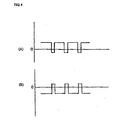
- Fig. 4 shows the waveforms of the pulse voltages generated on the coils L2 and L3 when a short circuit is caused on the secondary side of the transformer 25.
- an axis of abscissa indicates a time and an axis of ordinate indicates a voltage value.
- an electric potential is zero on the axis of abscissa, and the electric potential is positive on the upper side of the axis of abscissa and is negative on the lower side of the axis of abscissa.
- the waveform shown in Fig. 4A represents a change in the electric potential of the terminal 4 of the coil L2, which is a pulse voltage induced to the coil L2.
- the waveform shown in Fig. 4B represents a change in the electric potential of the terminal 6 of the coil L3, which is a pulse voltage induced to the coil L3.
- the pulse voltage induced to the coil L2 and the pulse voltage induced to the coil L3 make a phase difference of 180 degrees.
- the pulse width of the voltage induced to the coil L2 (the duty of the pulse voltage) is greater than the pulse width of the voltage induced to the coil L3 (the duty of the pulse voltage).
- the pulse voltage induced to the second coil L2 is integrated by the first integrating circuit 31. Moreover, the pulse voltage induced to the third coil L3 is integrated by the second integrating circuit 32.
- Fig. 5 shows voltages obtained by the integration of the first integrating circuit 31 and the second integrating circuit 32,
- an axis of abscissa indicates a time and an axis of ordinate indicates a voltage value.
- an electric potential is zero on the axis of abscissa, and the electric potential is positive on the upper side of the axis of abscissa.
- Fig. 5A shows the waveform of a voltage which is obtained after the integration of the first integrating circuit 31 and Fig. 5B shows the waveform of a voltage which is obtained after the integration of the second integrating circuit 32.
- the voltage obtained after the integration of the first integrating circuit 31 is changed into a smoothened voltage on a constant level having the voltage value V AB1 .
- the voltage obtained after the integration of the second integrating circuit 32 is changed into a smoothened voltage on a constant level having the voltage value V AB2.
- a voltage based on a difference between the Output V AB1 of the first integrating circuit 31 and the output V AB2 of the second integrating circuit 32 is applied in the opposite direction to the Zener diode 13, and is higher than the breakdown voltage Vtz in the opposite direction to the Zener diode 13. Consequently, the Zener diode 13 can be conducted in the opposite direction.
- the voltage V AB1 output from the first integrating circuit 31 and applied in the opposite direction to the Zener diode 13 is applied to the emitter terminal 14e of the transistor 14. Then, the transistor 14 is brought into the conduction state based on the difference between the voltages V AB1 and V AB2 .
- the voltage output from the collector terminal 14c of the transistor 14 is input to the base terminal 15b of the transistor 15 so that the transistor 15 is brought into the conduction state. Consequently, the collector terminal 15c and the emitter terminal 15e in the transistor 15 are brought into the conduction state and the collector terminal 15c is connected to the ground.
- the gate terminal 1g is grounded and a control voltage is not input so that the power FET 1 is brought into a non-conduction state. Therefore, a currant cannot be given to the coil L1 of the transformer 25 and the power FET 1 and a power cannot be supplied to the transformer 25. As a result, the operation of the power circuit 35 is stopped.
- the power circuit 35 does not need to comprise, on the secondary side, means for detecting that the abnormality is generated on the secondary side of the transformer 25. According to the power circuit 35, therefore, the size of the secondary side of the transformer 25 is decreased. Thus, it is possible to reduce a space for providing the power circuit 35.
- the size of the secondary side of the transformer 25 is decreased. Therefore, an electric apparatus can easily be connected to the secondary side of the transformer 25 and the power circuit 35 can readily be handled.
- the power FET is used as the power switching unit 1.
- the power switching unit 1 a unit other than the power FET.
- the power switching unit 1 is a switching unit which includes a control terminal, an input terminal and an output terminal, can input a current from the input terminal and can output the same current from the output terminal when a control voltage is input to the control terminal to bring a conduction state, and can input/output a large power.
- a power transistor as a power switching unit other than the power FET.
- NPN transistor is used as the first switching unit 15 in the above description, moreover, a PNP transistor can also be used as the first switching unit 15.
- the first switching unit 15 is a semiconductor switching unit other than a transistor. More specifically, it is sufficient that the first switching unit 15 is a switching unit which includes a terminal for inputting, as an operation signal, a voltage output from the second switching unit 14, a terminal to be connected to the output terminal of the power switching unit 1 and a terminal to be connected to the ground, and is brought into a conduction state by the input of the voltage from the second switching unit 14 and can thus conduct the output terminal of the power switching unit 1 to the ground.
- NFN transistor can also be used as the second switching unit 14.
- the second switching unit 14 is a semiconductor switching unit other than a transistor. More specifically, it is sufficient that the second switching unit 14 is a switching unit which includes a terminal for inputting a voltage output from the Zener diode 13, a terminal for inputting a voltage output from the second integrating circuit 32 and a terminal for outputting a voltage to the first switching unit 15, and is brought into a conduction state based on a difference between the voltage output from the abnormality detecting means 13 and the voltage output from the second integrating circuit 32, thereby controlling the first switching unit 15 to be brought into the conduction state.
- the abnormality detecting means 13 can detect the abnormality of the state of the voltage between the second coil L2 and the third coil L3 based on a predetermined set value in place of the Zener diode. It is sufficient that the second switching unit 14 can be brought into the conduction state and the first switching unit 15 can be thus brought into the conduction state when the abnormality of the voltage is detected by the abnormality detecting means 13.
- the second switching unit 14 is brought into the conduction state and the first switching unit 15 is thus brought into the conduction state when the abnormality detecting means 13 detects an abnormality.
- the means for detecting an abnormality generated on the secondary side of the transformer is provided on the primary side of the transformer and the size of the secondary side of the transformer is reduced. According to the power circuit of the present invention, consequently, it is possible to produce an advantage that a space for providing the power circuit can be reduced. Moreover, it is also possible to produce an advantage that an electric apparatus can easily be connected to the power circuit and the power circuit can readily be handled.
Landscapes
- Engineering & Computer Science (AREA)
- Power Engineering (AREA)
- Dc-Dc Converters (AREA)
- Emergency Protection Circuit Devices (AREA)
- Protection Of Static Devices (AREA)
Claims (6)
- Circuit de puissance comprenant un transformateur,- où une première bobine (L1), une seconde bobine (L2) et une troisième bobine (L3) sont pourvues sur un côté primaire du transformateur (25), une tension d'impulsions est appliquée à la première bobine (L1) d'une source d'énergie pour faire sortir une puissance basée sur la tension d'impulsions, chacune de la seconde (L2) et troisième bobine (L3) présente l'une des bornes liée à la masse en commun et les directions dans lesquelles les bobines vont être enroulées vers les autres bornes sont opposées l'une de l'autre et les nombres d'enroulements de la seconde et troisième bobine sont différents l'un de l'autre,- une pluralité de bobines correspondant à la première, la seconde et la troisième bobine sur le côté primaire sont pourvues sur un côté secondaire du transformateur (25),- le côté primaire du transformateur (25) est pourvu avec une unité de commutation de puissance (1) connectée en série à la première bobine (L1) et servant pour commander une entrée d'une puissance au transformateur (25), un premier circuit intégré (31) pour intégrer une sortie de tension par une diode connectée à l'autre borne de la seconde bobine (L2) dans une direction de passage, un second circuit intégré (32) pour intégrer une sortie de tension par une diode connectée à l'autre borne de la troisième bobine (L3) dans une direction de passage, et des moyens de détection d'anomalies (13) pour détecter une anomalie d'un état d'une tension entre la seconde bobine (L2) et la troisième bobine (L3) basée sur une sortie du premier circuit intégré (31), une sortie du second circuit intégré (32) et une valeur prédéterminée établie,- une tension d'impulsions est appliquée à la première bobine (L1) de sorte qu'une puissance soit introduite au transformateur (25) quand l'unité de commutation de puissance est amenée dans un état de conduction, et- l'unité de commutation de puissance (1) est amenée dans un état de non-conduction de sorte que l'entrée de la puissance au transformateur (25) est stoppée quand le moyen de détection d'anomalies (13) détecte l'anomalie de l'état de la tension entre la seconde bobine (L2) et la troisième bobine (L3).
- Circuit de puissance selon la revendication 1, où une première unité de commutation pour commander un actionnement de l'unité de commutation de puissance (1) est pourvue sur le côté primaire du transformateur (25),- l'unité de commutation de puissance (1) présente une borne d'entrée pour introduire un courant et une borne de sortie pour faire sortir le courant qui sont connectées en série à la première bobine (L1), et une borne de commande pour commander un état de conduction et un état de non-conduction qui est connectée pour introduire une tension de commande à partir de l'autre borne de la seconde bobine (L2) et est connectée à la masse par la première unité de commutation, et- la première unité de commutation est amenée dans l'état de conduction quand le moyen de détection d'anomalies (13) détecte l'anomalie, la borne de commande de l'unité de commutation de puissance (1) est liée à la masse par la première unité de commutation configurée dans l'état de conduction, et l'unité de commutation de puissance (1) est ainsi amenée dans l'état de non-conduction.
- Circuit de puissance selon la revendication 2, où une diode Zener est pourvue comme le moyen de détection d'anomalies (13), la diode Zener est conduite dans une direction opposée quand une anomalie est générée sur l'état de la tension entre la seconde bobine (L2) et la troisième bobine (L3), et la diode Zener conduite dans la direction opposée fait sortir une tension, de cette manière amenant la première unité de commutation (1) dans l'état de conduction.
- Circuit de puissance selon la revendication 3, où le côté primaire du transformateur (25) est pourvu avec une seconde unité de commutation pour commander l'état de conduction de la première unité de commutation,- la seconde unité de commutation est connectée pour être amenée dans l'état de conduction quand la diode Zener détecte l'anomalie de l'état de la tension entre la seconde bobine (L2) et la troisième bobine (L3), de cette manière faisant sortir une tension, et- la première unité de commutation est amenée dans l'état de conduction par la seconde unité de commutation configurée dans l'état de conduction.
- Circuit de puissance selon l'une quelconque des revendications 1 à 4, où la première unité de commutation est un transistor.
- Circuit de puissance selon la revendication 4 ou 5, où la seconde unité de commutation est un transistor.
Applications Claiming Priority (2)
| Application Number | Priority Date | Filing Date | Title |
|---|---|---|---|
| JP2002282662 | 2002-09-27 | ||
| JP2002282662A JP3656911B2 (ja) | 2002-09-27 | 2002-09-27 | 電源回路 |
Publications (3)
| Publication Number | Publication Date |
|---|---|
| EP1404014A2 EP1404014A2 (fr) | 2004-03-31 |
| EP1404014A3 EP1404014A3 (fr) | 2004-12-22 |
| EP1404014B1 true EP1404014B1 (fr) | 2007-03-07 |
Family
ID=31973334
Family Applications (1)
| Application Number | Title | Priority Date | Filing Date |
|---|---|---|---|
| EP03022105A Expired - Lifetime EP1404014B1 (fr) | 2002-09-27 | 2003-09-29 | Circuit de puissance |
Country Status (4)
| Country | Link |
|---|---|
| US (1) | US6865095B2 (fr) |
| EP (1) | EP1404014B1 (fr) |
| JP (1) | JP3656911B2 (fr) |
| DE (1) | DE60312275T2 (fr) |
Families Citing this family (4)
| Publication number | Priority date | Publication date | Assignee | Title |
|---|---|---|---|---|
| JP2012239277A (ja) | 2011-05-11 | 2012-12-06 | Funai Electric Co Ltd | 電子機器 |
| DE102012111061A1 (de) * | 2012-11-16 | 2014-05-22 | Phoenix Contact Gmbh & Co. Kg | Schutzschaltung für einen Stromwandler und Stromwandler mit einer Schutzschaltung |
| US9430012B2 (en) * | 2012-12-11 | 2016-08-30 | General Electric Company | Systems and methods of transformer failure detection and control |
| JP6177422B2 (ja) * | 2014-02-26 | 2017-08-09 | 三菱電機株式会社 | アクティブバラン回路及びトランス |
Family Cites Families (13)
| Publication number | Priority date | Publication date | Assignee | Title |
|---|---|---|---|---|
| JPS60187260A (ja) * | 1984-03-02 | 1985-09-24 | Matsushita Electric Ind Co Ltd | 自励発振式スイツチング電源装置 |
| IT1188718B (it) * | 1986-05-22 | 1988-01-28 | Neywell Information Systems It | Alimentatore a commutazione |
| JPH0442774A (ja) * | 1990-06-05 | 1992-02-13 | Murata Mfg Co Ltd | スイッチング電源装置 |
| JPH0518291A (ja) | 1991-07-09 | 1993-01-26 | Nippondenso Co Ltd | 燃料噴射装置 |
| JPH0622537A (ja) | 1992-07-06 | 1994-01-28 | Matsushita Electric Ind Co Ltd | 高圧電源保護装置 |
| JP3433429B2 (ja) | 1992-07-24 | 2003-08-04 | 株式会社村田製作所 | スイッチングレギュレータ |
| JPH0690559A (ja) | 1992-09-07 | 1994-03-29 | Murata Mfg Co Ltd | 電源回路 |
| JPH07227083A (ja) * | 1994-02-08 | 1995-08-22 | Hitachi Ltd | 短絡保護回路 |
| JP2806283B2 (ja) | 1994-12-12 | 1998-09-30 | ヤマハ株式会社 | スイッチング電源回路 |
| JP3261646B2 (ja) | 1995-04-13 | 2002-03-04 | 大平電子株式会社 | 自励式スイッチング電源装置 |
| US5796596A (en) * | 1996-11-15 | 1998-08-18 | Thomson Consumer Electronics, Inc. | Fault control circuit for switched power supply |
| JPH1198838A (ja) | 1997-09-19 | 1999-04-09 | Matsushita Electric Ind Co Ltd | 電流制御型スイッチング電源 |
| JPH11164551A (ja) | 1997-11-28 | 1999-06-18 | Sony Corp | スイッチング電源装置 |
-
2002
- 2002-09-27 JP JP2002282662A patent/JP3656911B2/ja not_active Expired - Fee Related
-
2003
- 2003-09-29 DE DE60312275T patent/DE60312275T2/de not_active Expired - Fee Related
- 2003-09-29 US US10/671,476 patent/US6865095B2/en not_active Expired - Fee Related
- 2003-09-29 EP EP03022105A patent/EP1404014B1/fr not_active Expired - Lifetime
Also Published As
| Publication number | Publication date |
|---|---|
| DE60312275D1 (de) | 2007-04-19 |
| EP1404014A2 (fr) | 2004-03-31 |
| US6865095B2 (en) | 2005-03-08 |
| EP1404014A3 (fr) | 2004-12-22 |
| US20040095783A1 (en) | 2004-05-20 |
| JP2004120926A (ja) | 2004-04-15 |
| JP3656911B2 (ja) | 2005-06-08 |
| DE60312275T2 (de) | 2007-11-08 |
Similar Documents
| Publication | Publication Date | Title |
|---|---|---|
| US6975523B2 (en) | Power supply capable of protecting electric device circuit | |
| US7964988B2 (en) | Lighting controller of lighting device for vehicle | |
| KR101026441B1 (ko) | 차량용 등기구의 점등 제어 장치 | |
| US6496395B2 (en) | Direct-current power-supply apparatus, control circuit thereof and semiconductor integrated circuit device for power supply | |
| US6137696A (en) | Switching regulator for power converter with dual mode feedback input and method thereof | |
| TWI414142B (zh) | 電源供應控制方法及其系統 | |
| US11563371B2 (en) | Switching control circuit and power supply circuit | |
| EP1058176B1 (fr) | Unité d'alimentation et système d'alimentation | |
| US9603227B2 (en) | Semiconductor light source driving apparatus | |
| US7375990B2 (en) | Switching power device | |
| EP1404014B1 (fr) | Circuit de puissance | |
| US5369307A (en) | Switching power source | |
| US6611436B2 (en) | Switching power supply unit having a regulator circuit and electronic apparatus using the same | |
| US20060023477A1 (en) | Electronic apparatus | |
| US20040174721A1 (en) | Switching power supply unit | |
| US7542309B2 (en) | Voltage stabilizer circuit of forward converter | |
| KR101284827B1 (ko) | 스위치 제어 장치, 스위치 제어 방법 및 이를 이용하는컨버터 | |
| JP4356396B2 (ja) | 電圧生成回路およびこれを備えたスイッチング電源 | |
| US7960952B2 (en) | Switching mode power supply and switch thereof | |
| JPH09215331A (ja) | スイッチング電源装置 | |
| US20070114980A1 (en) | Autonomous switching transformer | |
| US20220360208A1 (en) | Motor unit | |
| KR100236645B1 (ko) | 마이콤을 이용한 정전압 회로 | |
| KR19990066316A (ko) | 과전압 보호회로를 갖는 스위칭모드 전원공급장치 | |
| KR0111805Y1 (ko) | 입력 페일신호 출력회로 |
Legal Events
| Date | Code | Title | Description |
|---|---|---|---|
| PUAI | Public reference made under article 153(3) epc to a published international application that has entered the european phase |
Free format text: ORIGINAL CODE: 0009012 |
|
| AK | Designated contracting states |
Kind code of ref document: A2 Designated state(s): AT BE BG CH CY CZ DE DK EE ES FI FR GB GR HU IE IT LI LU MC NL PT RO SE SI SK TR |
|
| AX | Request for extension of the european patent |
Extension state: AL LT LV MK |
|
| RIN1 | Information on inventor provided before grant (corrected) |
Inventor name: TANI, KATSUHIKO |
|
| PUAL | Search report despatched |
Free format text: ORIGINAL CODE: 0009013 |
|
| AK | Designated contracting states |
Kind code of ref document: A3 Designated state(s): AT BE BG CH CY CZ DE DK EE ES FI FR GB GR HU IE IT LI LU MC NL PT RO SE SI SK TR |
|
| AX | Request for extension of the european patent |
Extension state: AL LT LV MK |
|
| 17P | Request for examination filed |
Effective date: 20050613 |
|
| AKX | Designation fees paid |
Designated state(s): DE FR GB IT |
|
| GRAP | Despatch of communication of intention to grant a patent |
Free format text: ORIGINAL CODE: EPIDOSNIGR1 |
|
| GRAS | Grant fee paid |
Free format text: ORIGINAL CODE: EPIDOSNIGR3 |
|
| GRAA | (expected) grant |
Free format text: ORIGINAL CODE: 0009210 |
|
| AK | Designated contracting states |
Kind code of ref document: B1 Designated state(s): DE FR GB IT |
|
| REG | Reference to a national code |
Ref country code: GB Ref legal event code: FG4D |
|
| REF | Corresponds to: |
Ref document number: 60312275 Country of ref document: DE Date of ref document: 20070419 Kind code of ref document: P |
|
| ET | Fr: translation filed | ||
| PLBE | No opposition filed within time limit |
Free format text: ORIGINAL CODE: 0009261 |
|
| STAA | Information on the status of an ep patent application or granted ep patent |
Free format text: STATUS: NO OPPOSITION FILED WITHIN TIME LIMIT |
|
| 26N | No opposition filed |
Effective date: 20071210 |
|
| PG25 | Lapsed in a contracting state [announced via postgrant information from national office to epo] |
Ref country code: IT Free format text: LAPSE BECAUSE OF FAILURE TO SUBMIT A TRANSLATION OF THE DESCRIPTION OR TO PAY THE FEE WITHIN THE PRESCRIBED TIME-LIMIT Effective date: 20070307 |
|
| GBPC | Gb: european patent ceased through non-payment of renewal fee |
Effective date: 20070929 |
|
| PG25 | Lapsed in a contracting state [announced via postgrant information from national office to epo] |
Ref country code: DE Free format text: LAPSE BECAUSE OF NON-PAYMENT OF DUE FEES Effective date: 20080401 |
|
| REG | Reference to a national code |
Ref country code: FR Ref legal event code: ST Effective date: 20080531 |
|
| PG25 | Lapsed in a contracting state [announced via postgrant information from national office to epo] |
Ref country code: FR Free format text: LAPSE BECAUSE OF NON-PAYMENT OF DUE FEES Effective date: 20071001 |
|
| PG25 | Lapsed in a contracting state [announced via postgrant information from national office to epo] |
Ref country code: GB Free format text: LAPSE BECAUSE OF NON-PAYMENT OF DUE FEES Effective date: 20070929 |