EP1394860B1 - Leistungsanordnungen mit verbesserten Durchbruchsspannungen - Google Patents
Leistungsanordnungen mit verbesserten Durchbruchsspannungen Download PDFInfo
- Publication number
- EP1394860B1 EP1394860B1 EP03018788.4A EP03018788A EP1394860B1 EP 1394860 B1 EP1394860 B1 EP 1394860B1 EP 03018788 A EP03018788 A EP 03018788A EP 1394860 B1 EP1394860 B1 EP 1394860B1
- Authority
- EP
- European Patent Office
- Prior art keywords
- region
- substrate
- doped
- isolation diffusion
- junction
- Prior art date
- Legal status (The legal status is an assumption and is not a legal conclusion. Google has not performed a legal analysis and makes no representation as to the accuracy of the status listed.)
- Expired - Lifetime
Links
- 230000015556 catabolic process Effects 0.000 title description 25
- 239000000758 substrate Substances 0.000 claims description 65
- 238000002955 isolation Methods 0.000 claims description 61
- 238000009792 diffusion process Methods 0.000 claims description 58
- ZOXJGFHDIHLPTG-UHFFFAOYSA-N Boron Chemical compound [B] ZOXJGFHDIHLPTG-UHFFFAOYSA-N 0.000 claims description 26
- 229910052796 boron Inorganic materials 0.000 claims description 26
- 230000002093 peripheral effect Effects 0.000 claims description 24
- XAGFODPZIPBFFR-UHFFFAOYSA-N aluminium Chemical compound [Al] XAGFODPZIPBFFR-UHFFFAOYSA-N 0.000 claims description 22
- 229910052782 aluminium Inorganic materials 0.000 claims description 22
- 238000002161 passivation Methods 0.000 claims description 20
- 239000004065 semiconductor Substances 0.000 claims description 10
- 229920001721 polyimide Polymers 0.000 claims description 3
- 239000004642 Polyimide Substances 0.000 claims 2
- 239000004411 aluminium Substances 0.000 claims 2
- 230000000903 blocking effect Effects 0.000 description 38
- 239000011521 glass Substances 0.000 description 15
- 239000002019 doping agent Substances 0.000 description 13
- 230000005684 electric field Effects 0.000 description 11
- 235000012431 wafers Nutrition 0.000 description 9
- 238000000034 method Methods 0.000 description 8
- 230000000694 effects Effects 0.000 description 4
- 238000011109 contamination Methods 0.000 description 3
- 230000007423 decrease Effects 0.000 description 3
- 239000003989 dielectric material Substances 0.000 description 3
- 238000005516 engineering process Methods 0.000 description 3
- 238000001465 metallisation Methods 0.000 description 3
- 229910052581 Si3N4 Inorganic materials 0.000 description 2
- XUIMIQQOPSSXEZ-UHFFFAOYSA-N Silicon Chemical compound [Si] XUIMIQQOPSSXEZ-UHFFFAOYSA-N 0.000 description 2
- 238000005452 bending Methods 0.000 description 2
- 230000015572 biosynthetic process Effects 0.000 description 2
- 229910052799 carbon Inorganic materials 0.000 description 2
- 238000006731 degradation reaction Methods 0.000 description 2
- 230000009977 dual effect Effects 0.000 description 2
- 230000005611 electricity Effects 0.000 description 2
- 238000002347 injection Methods 0.000 description 2
- 239000007924 injection Substances 0.000 description 2
- 238000004519 manufacturing process Methods 0.000 description 2
- 229910021420 polycrystalline silicon Inorganic materials 0.000 description 2
- 229920005591 polysilicon Polymers 0.000 description 2
- 230000002028 premature Effects 0.000 description 2
- 229910052710 silicon Inorganic materials 0.000 description 2
- 239000010703 silicon Substances 0.000 description 2
- HQVNEWCFYHHQES-UHFFFAOYSA-N silicon nitride Chemical compound N12[Si]34N5[Si]62N3[Si]51N64 HQVNEWCFYHHQES-UHFFFAOYSA-N 0.000 description 2
- 238000004088 simulation Methods 0.000 description 2
- 230000001419 dependent effect Effects 0.000 description 1
- 230000005669 field effect Effects 0.000 description 1
- 238000002513 implantation Methods 0.000 description 1
- 230000035945 sensitivity Effects 0.000 description 1
- 239000007921 spray Substances 0.000 description 1
Images


Classifications
-
- H—ELECTRICITY
- H01—ELECTRIC ELEMENTS
- H01L—SEMICONDUCTOR DEVICES NOT COVERED BY CLASS H10
- H01L29/00—Semiconductor devices specially adapted for rectifying, amplifying, oscillating or switching and having potential barriers; Capacitors or resistors having potential barriers, e.g. a PN-junction depletion layer or carrier concentration layer; Details of semiconductor bodies or of electrodes thereof ; Multistep manufacturing processes therefor
- H01L29/02—Semiconductor bodies ; Multistep manufacturing processes therefor
- H01L29/06—Semiconductor bodies ; Multistep manufacturing processes therefor characterised by their shape; characterised by the shapes, relative sizes, or dispositions of the semiconductor regions ; characterised by the concentration or distribution of impurities within semiconductor regions
- H01L29/08—Semiconductor bodies ; Multistep manufacturing processes therefor characterised by their shape; characterised by the shapes, relative sizes, or dispositions of the semiconductor regions ; characterised by the concentration or distribution of impurities within semiconductor regions with semiconductor regions connected to an electrode carrying current to be rectified, amplified or switched and such electrode being part of a semiconductor device which comprises three or more electrodes
- H01L29/083—Anode or cathode regions of thyristors or gated bipolar-mode devices
- H01L29/0834—Anode regions of thyristors or gated bipolar-mode devices, e.g. supplementary regions surrounding anode regions
-
- H—ELECTRICITY
- H01—ELECTRIC ELEMENTS
- H01L—SEMICONDUCTOR DEVICES NOT COVERED BY CLASS H10
- H01L29/00—Semiconductor devices specially adapted for rectifying, amplifying, oscillating or switching and having potential barriers; Capacitors or resistors having potential barriers, e.g. a PN-junction depletion layer or carrier concentration layer; Details of semiconductor bodies or of electrodes thereof ; Multistep manufacturing processes therefor
- H01L29/02—Semiconductor bodies ; Multistep manufacturing processes therefor
- H01L29/06—Semiconductor bodies ; Multistep manufacturing processes therefor characterised by their shape; characterised by the shapes, relative sizes, or dispositions of the semiconductor regions ; characterised by the concentration or distribution of impurities within semiconductor regions
- H01L29/0603—Semiconductor bodies ; Multistep manufacturing processes therefor characterised by their shape; characterised by the shapes, relative sizes, or dispositions of the semiconductor regions ; characterised by the concentration or distribution of impurities within semiconductor regions characterised by particular constructional design considerations, e.g. for preventing surface leakage, for controlling electric field concentration or for internal isolations regions
- H01L29/0607—Semiconductor bodies ; Multistep manufacturing processes therefor characterised by their shape; characterised by the shapes, relative sizes, or dispositions of the semiconductor regions ; characterised by the concentration or distribution of impurities within semiconductor regions characterised by particular constructional design considerations, e.g. for preventing surface leakage, for controlling electric field concentration or for internal isolations regions for preventing surface leakage or controlling electric field concentration
- H01L29/0611—Semiconductor bodies ; Multistep manufacturing processes therefor characterised by their shape; characterised by the shapes, relative sizes, or dispositions of the semiconductor regions ; characterised by the concentration or distribution of impurities within semiconductor regions characterised by particular constructional design considerations, e.g. for preventing surface leakage, for controlling electric field concentration or for internal isolations regions for preventing surface leakage or controlling electric field concentration for increasing or controlling the breakdown voltage of reverse biased devices
- H01L29/0615—Semiconductor bodies ; Multistep manufacturing processes therefor characterised by their shape; characterised by the shapes, relative sizes, or dispositions of the semiconductor regions ; characterised by the concentration or distribution of impurities within semiconductor regions characterised by particular constructional design considerations, e.g. for preventing surface leakage, for controlling electric field concentration or for internal isolations regions for preventing surface leakage or controlling electric field concentration for increasing or controlling the breakdown voltage of reverse biased devices by the doping profile or the shape or the arrangement of the PN junction, or with supplementary regions, e.g. junction termination extension [JTE]
- H01L29/0619—Semiconductor bodies ; Multistep manufacturing processes therefor characterised by their shape; characterised by the shapes, relative sizes, or dispositions of the semiconductor regions ; characterised by the concentration or distribution of impurities within semiconductor regions characterised by particular constructional design considerations, e.g. for preventing surface leakage, for controlling electric field concentration or for internal isolations regions for preventing surface leakage or controlling electric field concentration for increasing or controlling the breakdown voltage of reverse biased devices by the doping profile or the shape or the arrangement of the PN junction, or with supplementary regions, e.g. junction termination extension [JTE] with a supplementary region doped oppositely to or in rectifying contact with the semiconductor containing or contacting region, e.g. guard rings with PN or Schottky junction
-
- H—ELECTRICITY
- H01—ELECTRIC ELEMENTS
- H01L—SEMICONDUCTOR DEVICES NOT COVERED BY CLASS H10
- H01L29/00—Semiconductor devices specially adapted for rectifying, amplifying, oscillating or switching and having potential barriers; Capacitors or resistors having potential barriers, e.g. a PN-junction depletion layer or carrier concentration layer; Details of semiconductor bodies or of electrodes thereof ; Multistep manufacturing processes therefor
- H01L29/66—Types of semiconductor device ; Multistep manufacturing processes therefor
- H01L29/68—Types of semiconductor device ; Multistep manufacturing processes therefor controllable by only the electric current supplied, or only the electric potential applied, to an electrode which does not carry the current to be rectified, amplified or switched
- H01L29/70—Bipolar devices
- H01L29/72—Transistor-type devices, i.e. able to continuously respond to applied control signals
- H01L29/739—Transistor-type devices, i.e. able to continuously respond to applied control signals controlled by field-effect, e.g. bipolar static induction transistors [BSIT]
- H01L29/7393—Insulated gate bipolar mode transistors, i.e. IGBT; IGT; COMFET
- H01L29/7395—Vertical transistors, e.g. vertical IGBT
-
- H—ELECTRICITY
- H01—ELECTRIC ELEMENTS
- H01L—SEMICONDUCTOR DEVICES NOT COVERED BY CLASS H10
- H01L29/00—Semiconductor devices specially adapted for rectifying, amplifying, oscillating or switching and having potential barriers; Capacitors or resistors having potential barriers, e.g. a PN-junction depletion layer or carrier concentration layer; Details of semiconductor bodies or of electrodes thereof ; Multistep manufacturing processes therefor
- H01L29/66—Types of semiconductor device ; Multistep manufacturing processes therefor
- H01L29/68—Types of semiconductor device ; Multistep manufacturing processes therefor controllable by only the electric current supplied, or only the electric potential applied, to an electrode which does not carry the current to be rectified, amplified or switched
- H01L29/70—Bipolar devices
- H01L29/74—Thyristor-type devices, e.g. having four-zone regenerative action
-
- H—ELECTRICITY
- H01—ELECTRIC ELEMENTS
- H01L—SEMICONDUCTOR DEVICES NOT COVERED BY CLASS H10
- H01L29/00—Semiconductor devices specially adapted for rectifying, amplifying, oscillating or switching and having potential barriers; Capacitors or resistors having potential barriers, e.g. a PN-junction depletion layer or carrier concentration layer; Details of semiconductor bodies or of electrodes thereof ; Multistep manufacturing processes therefor
- H01L29/66—Types of semiconductor device ; Multistep manufacturing processes therefor
- H01L29/86—Types of semiconductor device ; Multistep manufacturing processes therefor controllable only by variation of the electric current supplied, or only the electric potential applied, to one or more of the electrodes carrying the current to be rectified, amplified, oscillated or switched
- H01L29/861—Diodes
-
- H—ELECTRICITY
- H01—ELECTRIC ELEMENTS
- H01L—SEMICONDUCTOR DEVICES NOT COVERED BY CLASS H10
- H01L29/00—Semiconductor devices specially adapted for rectifying, amplifying, oscillating or switching and having potential barriers; Capacitors or resistors having potential barriers, e.g. a PN-junction depletion layer or carrier concentration layer; Details of semiconductor bodies or of electrodes thereof ; Multistep manufacturing processes therefor
- H01L29/02—Semiconductor bodies ; Multistep manufacturing processes therefor
- H01L29/06—Semiconductor bodies ; Multistep manufacturing processes therefor characterised by their shape; characterised by the shapes, relative sizes, or dispositions of the semiconductor regions ; characterised by the concentration or distribution of impurities within semiconductor regions
- H01L29/0603—Semiconductor bodies ; Multistep manufacturing processes therefor characterised by their shape; characterised by the shapes, relative sizes, or dispositions of the semiconductor regions ; characterised by the concentration or distribution of impurities within semiconductor regions characterised by particular constructional design considerations, e.g. for preventing surface leakage, for controlling electric field concentration or for internal isolations regions
- H01L29/0607—Semiconductor bodies ; Multistep manufacturing processes therefor characterised by their shape; characterised by the shapes, relative sizes, or dispositions of the semiconductor regions ; characterised by the concentration or distribution of impurities within semiconductor regions characterised by particular constructional design considerations, e.g. for preventing surface leakage, for controlling electric field concentration or for internal isolations regions for preventing surface leakage or controlling electric field concentration
- H01L29/0638—Semiconductor bodies ; Multistep manufacturing processes therefor characterised by their shape; characterised by the shapes, relative sizes, or dispositions of the semiconductor regions ; characterised by the concentration or distribution of impurities within semiconductor regions characterised by particular constructional design considerations, e.g. for preventing surface leakage, for controlling electric field concentration or for internal isolations regions for preventing surface leakage or controlling electric field concentration for preventing surface leakage due to surface inversion layer, e.g. with channel stopper
Definitions
- the present invention relates to integrated circuit devices, and in particular high voltage thyristors, and diodes ("power devices").
- a power device is a device that is capable of handling currents in excess of 1 A and/or handles 50 volts or more. Some power devices are configured to handle 10 kA or more and/or 4 kV. Generally, power devices handle few hundred volts or more.
- the power device may be two terminal devices, e.g., diodes, or three terminal devices, e.g., transistors. In the three terminal devices, the control terminals (e.g., base or gate) determines the characteristics of the conduction path between the two other terminals or conduction terminals. These terminals are the emitter and collector in the bipolar transistor, and the source and drain in the field-effect transistor, and the anode and cathode in the thryristors.
- the control function can be exercised either by the injection of current or through the voltage of the control electrode. If the injection of current is used the control electrode makes a direct contact with the semiconductor substrate. If the voltages of the control electrode is used, the control electrode is separated from the substrate by a dielectric layer to prevent current flow between the control electrode and the substrate.
- EP 1 098 355 A1 describes a power component formed in a substrate of first conductivity type, which is delimited by an isolation wall of second conductivity type.
- the isolation wall extends from the upper to the lower surface of the substrate.
- First and second thyristors are arranged between an upper surface side metallization and a lower surface side metallization.
- Channel stop regions are arranged on the upper surface side.
- EP 0 521 558 A2 discloses a semiconductor device comprising a substrate with an island-shaped region adjoining the surface of the substrate and forming a pn-junction with an adjoining insulating region extending from the upper to the lower surface of the substrate.
- the insulating region comprises a lateral extension and guard rings are provided for increasing the breakdown voltage of the pn-junction.
- the power devices are rated according to their blocking voltage capability. Generally, there are two types of blocking voltages: forward blocking voltage and reverse blocking voltage. Regardless of the types of the power devices, there is a great interest in providing a power device that has an improved forward blocking voltage or reverse blocking voltage, or both since such a device would tend to be more robust and could be used in wider applications.
- Fig. 1 shows a conventional power device which is not part of the invention.
- Fig. 2 shows a cross-sectional view of an IGBT device which is not part of the invention.
- Fig. 3 shows a power device configured to handle relatively high forward and reverse blocking voltages which is not part of the invention.
- Fig. 4 illustrates a diode which is not part of the invention.
- Fig. 5 illustrates a thrysistor which is not part of the invention.
- Fig. 6 illustrates a power device which is not part of the invention.
- Fig. 7 illustrates a power device configured to handle high forward and reverse blocking voltages according to one embodiment of the present invention.
- Fig. 8 illustrates a power device that has a plurality of shallow junction guard rings according to the invention.
- Fig. 9A shows potential contours for a power with the shallow junction extension (JE) region and fixed oxide charge of 1E11 cm -2 .
- Fig. 9B shows a power device without the shallow junction extension (JE) region.
- Fig. 10 illustrates forward breakdown voltage graphs associated with a device having the first shallow junction region and shallow junction guard rings.
- Figs. 11A-11C illustrate a simulation performed with respect to the forward blocking voltage on a power device.
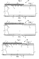
- Fig. 1 shows a conventional power device 50, also referred to as a silicon controlled rectifier (SCR) or thyristor.
- the device 50 includes an isolation diffusion region 2 that extends from an upper surface 3 and a lower surface 4 of a semiconductor substrate 1.
- a glass passivation layer 17 is provided on the upper surface of the substrate to prevent contamination or damage to the device. Other dielectric materials may be used.
- a channel stopper 14 and a plurality of guard rings 8 are provided on the upper surface.
- the channel stopper is an N+ type region.
- the guard rings are P+ regions.
- a conductive regions 5 and 15 are provided on the upper surface and the lower surface, respectively, of the substrate.
- the conductive regions 5 and 15 are P+ regions.
- a cathode 7 is formed on the upper surface.
- An anode 16 is formed on the lower surface.
- the anode and cathode are formed from aluminum.
- N- type region As used herein, the terms "N- type region,” “N type region,” and “N+ type region” are terms used to described the relative dopant concentration levels of the conductive regions in a given power device. That is, the term “N+ type region” indicates that that regions has a higher dopant concentration level than the "N type region.” Accordingly, no maximum or minimum concentration levels should be read into the use of these terms. Similarly, no maximum or minimum concentration levels should be read into the use of terms "P type region” and "P+ type region.”
- the device provides a forward blocking voltage that is about 85% of the bulk breakdown voltage and a reverse blocking voltage that is about 95% of the bulk breakdown voltage with less leakage current.
- the reverse blocking voltage reduces to 60% of the bulk breakdown voltage with an increased leakage current if oxide and polyimid layers are used as a passivation layer.
- Fig. 2 shows a cross-sectional view of an IGBT device 52 which is not part of the invention.
- the IGBT device may be formed by a double diffused MOS process (DMOS) and the like.
- the device 52 includes an N+ type semiconductor substrate 101.
- An N- type layer 103 is formed overlying the N+ type semiconductor substrate 101.
- the N- type layer 103 is often an epitaxial layer or the like.
- P/P+ type well regions 105 are defined on the N- type layer 103.
- the device also includes a plurality of N type source regions 107 defined into a perimeter of each P/P+ type well region 105.
- a gate polysilicon layer (G) 109 is defined overlying a thin layer of gate oxide 111 and the like.
- Source metallization 113 is defined overlying the N type source regions 107, and connects 108 each source region together.
- a P type diffusion region 116 is defined overlying the backside of the N+ type substrate. The P type diffusion region is a P+ type drain region.
- a channel region 118 is defined in a portion of the P/P+ type well region between the source region 107 and a portion of the N- type layer 103.
- the device includes a plurality of guard ring structures 115.
- the guard ring structures are P type regions, typically surrounding the periphery of the integrated circuit chip active cell region to increase the forward blocking voltage of the device.
- a field plate (not shown) made of polysilicon is often defined overlying the guard ring structures.
- the guard ring structure tends to keep the main conduction region toward the active cell region of the integrated circuit chip, thereby preserving the voltage rating of the device.
- boron is used as the dopant for the guard ring.
- An isolation diffusion region or P type region 117 defines the scribe line of the device.
- Aluminum is used to form the isolation region due to its high mobility rate.
- boron may be used for formation of the upper portion of the isolation region, and aluminum is used for formation of the lower portion of the isolation region.
- the isolation region 117 creates a "wrap around" P type envelope covering sides of the die including the bottom P+ type drain region.
- the region 117 is provided to eliminates the exposed P+/N+junction and increase the reverse blocking voltage of the device. This device generally does not provide a high blocking voltage due to the presence of N+ buffer layer 101.
- the inventor also noted that the use of the oxide and polymid rather than glass as the passivation layer on the device 52 resulted in reduced reverse blocking voltages and increased leakage currents.
- the power devices configured to handle high forward and reverse blocking voltages use glass as the passivation layer.
- the power devices With the glass passivation, the power devices are provided with high forward and reverse blocking voltages and low leakage current (e.g., less than 500 micro amps at room temperature). Glass has low fixed charges so it does not influence the low surface concentration of isolation diffusion that results in low leakage current at breakdown.
- the glass passivation may not be used for wafer size greater than 5 inch, e.g., 6 inch or greater.
- the present inventors noted that wafers processed with glass passivation showed tendency to bend id 6 inch wafer were used. This bending problem results from the differences between the thermal expansion coefficients of the glass and silicon wafer. The bending is not a significant issue under the current state of art, which uses 5 inch wafer, for fabricating power devices. An appropriate substitute for glass would be needed in order to migrate to 6 inch or 8 inch wafers.
- the glass passivation is sensitive to the humidity and requires higher manufacturing costs since separate equipment is need to spray on the glass to the wafer.
- oxide and polymid One possible substitute is the oxide and polymid.
- an oxide layer is formed on the substrate and then a polymid layer is deposited on the oxide layer to form a two-layer passivation.
- the forward blocking voltage is not effected, the use of the oxide and polymid as the passivation layer causes the reverse blocking voltage to be lowered due to relatively high fixed charges associated with the oxide layer. That is, the reverse blocking voltage decreases with the increase in oxide charge since the impact ionization rate increases at the PN junction defined at the upper portion of the isolation diffusion region with the increase in oxide charge.
- Table A shows the influence of oxide charge on the reverse blocking voltages for an exemplary thyristor, such as that illustrated in Fig. 1 and fabricated with the parameters provided in Table B.
- an increased leakage current was detected, e.g., more than 5 mA at room temperature.
- the present inventor believes that the increase in leakage current is due to surface depletion of aluminum isolation region (diffusion zone) and relatively high fixed charge of the oxide. The surface depletion results from the long diffusion step used to diffuse aluminum into the substrate, so that relatively low concentration of aluminum exists on the surface.
- high concentration of boron is introduced into the isolation region in order to reduce the leakage current and increase the reverse blocking voltage.
- concentration of the boron may be varied according to the application.
- a single guard ring provided between the isolation diffusion region and channel stopper to reduce the electric field at the PN junction of isolation diffusion and increase the breakdown voltage.
- a plurality of guard rings are provided between the channel stopper and isolation diffusion regions. The plurality of guard rings may be shallow guard rings that are formed using a separate implantation/diffusion step from that used to form the conventional guard rings 8.
- the features of the present embodiments described herein relates to fabrication of power devices using 6 inch wafer or greater using a passivation layer that is not made of glass.
- a passivation layer that is not made of glass.
- the glass passivation are the oxide/polymid passivation, the oxide/silicon nitride/polymid passivation, and the diamond-like-carbon/polymid passivation.
- the present embodiments may also be implemented using glass passivation technology or glass/polymid technology, or 5 inch wafer technology, or the like.
- Fig. 3 shows a power device 54 which is not part of the invention configured to handle relatively high forward and reverse blocking voltages.
- the device 54 is a thyristor like the device 50 and has similar structures. Accordingly, the same numerals are used to denote the corresponding structures in the two devices.
- an n+ region 7(b) is defined inside the layer 5 for a thyristor.
- the device 54 includes an isolation diffusion region 2 that extends from an upper surface 3 to a lower surface 4 of a semiconductor substrate 1.
- the substrate has resistivity of about 77 Ohm-cm (5.57 X 10 13 cm 3 ) and has thickness of about 380 ⁇ m.
- the surface concentration of the isolation diffusion region is formed by diffusing aluminum vertically into the substrate from the upper and lower surfaces of the substrate. Surface concentration of the isolation diffusion region is provided to be about 1 X 10 17 cm -3 .
- the lateral aluminum diffusion is about 0.7 times the aluminum junction depth. In one embodiment, two more dopants may be used to form the isolation diffusion region, e.g., use boron to form an upper portion of the isolation region and aluminum to form a lower portion of the isolation region.
- An oxide layer 11 and a polymid layer 12 are provided on the upper surface of the substrate as dual passivation layers to prevent contamination or damage to the device.
- Other dielectric materials may be used.
- a plurality of guard rings 8 are provided on the upper surface of the substrate.
- the guard rings are P+ regions and are provided to increase the forward blocking voltage of the device.
- the guard rings 8 may also be referred to as guard rings of first type or forward blocking guard rings.
- a peripheral junction region 9 is formed inside of the isolation diffusion region proximate the upper surface of the substrate.
- the region 9 is a P+ region and is provided to increase the reverse blocking voltage of the device by reducing the electric field at an upper PN junction associated with the isolation diffusion region.
- the peripheral junction region 9 is provided to compensate for the surface depletion of aluminum.
- boron is used as the dopant, but other dopants including aluminum may be used.
- the peripheral junction region is provided entirely within the isolation diffusion region. High electric field results if the peripheral region extends outside of the isolation diffusion region. In such a configuration, a guard ring of second type would be needed, as will be explained later.
- a first and second conductive regions 5 and 15 are provided on the upper surface and the lower surface, respectively, of the substrate. These regions are P+ regions. They may also be referred to as first and second main junction regions.
- the guard rings 8, peripheral junction region 9, and conductive regions 5 and 15 are formed at the same time in the present embodiment using boron as the dopant. Boron concentration for these regions are about 2.8 X 10 15 cm -2 .
- the boron concentration may be varied according to the application. In one embodiment, the boron concentration is about 5E17 cm -3 to 1E19 cm -3 .
- the junction depths are about 44 ⁇ m, The depth may be 35-45 ⁇ m, or 30-50 ⁇ m.
- a channel stopper 14 is provided on the upper surface between the guard rings 8 and the isolation diffusion region.
- the channel stopper is an N+ type region and is configured to reduce electricity field at the upper portion of the substrate.
- Surface concentration of the channel stopper is about 1 X 10 20 cm -3 .
- the junction depth of the channel stopper is about 20 ⁇ m.
- a cathode 7 is formed on the upper surface.
- An anode 16 is formed on the lower surface.
- the anode and cathode are formed from aluminum in the present embodiment.
- Fig. 4 illustrates a power device 56 which is not part of the invention.
- the device 56 is a diode and has similar configuration as the device 54.
- the device 54 does not include the guard rings 8 and channel stopper 14 since it is a diode.
- the device has a first main junction 14 that is an N+ type region rather than a P+ region.
- Fig. 5 illustrates a power device 58 which is not part of the invention.
- the device 58 is a thyrsistor configured to handled high forward and reverse blocking voltages.
- the device has a peripheral junction region 10 that extends outside of the isolation diffusion region.
- the peripheral junction region 10 is also referred to as a junction extension region or JE region.
- the junction extension 10 rather than the peripheral junction region 9 is used in the device 56 since the latter does not covers the entire upper surface of the isolation region.
- the junction extension has an outward extension 10a that extends outside of the isolation diffusion region since it is difficult to make the junction extension end preciously at the edge of the isolation diffusion region.
- junction extension causes curvature effect and generates increased electric field at that place. This would lead to increased impact ionization and premature breakdown.
- a guard ring 13 is provided between the channel stopper 14 and the isolation diffusion region 2 to increase the reverse blocking voltage, preferably to the bulk breakdown voltage.
- the guard ring 13 is a P+ region and is configured to reduce the electric field between the peripheral junction region 10 and the substrate (i.e., P+/N junction).
- the guard ring 13 is spaced apart to an optimal distance from the isolation diffusion region for that purpose.
- the guard ring 13 is formed using a 10 ⁇ m mask window.
- the guard ring 13 has boron concentration of 5B17 to 1E19 cm -3 and has a depth of 35-45 ⁇ m, or 30-50 ⁇ m.
- the guard ring 13 is also referred to as a guard ring of second type, reverse blocking guard ring, or field limiting ring.
- the guard ring of second type 13 is formed together with the guard rings of first type 8, JE region 10, and the main junction 15.
- Fig. 6 illustrates a power device 60 which is not part of the invention.
- the device 60 is a diode and includes a guard ring of second type 13 to increase the breakdown voltage.
- the device 60 does not include the guard rings of first type 8 and channel stopper 14 since it is a diode.
- the device also has a first main junction region 14 that is an N+ region rather than a P+ region.
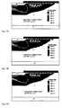
- Fig. 7 illustrates a power device 62 configured to handle high forward and reverse blocking voltages according to one embodiment of the present invention.
- the device 62 is a thyristor like the device 54 and has similar structures. Accordingly, the same numerals are used to denote the corresponding structures in the two devices.
- the device 62 includes an isolation diffusion region 2 that extends from an upper surface 3 to a lower surface 4 of a semiconductor substrate 1.
- the substrate has resistivity of about 77 Ohm-cm (5.57 X 10 13 cm -3 ) and has thickness of about 380 ⁇ m.
- the surface concentration of the isolation diffusion region is formed by diffusing aluminum vertically into the substrate from the upper and lower surfaces of the substrate. Surface concentration of the isolation diffusion region is provided to be about 1 X 10 17 cm -3 .
- the lateral aluminum diffusion is about 0.7 times the aluminum junction depth.
- two or more dopants may be used to form the isolation diffusion region, e.g., use boron to form an upper portion of the isolation region and aluminum to form a lower portion of the isolation region.
- An oxide layer 11 and a polymid layer 12 are provided on the upper surface of the substrate as dual passivation layers to prevent contamination or damage to the device.
- Other dielectric materials may be used, e.g., silicon nitride, diamond-like-carbon, and the like.
- a peripheral junction region 9 is formed inside of the isolation diffusion region proximate the upper surface of the substrate.
- the region 9 is a P+ region and is provided to increase the reverse blocking voltage of the device by reducing the electric field at an upper PN junction of the isolation diffusion region.
- the peripheral junction region 9 is provided to compensate for the surface depletion of aluminum.
- boron is used as the dopant, but other dopants including aluminum may be used.
- the peripheral junction region is provided entirely within the isolation diffusion region. High electric field results if the peripheral region extends outside of the isolation diffusion region.
- the junction depth is about 44 ⁇ m, but may be 35-45 ⁇ m, or 30-50 ⁇ m.
- a first and second conductive regions 5 and 15 are provided on the upper surface and the lower surface, respectively, of the substrate. These regions are P+ regions. They may also be referred to as first and second main junction regions.
- the peripheral junction region 9 and conductive regions 5 and 15 are formed at the same time in the present embodiment using boron as the dopant. Boron concentration for these regions are about 2.8 X 10 15 cm -2 .
- the boron concentration may be varied according to the application. In one embodiment, the boron concentration is about 5E17 cm -3 to 1E19 cm -3 .
- the junction depths are about 44 ⁇ m. The depth may be 35-45 ⁇ m, or 30-50 ⁇ m.
- a cathode 7 is formed on the upper surface, overlying the first main junction region.
- An anode 16 is formed on the lower surface, overlying the second main junction region.
- the anode and cathode are formed from aluminum in the present embodiment.
- a plurality of guard rings of first type 217 are provided on the upper surface of the substrate.
- the guard rings are P regions and are provided to increase the forward blocking voltage of the device.
- the guard rings 217 extend no more than 20 ⁇ m or no more than 15 ⁇ m in one embodiment.
- the rings are configured to have depths of about 7-15 ⁇ m, preferably about 10 ⁇ m.
- a window size of about 9 ⁇ m is used to form the 10 ⁇ m depth guard rings 217.
- Surface concentration of the guard rings 217 is about 1E16 cm -3 to 5E17 cm -3 .
- the plurality of shallow guard rings provide fine tuning and robustness.
- the guard rings may also be referred to as forward blocking guard rings or field limiting rings or shallow junction guard rings.
- a first shallow junction region 218 is formed on the first main junction region 5.
- the first shallow junction region 218 is formed using the same process step as that of the shallow junction guard rings 217. These two structures have similar dopant concentration levels and depths.
- the first shallow junction region includes an outward extension 218a that extends outside of the first main junction 5.
- the region 218 is provided to increase the forward breakdown voltage by pushing equipotential contours to the guard rings 217. Without it, high electric field is generated between the first main junction region 5 and the substrate 1 due the process mismatch between the first main junction 5 and the shallow junction guard rings 217.
- the first shallow junction region 218 is provided to allow alignment tolerance between the deep junction structure (i.e., the first main junction region 5) and the shallow junction region (i.e., the guard rings 217).
- the guard rings 217 has about 1/4 the depth of the first main junction region 5.
- Fig. 9A shows potential contours for the device 62 with the shallow junction region 218 and fixed oxide charge of 1E11 cm -2 .
- Fig. 9B shows a similar device without the shallow junction region 218. The breakdown voltage decreases from 1835 volts to 1685 volts.
- a channel stopper 14 is provided on the upper surface between the guard rings 218 and the isolation diffusion region.
- the channel stopper is an N+ type region and is configured to reduce electricity field at the upper portion of the substrate.
- Surface concentration of the channel stopper is about 1 X 10 20 cm -3 .
- the junction depth of the channel stopper is about 20 ⁇ m.
- a second shallow junction region 220 is formed on the peripheral junction region 9.
- the second shallow junction region 220 has low dopant concentration when compared to the peripheral junction region 9.
- the region 220 has boron concentration of about 1E16-5E17 cm -3 and has depth of about 7-15 ⁇ m, preferably about 10 ⁇ m.
- the region 220 is a P region. In one embodiment, the depth is 20 ⁇ m or less.
- the second shallow junction region 220 is formed at the same time as the guard rings 217 and first shallow junction 218 in the present embodiment.
- the second shallow junction region 220 has an outward extension 220a that extends outside of the isolation diffusion region.
- the low concentration of boron outside of the isolation diffusion region causes a curvature effect at the P/N junction defined by the outward extension 220a and the substrate 1. This increases electric field at that location and causes premature breakdown.
- a plurality of shallow junction guard rings 219 are provided proximate the isolation diffusion region and the outward extension of the second shallow junction region, i.e., between the isolation diffusion region and the channel stopper.
- the guard rings 219 increase the reverse blocking breakdown voltage and are configured to handle the increased electric field generated at the P/N junction defined by the second shallow junction and the substrate.
- the guard rings 219 extend no more than 20 ⁇ m deep in one embodiment, and no more than 15 ⁇ m in another embodiment.
- the rings are configured to have depths of about 7-15 ⁇ m, preferably about 10 ⁇ m.
- a window size of about 9 ⁇ m is used to form the 10 ⁇ m depth guard rings 219.
- Surface concentration of the guard rings is about 1E16 cm -3 to 5E17 cm -3 .
- 10 shallow junction guard rings 219 are used in place of the single guard ring 13 of the device 58.
- the guard rings are spaced apart in such a way to reduce the electric field between the P/N junction and the guard rings 219.
- the guard rings 219 are formed at the same time with the guard rings 218 and the first and second shallow junction regions 218 and 220 in the present embodiment. These structures are formed separately from the first main junction and the peripheral junction region.
- the guard rings 219 may also be referred to as reverse blocking guard rings or field limiting rings or shallow junction guard rings.
- Fig. 8 illustrates a power device 64 according to another embodiment of the invention.
- the power device 64 has a plurality of shallow junction guard rings 219.
- the device 64 has a peripheral junction region 9 and a second shallow junction 220, as in the device 62.
- the device 64 does not includes a channel stopper 14, shallow junction guard rings 218, and first shallow junction region 218 since the device is a diode.
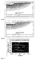
- Fig. 10 illustrates forward breakdown voltage graphs associated with the device 62 having the first shallow junction region 218 and shallow junction guard rings 219.
- a graph 302 shows the effects on the breakdown voltage of the device as the oxide charges increases.
- a graph 304 indicates the effects on the breakdown voltage of a device that, unlike the device 62, does not have the first shallow junction region. Both graphs show only 3-4% degradation in the breakdown voltage as the oxide charge increases. These graphs indicate that the shallow junction region does not significantly affect the forward breakdown voltage.
- the present inventor has also determined that the device 62 is not sensitive to the design or process tolerance from active boron mask to the guard ring structures due to the presence of the shallow junction region. Often times there is some variation, e.g., about 5%, in the junction depth from one process to another. The guard rings, therefore, need to be designed so that such a process variation does not cause serious degradation in the breakdown voltage.
- the process variation includes the differences in the junction depth and oxide charge.
- FIGs. 11A-11C illustrate a simulation performed by the present inventor with respect to the forward blocking voltage on the power device 62 that is provided with a shallow junction region 218 and 10 shallow guard rings 217. It is relatively easier to design a power device with high breakdown voltages and low sensitivity to the process variation since each guard ring share in potential.
Landscapes
- Engineering & Computer Science (AREA)
- Microelectronics & Electronic Packaging (AREA)
- Power Engineering (AREA)
- Physics & Mathematics (AREA)
- Ceramic Engineering (AREA)
- Condensed Matter Physics & Semiconductors (AREA)
- General Physics & Mathematics (AREA)
- Computer Hardware Design (AREA)
- Thyristors (AREA)
- Bipolar Transistors (AREA)
- Electrodes Of Semiconductors (AREA)
- Element Separation (AREA)
Claims (4)
- Leistungsanordnung, mit:- einem n-dotierten Halbleitersubstrat (1) mit einem spezifischen Widerstand von etwa 77 Ωcm, das eine obere Oberfläche (3) und eine untere Oberfläche (4) aufweist, wobei das Halbleitersubstrat (1) eine Dicke von etwa 380 µm aufweist;- einem Kathodenterminal (7), das mit einem p-dotierten ersten leitfähigen Bereich (5) gekoppelt ist, der benachbart der oberen Oberfläche des Substrats bereitgestellt wird, wobei das erste Elektrodenterminal über der oberen Oberfläche des Substrats bereitgestellt wird;- einem Anodenterminal (16), das mit einem p-dotierten zweiten leitfähigen Bereich (15) gekoppelt ist, der benachbart der unteren Oberfläche des Substrats bereitgestellt wird, wobei das zweite Elektrodenterminal unter der unteren Oberfläche des Substrats bereitgestellt wird;- ersten und zweiten p-dotierten leitfähigen Bereichen (5) und (15), die auf der oberen und unteren Oberfläche des Substrats bereitgestellt werden, die eine Borkonzentration zwischen 5 x 1017 cm-3 und 1 x 1019 cm-3 und eine erste Tiefe zwischen 30 µm und 50 µm aufweisen;- einem Isolations-Diffusionsbereich (2) mit einer zweiten Leitfähigkeit, der an einem Umfang des Substrats bereitgestellt wird und sich von der oberen Oberfläche zu der unteren Oberfläche des Substrats erstreckt, wobei der Isolations-Diffusionsbereich eine erste Oberfläche aufweist, die der oberen Oberfläche des Substrats entspricht, und eine zweite Oberfläche aufweist, die der unteren Oberfläche des Substrats entspricht, wobei der Isolations-Diffusionsbereich eine Aluminium-Oberflächenkonzentration von etwa 1 x 1017 cm-3 aufweist;- einem p-dotierten peripheren Übergangsbereich (9), der vollständig innerhalb des Isolations-Diffusionsbereichs ausgebildet ist und benachbart der ersten Oberfläche des Isolations-Diffusionsbereichs ausgebildet ist, wobei der periphere Übergangsbereich (9) eine erste Tiefe und eine Borkonzentration zwischen 5 x 1017 cm-3 und 1 x 1019 cm-3 aufweist;- einer Mehrzahl von p-dotierten flachen Übergangsschutzringen (219, 217) mit einer Oberflächendotierungskonzentration zwischen 1 x 1016 cm-3 und 5 x 1017 cm, die benachbart der oberen Oberfläche des Substrats bereitgestellt werden, wobei die flachen Übergangsschutzringe (219, 217) eine zweite Tiefe von nicht mehr als 20 µm aufweisen;- einem ersten p-dotierten flachen Übergangsbereich (218), der auf dem ersten Hauptübergangsbereich (5) ausgebildet ist, wobei der erste flachen Übergangsbereich (218) eine nach außen gerichtete Erstreckung (218a) aufweist, die sich außerhalb des ersten Hauptübergangsbereichs erstreckt;- einem zweiten p-dotierten flachen Übergangsbereich (220), der den peripheren Übergangsbereich (9) überlagert, wobei der erste flache Übergangsbereich (220) eine nach innen gerichtete Erstreckung (220a) aufweist, die sich außerhalb des Isolations-Diffusionsbereichs erstreckt:- einem Kanalstopper (14) vom erstem Leitfähigkeitstyp, der eine Oberflächenkonzentration von etwa 1 x 1020 cm-3 und eine Tiefe von etwa 20 µm aufweist, wobei der Kanalstopper zwischen dem ersten flachen Übergangsbereich (218) und dem Isolations-Diffusionsbereich (2) bereitgestellt wird; und- einer Oxid- und einer Polyimid-Passivierungsschicht (11, 12), die auf der oberen Oberfläche des Substrats bereitgestellt werden.
- Leistungsanordnung, mit:- einem n-dotierten Halbleitersubstrat (1) mit etwa 77 Ωcm, das eine obere Oberfläche (3) und eine untere Oberfläche (4) aufweist;- einem Kathodenterminal (7), das mit einem n-dotierten ersten leitfähigen Bereich (5) gekoppelt ist, der benachbart der oberen Oberfläche des Substrats bereitgestellt wird, wobei das erste Elektrodenterminal über der oberen Oberfläche des Substrats bereitgestellt wird;- einem Anodenterminal (16), das mit einem p-dotierten zweiten leitfähigen Bereich (15) gekoppelt ist, der benachbart der unteren Oberfläche des Substrats bereitgestellt wird, wobei das zweite Elektrodenterminal unter der unteren Oberfläche des Substrats bereitgestellt wird;- einem ersten p-dotierten leitfähigen Bereich (15), der auf der unteren Oberfläche des Substrats bereitgestellt wird, der eine Borkonzentration zwischen 5 x 1017 cm-3 und 1 x 1019 cm-3 und eine erste Tiefe zwischen 30 µm und 50 µm aufweist;- einem p-dotierten Isolations-Diffusionsbereich (2), der an einem Umfang des Substrats bereitgestellt wird und sich von der oberen Oberfläche zu der unteren Oberfläche des Substrats erstreckt, wobei der Isolations-Diffusionsbereich eine erste Oberfläche aufweist, die der oberen Oberfläche des Substrats entspricht, und eine zweite Oberfläche aufweist, die der unteren Oberfläche des Substrats entspricht, wobei der Isolations-Diffusionsbereich eine Aluminium-Oberflächenkonzentration von etwa 1 x 1017 cm-3 aufweist;- einem p-dotierten peripheren Übergangsbereich (9), der vollständig innerhalb des Isolations-Diffusionsbereichs ausgebildet ist und benachbart der ersten Oberfläche des Isolations-Diffusionsbereichs ausgebildet ist, wobei der periphere Übergangsbereich (9) eine erste Tiefe und eine Borkonzentration zwischen 5 x 1017 cm-3 und 1 x 1019 cm-3 aufweist;- einer Mehrzahl von flachen p-dotierten Übergangsschutzringen (219) mit einer Oberflächendotierungskonzentration zwischen 1 x 1016 cm-3 und 5 x 1017 cm, die benachbart der oberen Oberfläche des Substrats bereitgestellt werden, wobei die flachen Übergangsschutzringe (219) eine zweite Tiefe von nicht mehr als 20 µm aufweisen;- einem ersten p-dotierten flachen Übergangsbereich (220), der den peripheren Übergangsbereich (9) überlagert, wobei der erste flache Übergangsbereich (220) eine nach innen gerichtete Erstreckung (220a) aufweist, die sich außerhalb des Isolations-Diffusionsbereichs erstreckt:- wobei der erste flache Übergangsbereich (220) eine ähnliche Dotierungskonzentration und Diffusionstiefe wie die flachen Übergangsschutzringe (219) aufweist; und- einer Oxid- und einer Polyimid-Passivierungsschicht (11, 12), die auf der oberen Oberfläche des Substrats bereitgestellt werden.
- Anordnung gemäß Anspruch 1, die einen Thyristor bildet.
- Anordnung gemäß Anspruch 2, die eine Diode bildet.
Applications Claiming Priority (2)
| Application Number | Priority Date | Filing Date | Title |
|---|---|---|---|
| US40688102P | 2002-08-28 | 2002-08-28 | |
| US406881P | 2002-08-28 |
Publications (3)
| Publication Number | Publication Date |
|---|---|
| EP1394860A2 EP1394860A2 (de) | 2004-03-03 |
| EP1394860A3 EP1394860A3 (de) | 2005-07-06 |
| EP1394860B1 true EP1394860B1 (de) | 2014-02-26 |
Family
ID=31496014
Family Applications (1)
| Application Number | Title | Priority Date | Filing Date |
|---|---|---|---|
| EP03018788.4A Expired - Lifetime EP1394860B1 (de) | 2002-08-28 | 2003-08-28 | Leistungsanordnungen mit verbesserten Durchbruchsspannungen |
Country Status (2)
| Country | Link |
|---|---|
| US (1) | US8093652B2 (de) |
| EP (1) | EP1394860B1 (de) |
Families Citing this family (24)
| Publication number | Priority date | Publication date | Assignee | Title |
|---|---|---|---|---|
| EP1717863B1 (de) * | 2005-04-28 | 2011-11-02 | Ixys Corporation | Leistungshalbleiteranordnung mit Passivierungsschichten |
| EP1722423B1 (de) * | 2005-05-12 | 2016-07-06 | Ixys Corporation | Stabile Dioden für Niedrig- und Hochfrequenzanwendungen |
| DE102005041838B3 (de) * | 2005-09-02 | 2007-02-01 | Infineon Technologies Ag | Halbleiterbauelement mit platzsparendem Randabschluss und Verfahren zur Herstellung eines solchen Bauelements |
| DE102006011697B4 (de) * | 2006-03-14 | 2012-01-26 | Infineon Technologies Austria Ag | Integrierte Halbleiterbauelementeanordnung und Verfahren zu deren Herstellung |
| DE102010024257B4 (de) * | 2010-06-18 | 2020-04-30 | Semikron Elektronik Gmbh & Co. Kg | Leistungshalbleiterbauelement mit zweistufigem Dotierungsprofil |
| EP2463913A1 (de) * | 2010-12-13 | 2012-06-13 | ABB Technology AG | Bipolares rückwärtssperrendes Non-punch-through-Leistungshalbleiterbauelement |
| JP5739826B2 (ja) * | 2012-01-23 | 2015-06-24 | 株式会社東芝 | 半導体装置 |
| WO2013172059A1 (ja) * | 2012-05-15 | 2013-11-21 | 富士電機株式会社 | 半導体装置 |
| US8836090B1 (en) | 2013-03-01 | 2014-09-16 | Ixys Corporation | Fast recovery switching diode with carrier storage area |
| JP6496992B2 (ja) * | 2014-07-22 | 2019-04-10 | 富士電機株式会社 | 半導体装置 |
| CN104638023B (zh) * | 2015-02-15 | 2017-10-17 | 电子科技大学 | 一种垂直型恒流二极管 |
| EP3142143A1 (de) | 2015-09-11 | 2017-03-15 | ABB Technology AG | Verfahren zur herstellung eines leistungshalbleiterbauelements |
| WO2017076659A1 (en) * | 2015-11-05 | 2017-05-11 | Abb Schweiz Ag | Power semiconductor device and method for producing a power semiconductor device |
| US9590033B1 (en) | 2015-11-20 | 2017-03-07 | Ixys Corporation | Trench separation diffusion for high voltage device |
| US9704832B1 (en) | 2016-02-29 | 2017-07-11 | Ixys Corporation | Die stack assembly using an edge separation structure for connectivity through a die of the stack |
| CN107180763B (zh) * | 2016-03-10 | 2020-03-06 | 北大方正集团有限公司 | 提高vdmos器件击穿电压的方法 |
| CN105552122A (zh) * | 2016-03-14 | 2016-05-04 | 江苏捷捷微电子股份有限公司 | 一种带有深阱终端环结构的平面可控硅芯片及其制造方法 |
| US10193000B1 (en) | 2017-07-31 | 2019-01-29 | Ixys, Llc | Fast recovery inverse diode |
| US10319669B2 (en) | 2017-08-31 | 2019-06-11 | Ixys, Llc | Packaged fast inverse diode component for PFC applications |
| US10424677B2 (en) | 2017-08-31 | 2019-09-24 | Littelfuse, Inc. | Charge carrier extraction inverse diode |
| CN107644905A (zh) * | 2017-10-25 | 2018-01-30 | 启东吉莱电子有限公司 | 一种高压平面闸流管器件及其制作方法 |
| JP7068994B2 (ja) * | 2018-11-26 | 2022-05-17 | 三菱電機株式会社 | 半導体装置 |
| CN110828548A (zh) * | 2019-10-25 | 2020-02-21 | 深圳市德芯半导体技术有限公司 | 一种可控硅器件及其制备方法 |
| JP2023035433A (ja) * | 2021-09-01 | 2023-03-13 | 三菱電機株式会社 | 半導体装置、半導体装置の製造方法、および電力変換装置 |
Family Cites Families (18)
| Publication number | Priority date | Publication date | Assignee | Title |
|---|---|---|---|---|
| JPS5383472A (en) * | 1976-12-28 | 1978-07-22 | Fuji Electric Co Ltd | Semiconductor element |
| US4606781A (en) * | 1984-10-18 | 1986-08-19 | Motorola, Inc. | Method for resistor trimming by metal migration |
| US4972247A (en) * | 1985-10-28 | 1990-11-20 | Silicon Systems, Inc. | High energy event protection for semiconductor devices |
| US5241210A (en) * | 1987-02-26 | 1993-08-31 | Kabushiki Kaisha Toshiba | High breakdown voltage semiconductor device |
| DE3832709A1 (de) | 1988-09-27 | 1990-03-29 | Asea Brown Boveri | Thyristor |
| US5024922A (en) * | 1988-11-07 | 1991-06-18 | Moss Mary G | Positive working polyamic acid/imide and diazoquinone photoresist with high temperature pre-bake |
| JPH02126677A (ja) * | 1988-11-07 | 1990-05-15 | Toshiba Corp | 半導体装置 |
| JP2590284B2 (ja) * | 1990-02-28 | 1997-03-12 | 株式会社日立製作所 | 半導体装置及びその製造方法 |
| US5316964A (en) * | 1991-05-31 | 1994-05-31 | Linear Technology Corporation | Method of forming integrated circuits with diffused resistors in isolation regions |
| KR100243961B1 (ko) | 1991-07-02 | 2000-02-01 | 요트.게.아. 롤페즈 | 반도체장치 |
| JP2812093B2 (ja) * | 1992-09-17 | 1998-10-15 | 株式会社日立製作所 | プレーナ接合を有する半導体装置 |
| US5262754A (en) * | 1992-09-23 | 1993-11-16 | Electromer Corporation | Overvoltage protection element |
| US5698454A (en) * | 1995-07-31 | 1997-12-16 | Ixys Corporation | Method of making a reverse blocking IGBT |
| JP3581447B2 (ja) * | 1995-08-22 | 2004-10-27 | 三菱電機株式会社 | 高耐圧半導体装置 |
| DE19843537C2 (de) | 1998-09-23 | 2000-11-30 | Semikron Elektronik Gmbh | Vierschicht-Halbleiterbauelement als Überspannungsschutz |
| FR2787637B1 (fr) * | 1998-12-18 | 2001-03-09 | Centre Nat Rech Scient | Structure peripherique pour dispositif monolithique de puissance |
| FR2800513B1 (fr) | 1999-11-03 | 2002-03-29 | St Microelectronics Sa | Detecteur d'etat de composant de puissance |
| FR2815471B1 (fr) * | 2000-10-12 | 2003-02-07 | St Microelectronics Sa | Composant vertical a tenue en tension elevee |
-
2003
- 2003-08-27 US US10/650,451 patent/US8093652B2/en not_active Expired - Lifetime
- 2003-08-28 EP EP03018788.4A patent/EP1394860B1/de not_active Expired - Lifetime
Also Published As
| Publication number | Publication date |
|---|---|
| US8093652B2 (en) | 2012-01-10 |
| EP1394860A2 (de) | 2004-03-03 |
| US20040119087A1 (en) | 2004-06-24 |
| EP1394860A3 (de) | 2005-07-06 |
Similar Documents
| Publication | Publication Date | Title |
|---|---|---|
| EP1394860B1 (de) | Leistungsanordnungen mit verbesserten Durchbruchsspannungen | |
| US5629552A (en) | Stable high voltage semiconductor device structure | |
| US9281392B2 (en) | Charge compensation structure and manufacturing therefor | |
| US8704292B2 (en) | Vertical capacitive depletion field effect transistor | |
| TW201306264A (zh) | 半導體功率元件及其製備方法 | |
| EP1722423B1 (de) | Stabile Dioden für Niedrig- und Hochfrequenzanwendungen | |
| US8564059B2 (en) | High-voltage vertical power component | |
| KR20000064647A (ko) | 반도체 디바이스 | |
| CN114512540A (zh) | 用于功率半导体元件的高压终端结构及其制造方法 | |
| WO2012150161A1 (en) | Bipolar junction transistor in silicon carbide with improved breakdown voltage | |
| US6459133B1 (en) | Enhanced flux semiconductor device with mesa and method of manufacturing same | |
| US20220149196A1 (en) | Gate trench power semiconductor devices having improved deep shield connection patterns | |
| US10304971B2 (en) | High speed Schottky rectifier | |
| US8686515B2 (en) | Double-groove bidirectional vertical component | |
| US7253474B2 (en) | Quasi-vertical semiconductor component | |
| US7291899B2 (en) | Power semiconductor component | |
| US10157982B2 (en) | Charge compensation semiconductor devices | |
| CN219017660U (zh) | 高电压半导体器件 | |
| US20240072110A1 (en) | Semiconductor device and manufacturing method of semiconductor device | |
| CN114744035B (zh) | 一种超势垒栅肖特基整流器及其制造方法 | |
| CN216054719U (zh) | 半导体结构 | |
| US11158703B2 (en) | Space efficient high-voltage termination and process for fabricating same | |
| US11810913B2 (en) | Semiconductor device | |
| US20230317797A1 (en) | Wide band gap semiconductor device and manufacturing method | |
| NL2019537B1 (en) | Semiconductor device and method of manufacturing the same |
Legal Events
| Date | Code | Title | Description |
|---|---|---|---|
| PUAI | Public reference made under article 153(3) epc to a published international application that has entered the european phase |
Free format text: ORIGINAL CODE: 0009012 |
|
| AK | Designated contracting states |
Kind code of ref document: A2 Designated state(s): AT BE BG CH CY CZ DE DK EE ES FI FR GB GR HU IE IT LI LU MC NL PT RO SE SI SK TR |
|
| AX | Request for extension of the european patent |
Extension state: AL LT LV MK |
|
| PUAL | Search report despatched |
Free format text: ORIGINAL CODE: 0009013 |
|
| AK | Designated contracting states |
Kind code of ref document: A3 Designated state(s): AT BE BG CH CY CZ DE DK EE ES FI FR GB GR HU IE IT LI LU MC NL PT RO SE SI SK TR |
|
| AX | Request for extension of the european patent |
Extension state: AL LT LV MK |
|
| 17P | Request for examination filed |
Effective date: 20051220 |
|
| AKX | Designation fees paid |
Designated state(s): DE FR IT |
|
| 17Q | First examination report despatched |
Effective date: 20060123 |
|
| RIC1 | Information provided on ipc code assigned before grant |
Ipc: H01L 29/861 20060101ALI20130703BHEP Ipc: H01L 29/06 20060101AFI20130703BHEP Ipc: H01L 29/74 20060101ALI20130703BHEP |
|
| GRAP | Despatch of communication of intention to grant a patent |
Free format text: ORIGINAL CODE: EPIDOSNIGR1 |
|
| INTG | Intention to grant announced |
Effective date: 20130917 |
|
| GRAS | Grant fee paid |
Free format text: ORIGINAL CODE: EPIDOSNIGR3 |
|
| GRAA | (expected) grant |
Free format text: ORIGINAL CODE: 0009210 |
|
| AK | Designated contracting states |
Kind code of ref document: B1 Designated state(s): DE FR IT |
|
| REG | Reference to a national code |
Ref country code: DE Ref legal event code: R096 Ref document number: 60345746 Country of ref document: DE Effective date: 20140410 |
|
| REG | Reference to a national code |
Ref country code: DE Ref legal event code: R082 Ref document number: 60345746 Country of ref document: DE Representative=s name: WINTER, BRANDL, FUERNISS, HUEBNER, ROESS, KAIS, DE |
|
| REG | Reference to a national code |
Ref country code: DE Ref legal event code: R097 Ref document number: 60345746 Country of ref document: DE |
|
| PLBE | No opposition filed within time limit |
Free format text: ORIGINAL CODE: 0009261 |
|
| STAA | Information on the status of an ep patent application or granted ep patent |
Free format text: STATUS: NO OPPOSITION FILED WITHIN TIME LIMIT |
|
| 26N | No opposition filed |
Effective date: 20141127 |
|
| REG | Reference to a national code |
Ref country code: DE Ref legal event code: R097 Ref document number: 60345746 Country of ref document: DE Effective date: 20141127 |
|
| PG25 | Lapsed in a contracting state [announced via postgrant information from national office to epo] |
Ref country code: IT Free format text: LAPSE BECAUSE OF FAILURE TO SUBMIT A TRANSLATION OF THE DESCRIPTION OR TO PAY THE FEE WITHIN THE PRESCRIBED TIME-LIMIT Effective date: 20140226 |
|
| REG | Reference to a national code |
Ref country code: FR Ref legal event code: PLFP Year of fee payment: 13 |
|
| REG | Reference to a national code |
Ref country code: FR Ref legal event code: PLFP Year of fee payment: 14 |
|
| REG | Reference to a national code |
Ref country code: FR Ref legal event code: PLFP Year of fee payment: 15 |
|
| REG | Reference to a national code |
Ref country code: FR Ref legal event code: PLFP Year of fee payment: 16 |
|
| REG | Reference to a national code |
Ref country code: DE Ref legal event code: R082 Ref document number: 60345746 Country of ref document: DE Representative=s name: WINTER, BRANDL, FUERNISS, HUEBNER, ROESS, KAIS, DE Ref country code: DE Ref legal event code: R081 Ref document number: 60345746 Country of ref document: DE Owner name: LITTELFUSE, INC. (N.D.GES.D.STAATES DELAWARE),, US Free format text: FORMER OWNER: IXYS CORP., SANTA CLARA, CALIF., US Ref country code: DE Ref legal event code: R082 Ref document number: 60345746 Country of ref document: DE Representative=s name: WINTER, BRANDL - PARTNERSCHAFT MBB, PATENTANWA, DE |
|
| PGFP | Annual fee paid to national office [announced via postgrant information from national office to epo] |
Ref country code: DE Payment date: 20220608 Year of fee payment: 20 |
|
| PGFP | Annual fee paid to national office [announced via postgrant information from national office to epo] |
Ref country code: FR Payment date: 20220709 Year of fee payment: 20 |
|
| P01 | Opt-out of the competence of the unified patent court (upc) registered |
Effective date: 20230607 |
|
| REG | Reference to a national code |
Ref country code: DE Ref legal event code: R071 Ref document number: 60345746 Country of ref document: DE |