EP1394596B1 - Reflection type liquid crystal display element and liquid crystal display unit - Google Patents
Reflection type liquid crystal display element and liquid crystal display unit Download PDFInfo
- Publication number
- EP1394596B1 EP1394596B1 EP02730903A EP02730903A EP1394596B1 EP 1394596 B1 EP1394596 B1 EP 1394596B1 EP 02730903 A EP02730903 A EP 02730903A EP 02730903 A EP02730903 A EP 02730903A EP 1394596 B1 EP1394596 B1 EP 1394596B1
- Authority
- EP
- European Patent Office
- Prior art keywords
- liquid crystal
- crystal display
- pixel electrode
- display device
- silver
- Prior art date
- Legal status (The legal status is an assumption and is not a legal conclusion. Google has not performed a legal analysis and makes no representation as to the accuracy of the status listed.)
- Expired - Lifetime
Links
Images


Classifications
-
- G—PHYSICS
- G02—OPTICS
- G02F—OPTICAL DEVICES OR ARRANGEMENTS FOR THE CONTROL OF LIGHT BY MODIFICATION OF THE OPTICAL PROPERTIES OF THE MEDIA OF THE ELEMENTS INVOLVED THEREIN; NON-LINEAR OPTICS; FREQUENCY-CHANGING OF LIGHT; OPTICAL LOGIC ELEMENTS; OPTICAL ANALOGUE/DIGITAL CONVERTERS
- G02F1/00—Devices or arrangements for the control of the intensity, colour, phase, polarisation or direction of light arriving from an independent light source, e.g. switching, gating or modulating; Non-linear optics
- G02F1/01—Devices or arrangements for the control of the intensity, colour, phase, polarisation or direction of light arriving from an independent light source, e.g. switching, gating or modulating; Non-linear optics for the control of the intensity, phase, polarisation or colour
- G02F1/13—Devices or arrangements for the control of the intensity, colour, phase, polarisation or direction of light arriving from an independent light source, e.g. switching, gating or modulating; Non-linear optics for the control of the intensity, phase, polarisation or colour based on liquid crystals, e.g. single liquid crystal display cells
- G02F1/133—Constructional arrangements; Operation of liquid crystal cells; Circuit arrangements
- G02F1/1333—Constructional arrangements; Manufacturing methods
- G02F1/1335—Structural association of cells with optical devices, e.g. polarisers or reflectors
-
- G—PHYSICS
- G02—OPTICS
- G02F—OPTICAL DEVICES OR ARRANGEMENTS FOR THE CONTROL OF LIGHT BY MODIFICATION OF THE OPTICAL PROPERTIES OF THE MEDIA OF THE ELEMENTS INVOLVED THEREIN; NON-LINEAR OPTICS; FREQUENCY-CHANGING OF LIGHT; OPTICAL LOGIC ELEMENTS; OPTICAL ANALOGUE/DIGITAL CONVERTERS
- G02F1/00—Devices or arrangements for the control of the intensity, colour, phase, polarisation or direction of light arriving from an independent light source, e.g. switching, gating or modulating; Non-linear optics
- G02F1/01—Devices or arrangements for the control of the intensity, colour, phase, polarisation or direction of light arriving from an independent light source, e.g. switching, gating or modulating; Non-linear optics for the control of the intensity, phase, polarisation or colour
- G02F1/13—Devices or arrangements for the control of the intensity, colour, phase, polarisation or direction of light arriving from an independent light source, e.g. switching, gating or modulating; Non-linear optics for the control of the intensity, phase, polarisation or colour based on liquid crystals, e.g. single liquid crystal display cells
- G02F1/133—Constructional arrangements; Operation of liquid crystal cells; Circuit arrangements
- G02F1/1333—Constructional arrangements; Manufacturing methods
- G02F1/1343—Electrodes
- G02F1/13439—Electrodes characterised by their electrical, optical, physical properties; materials therefor; method of making
-
- G—PHYSICS
- G02—OPTICS
- G02F—OPTICAL DEVICES OR ARRANGEMENTS FOR THE CONTROL OF LIGHT BY MODIFICATION OF THE OPTICAL PROPERTIES OF THE MEDIA OF THE ELEMENTS INVOLVED THEREIN; NON-LINEAR OPTICS; FREQUENCY-CHANGING OF LIGHT; OPTICAL LOGIC ELEMENTS; OPTICAL ANALOGUE/DIGITAL CONVERTERS
- G02F1/00—Devices or arrangements for the control of the intensity, colour, phase, polarisation or direction of light arriving from an independent light source, e.g. switching, gating or modulating; Non-linear optics
- G02F1/01—Devices or arrangements for the control of the intensity, colour, phase, polarisation or direction of light arriving from an independent light source, e.g. switching, gating or modulating; Non-linear optics for the control of the intensity, phase, polarisation or colour
- G02F1/13—Devices or arrangements for the control of the intensity, colour, phase, polarisation or direction of light arriving from an independent light source, e.g. switching, gating or modulating; Non-linear optics for the control of the intensity, phase, polarisation or colour based on liquid crystals, e.g. single liquid crystal display cells
- G02F1/133—Constructional arrangements; Operation of liquid crystal cells; Circuit arrangements
- G02F1/1333—Constructional arrangements; Manufacturing methods
- G02F1/1335—Structural association of cells with optical devices, e.g. polarisers or reflectors
- G02F1/133553—Reflecting elements
-
- G—PHYSICS
- G02—OPTICS
- G02F—OPTICAL DEVICES OR ARRANGEMENTS FOR THE CONTROL OF LIGHT BY MODIFICATION OF THE OPTICAL PROPERTIES OF THE MEDIA OF THE ELEMENTS INVOLVED THEREIN; NON-LINEAR OPTICS; FREQUENCY-CHANGING OF LIGHT; OPTICAL LOGIC ELEMENTS; OPTICAL ANALOGUE/DIGITAL CONVERTERS
- G02F1/00—Devices or arrangements for the control of the intensity, colour, phase, polarisation or direction of light arriving from an independent light source, e.g. switching, gating or modulating; Non-linear optics
- G02F1/01—Devices or arrangements for the control of the intensity, colour, phase, polarisation or direction of light arriving from an independent light source, e.g. switching, gating or modulating; Non-linear optics for the control of the intensity, phase, polarisation or colour
- G02F1/13—Devices or arrangements for the control of the intensity, colour, phase, polarisation or direction of light arriving from an independent light source, e.g. switching, gating or modulating; Non-linear optics for the control of the intensity, phase, polarisation or colour based on liquid crystals, e.g. single liquid crystal display cells
- G02F1/133—Constructional arrangements; Operation of liquid crystal cells; Circuit arrangements
- G02F1/1333—Constructional arrangements; Manufacturing methods
- G02F1/1343—Electrodes
- G02F1/134309—Electrodes characterised by their geometrical arrangement
- G02F1/134336—Matrix
-
- G—PHYSICS
- G02—OPTICS
- G02F—OPTICAL DEVICES OR ARRANGEMENTS FOR THE CONTROL OF LIGHT BY MODIFICATION OF THE OPTICAL PROPERTIES OF THE MEDIA OF THE ELEMENTS INVOLVED THEREIN; NON-LINEAR OPTICS; FREQUENCY-CHANGING OF LIGHT; OPTICAL LOGIC ELEMENTS; OPTICAL ANALOGUE/DIGITAL CONVERTERS
- G02F1/00—Devices or arrangements for the control of the intensity, colour, phase, polarisation or direction of light arriving from an independent light source, e.g. switching, gating or modulating; Non-linear optics
- G02F1/01—Devices or arrangements for the control of the intensity, colour, phase, polarisation or direction of light arriving from an independent light source, e.g. switching, gating or modulating; Non-linear optics for the control of the intensity, phase, polarisation or colour
- G02F1/13—Devices or arrangements for the control of the intensity, colour, phase, polarisation or direction of light arriving from an independent light source, e.g. switching, gating or modulating; Non-linear optics for the control of the intensity, phase, polarisation or colour based on liquid crystals, e.g. single liquid crystal display cells
- G02F1/133—Constructional arrangements; Operation of liquid crystal cells; Circuit arrangements
- G02F1/136—Liquid crystal cells structurally associated with a semi-conducting layer or substrate, e.g. cells forming part of an integrated circuit
- G02F1/1362—Active matrix addressed cells
- G02F1/136277—Active matrix addressed cells formed on a semiconductor substrate, e.g. of silicon
Definitions
- the present invention relates to a reflective liquid crystal display device having a reflective pixel electrode, and a display apparatus using the same such as a reflective liquid crystal projector.
- Liquid crystal display devices have conventionally been used for an image displaying part in various display apparatuses such as a projection display (projector), various portable electric devices, and various information processing terminals, and the like.
- the liquid crystal display device is also called a liquid crystal panel or a liquid crystal cell.
- the kinds of the liquid crystal display device are broadly classified into a transmission type and a reflective type.
- the liquid crystal display devices have a structure in which liquid crystal is enclosed between a pixel electrode substrate and an opposite substrate facing the pixel electrode substrate.
- a transparent electrode made of ITO (Indium Tin Oxide) is located on each of the pixel electrode substrate and the opposite substrate.
- the reflective liquid crystal display device is remarkably expected to provide miniaturization, high fineness, and high efficiency of light-using as a display device, and actually, it is in practical use.
- a transparent electrode made of ITO is located facing the opposite substrate, and a reflective pixel electrode (hereinafter referred to just as “reflective electrode”) is located facing the pixel electrode substrate.
- the reflective liquid crystal display device used for the liquid crystal projector is generally an active type, and an object having C-MOS (Complementary-Metal Oxide Semiconductor) type semiconductor switching circuit formed on a silicon substrate is used as a pixel electrode substrate.
- the reflective electrode is located on the silicon driving-devices substrate.
- the reflective electrode has functions of reflecting light which enters from the side facing the opposite substrate, and of applying voltages to the liquid crystal.
- metallic materials which are generally used in LSI (Large Scale Integrated) processes and contain aluminum (Al) as a principal component, are used.
- the liquid crystal changes its optical properties depending on a potential difference between the opposing electrodes and modulates incident light.
- the optical modulation permits gradation display, and the modulated light is used for displaying images.
- a driving method of reversing polarity to plus or minus for every predetermined period, and applying voltages between the electrodes are generally used in order to prevent ions existing in the liquid crystal from causing burn-in on either of the substrates which is operated.
- Fig. 18 is a schematic diagram showing a driving voltage using the driving method. As expressed by solid line shown in the diagram, if absolute value of each polar voltage applied between the opposing electrodes is the same at V1, it is supposed that there is no difference between actual voltages applied to the liquid crystal, and that the phenomena such as the burn-in as described above does not occur. However, in fact, particularly in the reflective liquid crystal display device, there is a difference between the actual voltages of plus and minus applied to the liquid crystal. This results from different electrode materials which are used respectively for both substrates in the reflective liquid crystal display device.
- ITO is generally used as the transparent electrode as described above, and an aluminum metal film containing slight copper or the like is used as the opposed pixel electrode.
- both electrodes which are respectively made of ITO and aluminum, have different standard electrode potentials from each other, so a battery effect is generated in the device using these electrodes which are made of different metals.
- the standard electrode potential of aluminum is -1.66 V, and combination of the aluminum electrode with the ITO electrode generates a quite high battery effect between these electrodes.
- the driving voltages with both polarities having different absolute values which are obtained by adding DC offset voltage ⁇ V to the driving voltage, should be applied for as expressed by a dashed line in Fig. 18.
- an effective voltage difference between both the polarities being applied to the liquid crystal is 1 V or more, and the difference is applied as the offset voltage ⁇ V.
- the offset voltage ⁇ V is too high, the asymmetry cannot be eliminated completely, and furthermore, the offset voltage ⁇ V is gradually changed from an initial setting value during long term driving, and the internal voltage in the device is stored as a result, so the burn-in occurs. This decreases reliability during the long term driving.
- the offset voltage ⁇ V it is necessary to prepare a circuit for applying it, and an electric circuit system thereof becomes complicated. Therefore, in the reflective liquid crystal display device, battery effect is not preferable, essentially.
- Japanese Patent Laid Open Nos. 9-244068 and 10-54995 teach that metals with a standard electrode potential which is lower enough than that of aluminum, for example, tungsten, (W), titanium (Ti), and titanium nitride (TiN), are used as the reflective electrode material in order to alleviate the above problem of the voltage difference, avoid the battery effect, and reduce the offset voltage.
- US-A-6,081,310 discloses using silver (Ag) as the reflective metal of the pixel electrode.
- the silver comprises an upper layer which is formed on a patterned lower layer comprising one of an electric conductive oxide, Cr, Fe, Ni, Co and Cu.
- a reflective liquid crystal display device according to the preamble of claim 1 is known from WO-A-00/05601 .
- the present invention has been achieved in view of the above problems. It is an object of the invention to provide a reflective liquid crystal display device and a display apparatus which can prevent the battery effect which is a factor of the asymmetry in liquid crystal responses, reduce the offset voltage applied to the driving voltage, and secure high reliability even during the long term driving.
- a reflective liquid crystal display device comprises a pixel electrode substrate which has a reflective pixel electrode made of a metallic material, wherein a principal component of the pixel electrode is aluminum; an opposite substrate which has a transparent electrode being located to face the pixel electrode; and a liquid crystal which a gap between the pixel electrode substrate and the opposite substrate is filled with, wherein the surface of the pixel electrode facing the transparent electrode is covered with a metal film made of a material different from that of the pixel electrode, the material of the metal film having a standard electrode potential with a sign opposite to that of the material of the pixel electrode, characterized in that:
- a display apparatus displays images using light which is modulated by the above reflective liquid crystal display device of the present invention.
- the battery effect between the electrodes is prevented, because the pixel electrode is covered with the metal film which has the standard electrode potential with the sign opposite to that of the metallic material constituting the pixel electrode. This prevents asymmetry in liquid crystal responses and achieves reduction of an offset voltage required for a driving voltage.
- a reflective liquid crystal display device 21 As shown in Fig. 1, a reflective liquid crystal display device 21 according to the embodiment comprises an opposite substrate 30 and a pixel electrode substrate 40 which are located opposite each other, and a liquid crystal layer 35 formed by filling a gap between these substrates is filled with a liquid crystal material.
- the liquid crystal material for forming the liquid crystal layer 35 is a vertical alignment type nematic liquid crystal which is generally called vertically aligned liquid crystal, for example.
- the vertical alignment means a state where molecular orientation in an initial state of the liquid crystal is aligned vertically to each substrate surface. Generally it is called vertically aligned liquid crystal.
- the opposite substrate 30 comprises a glass substrate 31, and is composed of at least a transparent electrode layer 32 and an oriented film 33 which are laminated on a surface of the glass substrate 31 facing the liquid crystal layer 35. Rubbing (orientation) treated films of a polyimide organic compound, and oblique evaporated films such as silicon dioxide (SiO 2 ), are used as the oriented film 33, for example. A surface of the oriented film 33 facing the liquid crystal layer 35 is processed by rubbing treatment so that liquid crystal molecules may be aligned into a predetermined state.
- the transparent electrode layer 32 is constituted by a transparent electrode which has light transmittance and is located on the whole surface.
- ITO which is a solid solution substance of tin oxide (SnO 2 ) and indium oxide (In 2 O 3 ), is used as a material of the transparent electrode.
- a common electric potential for example, an earth potential is applied to all pixel areas of the transparent electrode.
- the pixel electrode substrate 40 comprises a substrate 41 made of a silicon material, for example, and is composed of at least a reflective electrode layer 42, a metal film 43, and an oriented film 44 which are laminated on a surface of the substrate 41 facing the liquid crystal layer 35.
- Switching elements (not shown) for applying voltages selectively to pixel electrodes 42A of the reflective electrode layer 42 are located on the substrate 41.
- polyimide organic compound films and oblique evaporated films such as silicon dioxide are used as the oriented film 44, and a surface thereof is processed by the rubbing treatment.
- the reflective electrode layer 42 is composed of a plurality of the reflective pixel electrodes 42A made of a metallic material which are arranged in a matrix shape.
- the thickness of the reflective electrode layer 42 is 50 nm - 200 nm.
- Aluminum which has high reflectance in the visible region is generally used as a metallic material of the pixel electrodes 42A. More particularly, aluminum metal films containing several wt% or less of copper or silicon which are used for wirings in LSI processes are generally used. Others such as platinum (Pt), silver (Ag), gold (Au), tungsten (W), and titanium (Ti) can be also used as the pixel electrodes 42A.
- a driving voltage is applied to the pixel electrodes 42A by the switching elements which are located on the substrate 41 and which are not illustrated.
- the switching elements are provided respectively corresponding to the pixel electrodes 42A, and are composed of a C-MOS type field effect transistor (FET), for example.
- FET field effect transistor
- the metal film 43 is formed so that surfaces, which face the transparent electrode layer 32, of the pixel electrodes 42A in the reflective electrode layer 42 may be overcoated (covered) on the whole.
- the thickness of the metal film 43 is not less than 1 nm and below 100 nm.
- a dissimilar metallic material which has a standard electrode potential with a sign opposite to that of a metallic material constituting the pixel electrodes 42A, is used as the metal film 43.
- a silver-palladium alloy or a silver-platinum alloy with silver contained therein at a ratio between 20% and 80% in atomic percentage may be used as the metal film 43.
- the pixel electrodes 42A are overcoated with the metal film 43, which is the important feature of the reflective liquid crystal display device 21.
- incident light L1 enters first the opposite substrate 30, passes through the liquid crystal layer 35, and is reflected with a reflective function of the pixel electrodes 42A which are located in the reflective electrode layer 42.
- the light L1 which is reflected on the reflective electrode layer 42, passes through the liquid crystal layer 35 and the opposite substrate 30 in a direction opposite to the incident direction, and exits.
- optical characteristics of the liquid crystal layer 35 changes corresponding to a potential difference between the opposing electrodes, and this modulates the light L1 passing through the liquid crystal layer 35.
- This optical modulation permits gradation display and the modulated light L2 is used for displaying images.
- the driving voltage which reverses ⁇ of its polarity for every predetermined period is applied to the pixel electrodes 42A of the reflective electrode layer 42, for example.
- different electrode materials are used as the opposing electrodes, so corresponding to the polarity, an internal voltage is generated between the electrodes due to the so-called battery effect, and asymmetry is generated in responses of the liquid crystal.
- a direct voltage for compensating it should be separately applied as an offset voltage for the driving. If the offset voltage is increased, it is difficult to completely compensate it, and furthermore, the value thereof is varied or changed during long term driving, which causes problems such as the burn-in.
- the pixel electrodes 42A are overcoated with the metal film 43, which has the standard electrode potential with the sign opposite to that of the metallic material constituting the pixel electrodes 42A, which prevents the battery effect from being generated between the opposing electrodes.
- the metal film 43 which has the standard electrode potential with the sign opposite to that of the metallic material constituting the pixel electrodes 42A, which prevents the battery effect from being generated between the opposing electrodes.
- the aluminum electrodes are covered with a metal having a standard electrode potential with a sign opposite to that of aluminum, such as silver, palladium, platinum, iridium, or gold as the metal film 43 as shown in Fig. 7.
- a metal having a standard electrode potential with a sign opposite to that of aluminum such as silver, palladium, platinum, iridium, or gold as the metal film 43 as shown in Fig. 7.
- the standard electrode potential of aluminum is as high as 1.66 V and its sign is minus.
- all of the standard electrode potentials of silver, palladium, platinum, and the like have plus sign opposite to that of aluminum and exhibit approximately 1 V.
- alloy films thereof also exhibit a plus value of approximately 1 V.
- the standard electrode potential of the ITO transparent electrode, which constitutes the transparent electrode layer 32 is supposed to be approximately +1V, because the battery effect occurs when there is a potential difference between the opposing electrodes.
- the metallic silver-palladium or silver-platinum alloy having 20% to 80% of silver in atomic percentage contained therein which the pixel electrodes 42A are overcoated with has originally the electric potential of approximately +1V which is expected to be almost the same as the electric potential of the ITO transparent electrode, and thus it is thought that no potential difference occurs between the opposing electrodes, so no battery effect is generated.
- the pixel electrodes 42A are covered with the metal film 43 consisting of silver-palladium or silver-platinum alloy having 20% to 80% of silver in atomic percentage contained therein, which has the standard electrode potential with the sign opposite to that of the metallic material constituting the pixel electrodes 42A, so that the battery effect between the opposing electrodes can be prevented unlike the conventional devices which do not have the covering of the metal film 43.
- the asymmetry in the liquid crystal responses can be prevented, so the reduction of the offset voltage applied to the driving voltage can be accomplished. Therefore, applying the offset voltage becomes unnecessary, or the change of the offset voltage can be decreased during the long term driving, and as a result, high reliability can be secured during the long term driving.
- a circuit for applying the offset voltage is simplified or unnecessary.
- the reflective liquid crystal projector shown in Fig. 17 is a so-called 3 panel type one for displaying color images using three liquid crystal light valves 21R, 21B, and 21G respectively for colors of red, blue, and green.
- the reflective liquid crystal projector comprises a light source 11, dichroic mirrors 12 and 13, and a total reflection mirror 14 which are placed along an optical axis 10. Furthermore, the reflective liquid crystal projector comprises polarizing beam splitters 15, 16, and 17, a combining prism 18, a projector lens 19, and a screen 20.
- the light source 11 emits white light containing red light (R), blue light (G), and green light (B) which are needed for displaying the color images, and is composed of a halogen lamp, a metal halide lamp, or a xenon lamp, for example.
- the dichroic mirror 12 has a function of separating light, which comes from the light source 11, into blue light and light containing other colors.
- the dichroic mirror 13 has a function of separating light, which passes through the dichroic mirror 12, into red light and green light.
- the total reflection mirror 14 reflects the blue light separated by the dichroic mirror 12 toward the polarizing beam splitter 17.
- the polarizing beam splitters 15, 16, and 17 are located along optical paths of red light, green light, and blue light, respectively. These polarizing beam splitters 15, 16, and 17 have surfaces for separating polarized light 15A, 16A, and 17A, respectively, and have a function of separating the incident color light into two polarized light components which are orthogonal mutually in these surfaces for separating polarized light 15A, 16A, and 17A.
- the surfaces for separating polarized light 15A, 16A, and 17A reflect one polarized light component (for example, an S-polarized light component), and transmit the other polarized light component (for example, a P-polarized light component).
- the liquid crystal light valves 21R, 21G, and 21B are composed of the reflective liquid crystal display device 21. These liquid crystal light valves 21R, 21G, and 21B receive color lights of a predetermined polarized light component (for example, the S-polarized light component) separated by the surfaces for separating polarized light 15A, 16A, and 17A of the polarizing beam splitters 15, 16, and 17, respectively.
- the liquid crystal light valves 21R, 21G, and 21B have a function of being driven corresponding to the driving voltage which is applied based on image signals, modulating the incident light, and reflecting the modulated incident light toward the polarizing beam splitters 15, 16, and 17.
- the combining prism 18 has a function of combining the color lights of the predetermined polarized light components (for example, the P-polarized light component) which are emitted from the liquid crystal light valves 21R, 21G, and 21B, and pass through the polarizing beam splitters 15, 16, and 17.
- the projector lens 19 has a function of projecting the combined light, which is emitted from the combining prism 18, toward the screen 20.
- the white light emitted from the light source 11 is first separated into the blue light and the light containing other colors (the red light and the green light) with the function of the dichroic mirror 12.
- the blue light is reflected towards the polarizing beam splitter 17 with the function of the total reflection mirror 14.
- the red light and the green light are further separated into the red light and the green light with the function of the dichroic mirror 13.
- the separated red light and green light enter the polarizing beam splitters 15 and 16, respectively.
- Each of the polarizing beam splitters 15, 16, and 17 separates the incident color light into the two polarized light components, which are orthogonal each other, in the surfaces for separating polarized light 15A, 16A, and 17A.
- the surfaces for separating polarized light 15A, 16A, and 17A reflect one of the polarized light components (for example, the S-polarized light component) toward the liquid crystal light valves 21R, 21G, and 21B.
- the liquid crystal light valves 21R, 21G, and 21B are driven corresponding to the driving voltage, which is applied based on the image signals, to modulate the color light of the incident predetermined polarized light component per pixel.
- the liquid crystal light valves 21R, 21G, and 21B are composed of the above reflective liquid crystal display device 21, so the offset voltage is reduced and they are driven by the driving voltage having more excellent symmetry compared with the conventional types.
- the liquid crystal light valves 21R, 21G, and 21B reflect the modulated color light to the polarizing beam splitters 15, 16, and 17.
- the polarizing beam splitters 15, 16, and 17 transmit only the predetermined polarized light component (for example, the P-polarized light component) of the reflected light (the modulated light) which is from the liquid crystal light valves 21R, 21G, and 21B, and emit the component towards the combining prism 18.
- the combining prism 18 combines the color lights of the predetermined polarized light components passing through the polarizing beam splitters 15, 16, and 17, and emits the combined light towards the projector lens 19.
- the projector lens 19 projects the combined light, which is emitted from the combining prism 18, toward the screen 20. Thereby, images corresponding to the light modulated by the liquid crystal light valves 21R, 21G, and 21B are projected on the screen 20, which accomplished desired image display.
- the reflective liquid crystal display device 21, in which the pixel electrodes 42A are overcoated with the metal film 43, is used as the liquid crystal light valves 21R, 21G, and 21B, so the offset voltage, which has conventionally been needed for the driving voltage in the liquid crystal light valves 21R, 21G, and 21B, is reduced or unnecessary.
- the circuit for applying the offset voltage is simplified or unnecessary, which allows the driving circuit of the liquid crystal light valves 21R, 21G, and 21B to be simplified.
- Devices were prepared as a reflective liquid crystal display device (a liquid crystal cell) for evaluation which is used as Comparative Example, using ITO as the transparent electrode material in the opposite substrate, and using various metal electrode materials (aluminum, platinum, and the like) as the pixel electrode in the pixel electrode substrate.
- These devices for evaluation were produced as follows. First, a glass substrate having the ITO transparent electrode thereon for using as the opposite substrate, and a silicon substrate having the electrode thereon which is made of one of the various electrodes for using as the pixel electrode substrate were cleaned and introduced into an evaporation apparatus, and a SiO 2 film as the oriented film was formed with oblique evaporation in an evaporation angle range of 45° to 55°. The thickness of the oriented film was 50 nm.
- the pretilt angle of liquid crystal was controlled to become about 3°. Then, a suitable number of glass beads with a diameter of 2 ⁇ m were dispersed between the substrates with the oriented films formed to bond both of the substrates, and a vertical liquid crystal material with negative dielectric anisotropy ⁇ was injected thereinto to produce a reflective liquid crystal cell.
- R(+) and R(-) express reflectances of the device when applying the plus and minus voltages to the side of the pixel electrode, respectively.
- V-T characteristic which is called a V-T characteristic, hereinafter.
- the horizontal axis represents applied voltages (V) and the vertical axis represents reflectance (%).
- the horizontal axis represents absolute values of the applied voltage to simplify the figure.
- the measured values of the reflectance R(-) obtained when using the minus applied voltage were plotted and indicated by circles, and the measured values of the reflectance R(+) obtained when using the plus applied voltage were plotted and indicated by black circles.
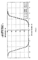
- Fig. 2 shows the V-T characteristic when using aluminum (150 nm in thickness) as the metallic material of the pixel electrode.
- the V-T curves when applying both polarities of the voltages were asymmetric, and the V-T curve of the reflectance when applying the plus voltage R(+) was shifted to a voltage side lower than the V-T curve of the reflectance in the case of the minus R(-). That is, comparing the reflectance at the same magnitude of the applied voltages reveals that a characteristic of R(+) > R(-) was always obtained.
- the liquid crystal was asymmetrically driven in this way in spite of applying the same magnitude of the plus and minus external voltages to the liquid crystal cell, which means that no symmetrical voltage was applied to the liquid crystal.
- This results from the direct current battery effect generated between the dissimilar electrodes of the ITO transparent electrode and the aluminum electrode. If the driving is continued in this state, the internal voltage is stored in the liquid crystal cell, and this causes the burn-in. Therefore, for practical use, the offset voltage ⁇ V equal to the shifted voltage (voltage corresponding to the battery effect) should be applied so as to obtain R(+) R(-).
- the above burn-in phenomenon may occur during the long term driving, unless the value of the ⁇ V is correctly set and continuously applied, and furthermore, the ⁇ V itself may be changed due to the long term driving, change of environmental temperatures, and the like, so reducing or eliminating the ⁇ V is essentially indispensable for practical use.
- Fig. 3 shows the V-T characteristic when using platinum (100 nm in thickness) as the metallic material of the pixel electrode.
- platinum 100 nm in thickness
- Fig. 4 shows the V-T characteristic when using silver (100 nm in thickness) as the metallic material of the pixel electrode.
- a characteristic of R(+) ⁇ R(-) was always obtained like Comparative Example 2.
- Fig. 5 shows the V-T characteristic when using gold (190 nm in thickness) as the metallic material of the pixel electrode.
- gold 190 nm in thickness
- Fig. 6 shows a spectral characteristic of the reflectance when a 60 Hz square wave was applied as the driving voltage to the devices of Comparative Examples 1 to 4.
- the horizontal axis represents wavelength (nm) and the vertical axis represents reflectance (%).
- a plotted curve with black circles represents measurement results when platinum (100 nm in thickness) is used as the metallic material of the pixel electrode (Comparative Example 2), and plotted cures with inverted triangles and circles represent measurement results respectively when using silver (100 nm in thickness) (Comparative Example 3), and gold (190 nm in thickness) (Comparative Example 4).
- a solid line with no plotting point represents measurement results when using aluminum (150 nm in thickness) (Comparative Example 1).
- the measurement was performed with an intensified multichannel spectrophotometer IMUC7000 manufactured by Otsuka Electronics Co., Ltd. using a standard aluminum reflective film as a reference.
- the reflectance on the short wavelength side was decreased remarkably, especially when gold was used as the pixel electrode. Therefore, comparison of only the V-T curves reveals that the utilization of gold as the pixel electrode (Fig. 5) provided substantially no asymmetry and an almost ideal state, but the reflective function was insufficiently obtained as shown in the spectral characteristic of Fig. 6, so gold is a practically unsuitable material.
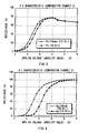
- Fig. 8 shows the V-T characteristic when the aluminum pixel electrodes are overcoated with platinum of 2 nm in thickness as the metal film 43.
- Fig. 8 exhibits R(+) ⁇ R(-) and little asymmetry in the both polarities of the reflectances R(+) and R(-) was observed because of only 2 nm overcoating.
- the offset voltage was 0.5 V and decreased more dramatically than ever before.
- Fig. 9 shows the V-T characteristic when the aluminum pixel electrodes are overcoated with silver of 5 nm in thickness as the metal film 43.
- R(+) R(-) was observed and the asymmetry in both polarities of the reflectances R(+) and R(-) was not observed at all. No offset voltage was observed.
- Fig. 10 shows the V-T characteristic when the aluminum pixel electrodes are overcoated with gold of 5 nm in thickness as the metal film 43.
- R(+) R(-) was observed and the asymmetry in both polarities of the reflectances R(+) and R(-) was not observed substantially. Little offset voltage was observed.
- Fig. 11 shows the V-T characteristic when the aluminum pixel electrodes are overcoated with palladium of 5 nm in thickness as the metal film 43.
- R(+) R(-) was observed and the asymmetry in both polarities of the reflectances R(+) and R(-) was not observed at all. No offset voltage was observed.
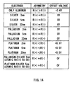
- Fig. 13 shows the measurement results, the vertical axis represents reflectance (%), and the horizontal axis represents the mixture concentrations of silver in each alloy.
- the alloy films of palladium-silver and platinum-silver are effective as a procedure of solving both of the problems of the chemical instability of silver and the low reflectances of palladium and platinum. That is, the chemical instability of silver is eliminated by mixing palladium or platinum which is chemically very stable. Moreover, the reflectance, which is low due to the overcoating of palladium or platinum, is increased even to a value equivalent to that of the original aluminum pixel electrode by mixing silver therewith.
- the mixing ratio which satisfies both characteristics of the chemical stability and the reflectance was an atomic ratio of 20% to 80%, and preferably 40% to 60%.
- Example 2 the V-T characteristic when using the metal film 43 with various thicknesses for overcoating was examined.
- Production of devices for evaluation and measurement conditions are the same as those of Example 1.
- Silver, palladium, and platinum were used as the material of the metal film 43. Only the alloys with silver are according to the claimed invention.
- Fig. 14 shows the measurement results thereof, that is, the relation (an asymmetric situation) between the reflectances R(+) and R(-) and the offset voltage in each of the materials and the thickness. Also, Fig. 14 shows the characteristics when not using the metal film 43 (that is, only the aluminum electrode) for overcoating, and when using the palladium-silver alloy film and the platinum-silver alloy film like Example 2, as well as silver, palladium, and platinum for overcoating.
- the metal film 43 that is, only the aluminum electrode
- the overcoating of the metal film 43 which is made of each material with each thickness reduces the asymmetry and the offset voltage, unlike the case of using only aluminum as the electrode material.
- the thickness less than 1 nm is considered to be also effective for preventing the asymmetry, but it is difficult to uniformly form such a thin film.
- the metal film 43 of 100 nm or more in thickness for overcoating is too thick to transmit light, and to exhibit the original absolute reflectance of the reflective electrode (the pixel electrodes 42A). Therefore, the thickness of the metal film for overcoating is appropriately not less than 1 nm and below 100 nm.
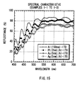
- Fig. 15 A spectral characteristic of the reflectance when applying a 60 Hz square wave as the driving voltage to the devices having the platinum, gold, and silver overcoatings produced in comparative Examples 1-1 to 1-3 (not embodying the invention) was measured (Fig. 15).
- the measurements were performed with the intensified multichannel spectrophotometer IMUC7000 manufactured by Otsuka Electronics Co., Ltd. like Comparative Examples (Fig. 6).
- the horizontal axis represents wavelength (nm) and the vertical axis represents reflectance (%).
- a plotted curve with black circles represents the measurement results when using platinum (2 nm in thickness) as the metal film 43 for overcoating
- plotted curves with circles and inverted triangles represent the measurement results respectively when using gold (5 nm in thickness), and silver (5 nm in thickness) for overcoating
- a solid line with no plotting point represents the measurement results when not using the metal film 43 (the case of the only aluminum electrode) for overcoating as a reference.
- a plotted curve with black circles represents the measurement results when using platinum with a thickness of 2 nm
- plotted curves with circles and rhombus represent the measurement results respectively when using one with a thickness of 5 nm, and a thickness of 20 nm
- a solid line with no plotting point represents the measurement results when not using the metal film 43 (the case of the only aluminum electrode) for overcoating as a reference.
- the reflective liquid crystal display device of the invention can be widely applied not only to the LCD projectors but also to other display apparatuses and image display in various portable electric devices and in various information processing terminals, and the like.
- the surface of the pixel electrode facing the transparent electrode is covered with the metal film, which has the standard electrode potential with the sign opposite to that of the metallic material constituting the pixel electrode, so the battery effect between the opposing electrodes can be prevented.
- the asymmetry of the liquid crystal responses can be prevented, which accomplishes the reduction of the offset voltage which is applied to the driving voltage. Therefore, applying the offset voltage becomes unnecessary, or the change of the offset voltage can be decreased even during the long term driving, and as a result, high reliability can be secured even during the long term driving.
Landscapes
- Physics & Mathematics (AREA)
- Nonlinear Science (AREA)
- Mathematical Physics (AREA)
- Chemical & Material Sciences (AREA)
- Crystallography & Structural Chemistry (AREA)
- General Physics & Mathematics (AREA)
- Optics & Photonics (AREA)
- Geometry (AREA)
- Liquid Crystal (AREA)
- Projection Apparatus (AREA)
Applications Claiming Priority (5)
| Application Number | Priority Date | Filing Date | Title |
|---|---|---|---|
| JP2001169721 | 2001-06-05 | ||
| JP2001169721 | 2001-06-05 | ||
| JP2002135898A JP4010007B2 (ja) | 2001-06-05 | 2002-05-10 | 反射型液晶表示素子および液晶表示装置 |
| JP2002135898 | 2002-05-10 | ||
| PCT/JP2002/005488 WO2002099522A1 (fr) | 2001-06-05 | 2002-06-04 | Element d'affichage a cristaux liquides reflechissants et unite d'affichage a cristaux liquides |
Publications (3)
| Publication Number | Publication Date |
|---|---|
| EP1394596A1 EP1394596A1 (en) | 2004-03-03 |
| EP1394596A4 EP1394596A4 (en) | 2005-07-27 |
| EP1394596B1 true EP1394596B1 (en) | 2008-01-02 |
Family
ID=26616368
Family Applications (1)
| Application Number | Title | Priority Date | Filing Date |
|---|---|---|---|
| EP02730903A Expired - Lifetime EP1394596B1 (en) | 2001-06-05 | 2002-06-04 | Reflection type liquid crystal display element and liquid crystal display unit |
Country Status (7)
| Country | Link |
|---|---|
| US (1) | US6917403B2 (https=) |
| EP (1) | EP1394596B1 (https=) |
| JP (1) | JP4010007B2 (https=) |
| KR (1) | KR100872858B1 (https=) |
| CN (1) | CN1244009C (https=) |
| DE (1) | DE60224386T2 (https=) |
| WO (1) | WO2002099522A1 (https=) |
Families Citing this family (8)
| Publication number | Priority date | Publication date | Assignee | Title |
|---|---|---|---|---|
| US20040165128A1 (en) * | 2003-02-26 | 2004-08-26 | Three-Five Systems, Inc. | Vertically aligned nematic mode liquid crystal display having large tilt angles and high contrast |
| JP3608562B2 (ja) | 2003-03-07 | 2005-01-12 | ソニー株式会社 | 反射型液晶表示素子および液晶表示装置 |
| JP2006171344A (ja) * | 2004-12-15 | 2006-06-29 | Nippon Sheet Glass Co Ltd | 光学膜 |
| JP2006330527A (ja) * | 2005-05-30 | 2006-12-07 | Victor Co Of Japan Ltd | 液晶表示装置及びその製造方法 |
| KR100829743B1 (ko) * | 2005-12-09 | 2008-05-15 | 삼성에스디아이 주식회사 | 유기 박막 트랜지스터 및 이의 제조 방법, 이를 구비한평판 디스플레이 장치 |
| JP2008014965A (ja) * | 2006-06-30 | 2008-01-24 | Mitsubishi Electric Corp | 液晶表示装置 |
| JP5402511B2 (ja) * | 2009-10-19 | 2014-01-29 | セイコーエプソン株式会社 | 液晶装置及びその製造方法、並びに電子機器 |
| CN114167651B (zh) * | 2021-12-10 | 2023-10-31 | Tcl华星光电技术有限公司 | 液晶显示面板 |
Citations (1)
| Publication number | Priority date | Publication date | Assignee | Title |
|---|---|---|---|---|
| WO2000005601A2 (en) * | 1998-07-22 | 2000-02-03 | Koninklijke Philips Electronics N.V. | Display device |
Family Cites Families (10)
| Publication number | Priority date | Publication date | Assignee | Title |
|---|---|---|---|---|
| US4499521A (en) * | 1982-09-13 | 1985-02-12 | North American Philips Corporation | Low-fire ceramic dielectric compositions for multilayer ceramic capacitors |
| JP3117588B2 (ja) * | 1993-08-27 | 2000-12-18 | シャープ株式会社 | 液晶表示用反射板 |
| JPH085806A (ja) * | 1994-06-17 | 1996-01-12 | Mitsui Toatsu Chem Inc | 反射体およびそれを用いた液晶表示用バックライトランプリフレクター |
| JPH09244068A (ja) * | 1996-03-06 | 1997-09-19 | Pioneer Electron Corp | 反射型液晶表示装置 |
| JPH1054995A (ja) * | 1996-06-06 | 1998-02-24 | Pioneer Electron Corp | 反射型液晶表示装置 |
| JPH1010569A (ja) * | 1996-06-24 | 1998-01-16 | Pioneer Electron Corp | 反射型液晶表示装置 |
| US6791640B1 (en) * | 1997-04-23 | 2004-09-14 | Sharp Kabushiki Kaisha | Reflection liquid crystal display and reflection liquid crystal display provided with built-in touch panel and comprising the same |
| JP3199312B2 (ja) * | 1997-11-06 | 2001-08-20 | キヤノン株式会社 | 液晶表示装置 |
| JP3410667B2 (ja) | 1997-11-25 | 2003-05-26 | シャープ株式会社 | 反射型液晶表示装置およびその製造方法 |
| JP3520417B2 (ja) * | 2000-12-14 | 2004-04-19 | セイコーエプソン株式会社 | 電気光学パネルおよび電子機器 |
-
2002
- 2002-05-10 JP JP2002135898A patent/JP4010007B2/ja not_active Expired - Fee Related
- 2002-06-04 CN CNB028019598A patent/CN1244009C/zh not_active Expired - Fee Related
- 2002-06-04 US US10/333,549 patent/US6917403B2/en not_active Expired - Fee Related
- 2002-06-04 EP EP02730903A patent/EP1394596B1/en not_active Expired - Lifetime
- 2002-06-04 DE DE60224386T patent/DE60224386T2/de not_active Expired - Fee Related
- 2002-06-04 WO PCT/JP2002/005488 patent/WO2002099522A1/ja not_active Ceased
- 2002-06-04 KR KR1020037000192A patent/KR100872858B1/ko not_active Expired - Fee Related
Patent Citations (1)
| Publication number | Priority date | Publication date | Assignee | Title |
|---|---|---|---|---|
| WO2000005601A2 (en) * | 1998-07-22 | 2000-02-03 | Koninklijke Philips Electronics N.V. | Display device |
Also Published As
| Publication number | Publication date |
|---|---|
| JP4010007B2 (ja) | 2007-11-21 |
| US20040032551A1 (en) | 2004-02-19 |
| DE60224386T2 (de) | 2009-01-02 |
| KR100872858B1 (ko) | 2008-12-10 |
| WO2002099522A1 (fr) | 2002-12-12 |
| US6917403B2 (en) | 2005-07-12 |
| EP1394596A4 (en) | 2005-07-27 |
| CN1244009C (zh) | 2006-03-01 |
| CN1463381A (zh) | 2003-12-24 |
| EP1394596A1 (en) | 2004-03-03 |
| KR20030029612A (ko) | 2003-04-14 |
| JP2003057674A (ja) | 2003-02-26 |
| DE60224386D1 (de) | 2008-02-14 |
Similar Documents
| Publication | Publication Date | Title |
|---|---|---|
| EP1515182B1 (en) | Reflective liquid crystal display device and method of manufacturing the same | |
| JP3380482B2 (ja) | 液晶表示装置 | |
| EP1533650B1 (en) | Liquid crystal display element, and liquid crystal display device | |
| EP1223459B1 (en) | Liquid-crystal display | |
| US6373541B1 (en) | Reflection type liquid crystal display element | |
| EP1394596B1 (en) | Reflection type liquid crystal display element and liquid crystal display unit | |
| US6067142A (en) | Vertically aligned pi-cell LCD having on-state with mid-plane molecules perpendicular to the substrates | |
| EP1513004A1 (en) | Reflective liquid crystal display device, method of manufacturing the same, and liquid crystal display unit | |
| US6271905B1 (en) | Reflective liquid crystal display device | |
| US7362388B2 (en) | Liquid crystal display device, and optical block | |
| EP1602965B1 (en) | Reflection type liquid crystal display element and liquid crystal display unit | |
| US6292238B1 (en) | Reflection-type liquid crystal apparatus | |
| US8194196B2 (en) | Liquid crystal display device using a magnetic driving field and driving method thereof | |
| JP2004012794A (ja) | 反射型液晶表示素子および液晶表示装置 | |
| KR101408411B1 (ko) | 액정 표시 소자 및 투사형 액정 표시 장치 | |
| JP2004012795A (ja) | 反射型液晶表示素子および液晶表示装置 | |
| JP2000056315A (ja) | 液晶表示素子 | |
| KR20000071651A (ko) | 액정 표시 소자 및 이를 이용한 액정 표시 장치 | |
| JP2004038004A (ja) | 反射型液晶表示素子および液晶表示装置 | |
| JP2006184928A (ja) | 液晶装置 |
Legal Events
| Date | Code | Title | Description |
|---|---|---|---|
| PUAI | Public reference made under article 153(3) epc to a published international application that has entered the european phase |
Free format text: ORIGINAL CODE: 0009012 |
|
| 17P | Request for examination filed |
Effective date: 20030114 |
|
| AK | Designated contracting states |
Kind code of ref document: A1 Designated state(s): AT BE CH CY DE DK ES FI FR GB GR IE IT LI LU MC NL PT SE TR |
|
| AX | Request for extension of the european patent |
Extension state: AL LT LV MK RO SI |
|
| A4 | Supplementary search report drawn up and despatched |
Effective date: 20050614 |
|
| RIC1 | Information provided on ipc code assigned before grant |
Ipc: 7G 02F 1/1335 B Ipc: 7G 02F 1/1343 A |
|
| GRAP | Despatch of communication of intention to grant a patent |
Free format text: ORIGINAL CODE: EPIDOSNIGR1 |
|
| GRAJ | Information related to disapproval of communication of intention to grant by the applicant or resumption of examination proceedings by the epo deleted |
Free format text: ORIGINAL CODE: EPIDOSDIGR1 |
|
| 17Q | First examination report despatched |
Effective date: 20051005 |
|
| 17Q | First examination report despatched |
Effective date: 20051005 |
|
| GRAP | Despatch of communication of intention to grant a patent |
Free format text: ORIGINAL CODE: EPIDOSNIGR1 |
|
| GRAS | Grant fee paid |
Free format text: ORIGINAL CODE: EPIDOSNIGR3 |
|
| GRAA | (expected) grant |
Free format text: ORIGINAL CODE: 0009210 |
|
| AK | Designated contracting states |
Kind code of ref document: B1 Designated state(s): DE FR GB |
|
| REG | Reference to a national code |
Ref country code: GB Ref legal event code: FG4D |
|
| REF | Corresponds to: |
Ref document number: 60224386 Country of ref document: DE Date of ref document: 20080214 Kind code of ref document: P |
|
| ET | Fr: translation filed | ||
| PGFP | Annual fee paid to national office [announced via postgrant information from national office to epo] |
Ref country code: DE Payment date: 20080612 Year of fee payment: 7 |
|
| PLBE | No opposition filed within time limit |
Free format text: ORIGINAL CODE: 0009261 |
|
| STAA | Information on the status of an ep patent application or granted ep patent |
Free format text: STATUS: NO OPPOSITION FILED WITHIN TIME LIMIT |
|
| PGFP | Annual fee paid to national office [announced via postgrant information from national office to epo] |
Ref country code: FR Payment date: 20080617 Year of fee payment: 7 |
|
| 26N | No opposition filed |
Effective date: 20081003 |
|
| PGFP | Annual fee paid to national office [announced via postgrant information from national office to epo] |
Ref country code: GB Payment date: 20080604 Year of fee payment: 7 |
|
| GBPC | Gb: european patent ceased through non-payment of renewal fee |
Effective date: 20090604 |
|
| REG | Reference to a national code |
Ref country code: FR Ref legal event code: ST Effective date: 20100226 |
|
| PG25 | Lapsed in a contracting state [announced via postgrant information from national office to epo] |
Ref country code: FR Free format text: LAPSE BECAUSE OF NON-PAYMENT OF DUE FEES Effective date: 20090630 |
|
| PG25 | Lapsed in a contracting state [announced via postgrant information from national office to epo] |
Ref country code: GB Free format text: LAPSE BECAUSE OF NON-PAYMENT OF DUE FEES Effective date: 20090604 |
|
| PG25 | Lapsed in a contracting state [announced via postgrant information from national office to epo] |
Ref country code: DE Free format text: LAPSE BECAUSE OF NON-PAYMENT OF DUE FEES Effective date: 20100101 |