EP1382011B1 - Abdeckung mit radiofrequenzidentifikationsgerät - Google Patents
Abdeckung mit radiofrequenzidentifikationsgerät Download PDFInfo
- Publication number
- EP1382011B1 EP1382011B1 EP02727693A EP02727693A EP1382011B1 EP 1382011 B1 EP1382011 B1 EP 1382011B1 EP 02727693 A EP02727693 A EP 02727693A EP 02727693 A EP02727693 A EP 02727693A EP 1382011 B1 EP1382011 B1 EP 1382011B1
- Authority
- EP
- European Patent Office
- Prior art keywords
- sheet
- chip
- fact
- thickness
- identification device
- Prior art date
- Legal status (The legal status is an assumption and is not a legal conclusion. Google has not performed a legal analysis and makes no representation as to the accuracy of the status listed.)
- Revoked
Links
Images

Classifications
-
- G—PHYSICS
- G06—COMPUTING OR CALCULATING; COUNTING
- G06K—GRAPHICAL DATA READING; PRESENTATION OF DATA; RECORD CARRIERS; HANDLING RECORD CARRIERS
- G06K19/00—Record carriers for use with machines and with at least a part designed to carry digital markings
- G06K19/06—Record carriers for use with machines and with at least a part designed to carry digital markings characterised by the kind of the digital marking, e.g. shape, nature, code
- G06K19/067—Record carriers with conductive marks, printed circuits or semiconductor circuit elements, e.g. credit or identity cards also with resonating or responding marks without active components
- G06K19/07—Record carriers with conductive marks, printed circuits or semiconductor circuit elements, e.g. credit or identity cards also with resonating or responding marks without active components with integrated circuit chips
- G06K19/077—Constructional details, e.g. mounting of circuits in the carrier
- G06K19/07749—Constructional details, e.g. mounting of circuits in the carrier the record carrier being capable of non-contact communication, e.g. constructional details of the antenna of a non-contact smart card
- G06K19/07758—Constructional details, e.g. mounting of circuits in the carrier the record carrier being capable of non-contact communication, e.g. constructional details of the antenna of a non-contact smart card arrangements for adhering the record carrier to further objects or living beings, functioning as an identification tag
-
- G—PHYSICS
- G06—COMPUTING OR CALCULATING; COUNTING
- G06K—GRAPHICAL DATA READING; PRESENTATION OF DATA; RECORD CARRIERS; HANDLING RECORD CARRIERS
- G06K19/00—Record carriers for use with machines and with at least a part designed to carry digital markings
- G06K19/02—Record carriers for use with machines and with at least a part designed to carry digital markings characterised by the selection of materials, e.g. to avoid wear during transport through the machine
- G06K19/025—Record carriers for use with machines and with at least a part designed to carry digital markings characterised by the selection of materials, e.g. to avoid wear during transport through the machine the material being flexible or adapted for folding, e.g. paper or paper-like materials used in luggage labels, identification tags, forms or identification documents carrying RFIDs
-
- G—PHYSICS
- G06—COMPUTING OR CALCULATING; COUNTING
- G06K—GRAPHICAL DATA READING; PRESENTATION OF DATA; RECORD CARRIERS; HANDLING RECORD CARRIERS
- G06K19/00—Record carriers for use with machines and with at least a part designed to carry digital markings
- G06K19/02—Record carriers for use with machines and with at least a part designed to carry digital markings characterised by the selection of materials, e.g. to avoid wear during transport through the machine
- G06K19/027—Record carriers for use with machines and with at least a part designed to carry digital markings characterised by the selection of materials, e.g. to avoid wear during transport through the machine the material being suitable for use as a textile, e.g. woven-based RFID-like labels designed for attachment to laundry items
-
- G—PHYSICS
- G06—COMPUTING OR CALCULATING; COUNTING
- G06K—GRAPHICAL DATA READING; PRESENTATION OF DATA; RECORD CARRIERS; HANDLING RECORD CARRIERS
- G06K19/00—Record carriers for use with machines and with at least a part designed to carry digital markings
- G06K19/06—Record carriers for use with machines and with at least a part designed to carry digital markings characterised by the kind of the digital marking, e.g. shape, nature, code
- G06K19/067—Record carriers with conductive marks, printed circuits or semiconductor circuit elements, e.g. credit or identity cards also with resonating or responding marks without active components
- G06K19/07—Record carriers with conductive marks, printed circuits or semiconductor circuit elements, e.g. credit or identity cards also with resonating or responding marks without active components with integrated circuit chips
- G06K19/077—Constructional details, e.g. mounting of circuits in the carrier
- G06K19/0772—Physical layout of the record carrier
- G06K19/07728—Physical layout of the record carrier the record carrier comprising means for protection against impact or bending, e.g. protective shells or stress-absorbing layers around the integrated circuit
-
- G—PHYSICS
- G06—COMPUTING OR CALCULATING; COUNTING
- G06K—GRAPHICAL DATA READING; PRESENTATION OF DATA; RECORD CARRIERS; HANDLING RECORD CARRIERS
- G06K19/00—Record carriers for use with machines and with at least a part designed to carry digital markings
- G06K19/06—Record carriers for use with machines and with at least a part designed to carry digital markings characterised by the kind of the digital marking, e.g. shape, nature, code
- G06K19/067—Record carriers with conductive marks, printed circuits or semiconductor circuit elements, e.g. credit or identity cards also with resonating or responding marks without active components
- G06K19/07—Record carriers with conductive marks, printed circuits or semiconductor circuit elements, e.g. credit or identity cards also with resonating or responding marks without active components with integrated circuit chips
- G06K19/077—Constructional details, e.g. mounting of circuits in the carrier
- G06K19/07745—Mounting details of integrated circuit chips
-
- G—PHYSICS
- G06—COMPUTING OR CALCULATING; COUNTING
- G06K—GRAPHICAL DATA READING; PRESENTATION OF DATA; RECORD CARRIERS; HANDLING RECORD CARRIERS
- G06K19/00—Record carriers for use with machines and with at least a part designed to carry digital markings
- G06K19/06—Record carriers for use with machines and with at least a part designed to carry digital markings characterised by the kind of the digital marking, e.g. shape, nature, code
- G06K19/067—Record carriers with conductive marks, printed circuits or semiconductor circuit elements, e.g. credit or identity cards also with resonating or responding marks without active components
- G06K19/07—Record carriers with conductive marks, printed circuits or semiconductor circuit elements, e.g. credit or identity cards also with resonating or responding marks without active components with integrated circuit chips
- G06K19/077—Constructional details, e.g. mounting of circuits in the carrier
- G06K19/07749—Constructional details, e.g. mounting of circuits in the carrier the record carrier being capable of non-contact communication, e.g. constructional details of the antenna of a non-contact smart card
-
- B—PERFORMING OPERATIONS; TRANSPORTING
- B42—BOOKBINDING; ALBUMS; FILES; SPECIAL PRINTED MATTER
- B42D—BOOKS; BOOK COVERS; LOOSE LEAVES; PRINTED MATTER CHARACTERISED BY IDENTIFICATION OR SECURITY FEATURES; PRINTED MATTER OF SPECIAL FORMAT OR STYLE NOT OTHERWISE PROVIDED FOR; DEVICES FOR USE THEREWITH AND NOT OTHERWISE PROVIDED FOR; MOVABLE-STRIP WRITING OR READING APPARATUS
- B42D25/00—Information-bearing cards or sheet-like structures characterised by identification or security features; Manufacture thereof
- B42D25/20—Information-bearing cards or sheet-like structures characterised by identification or security features; Manufacture thereof characterised by a particular use or purpose
- B42D25/24—Passports
-
- Y—GENERAL TAGGING OF NEW TECHNOLOGICAL DEVELOPMENTS; GENERAL TAGGING OF CROSS-SECTIONAL TECHNOLOGIES SPANNING OVER SEVERAL SECTIONS OF THE IPC; TECHNICAL SUBJECTS COVERED BY FORMER USPC CROSS-REFERENCE ART COLLECTIONS [XRACs] AND DIGESTS
- Y10—TECHNICAL SUBJECTS COVERED BY FORMER USPC
- Y10T—TECHNICAL SUBJECTS COVERED BY FORMER US CLASSIFICATION
- Y10T156/00—Adhesive bonding and miscellaneous chemical manufacture
- Y10T156/10—Methods of surface bonding and/or assembly therefor
- Y10T156/1002—Methods of surface bonding and/or assembly therefor with permanent bending or reshaping or surface deformation of self sustaining lamina
- Y10T156/1039—Surface deformation only of sandwich or lamina [e.g., embossed panels]
Definitions
- the present invention relates to multilayer structures such as booklet covers and their manufacturing processes.
- the covers of the booklets issued by the administrations undergo a very varied mechanical and thermal shock, both during their manufacture and when they are used. These blankets have undergone most often a graining operation intended to give them an attractive surface appearance. During this graining operation, the cover passes between two embossing rollers where it is subjected to a relatively high pressure, of the order of a hundred bars (10 7 Pa).
- cover papers booklets have undergone in some cases also an embellishment operation by application of a "foil” metallized or holographic by a so-called transfer operation hot and under pressure.
- the blanket passes into a press where it is subjected to a relatively high pressure and a relatively high temperature.
- the booklet comprises a notebook consisting of a set of sheets with a cover page which will be laminated on the inside of the front flap of the cover and a transparent film to be transferred hot. on one of the inside pages or on the cover page to protect the variable mentions which have been registered there previously.
- the passport is introduced into a laminator between two heated rollers, and the cover is subjected again to a significant pressure.
- the temperature at which the blanket is exposed can reach 130 ° C for several seconds.
- the passport must also have a life of several years, especially ten years in Europe, and must in particular have the qualities of sufficient resistance to traffic.
- covers for passports are currently manufactured by impregnating with a polymer until saturation a cellulose support of 200 microns thick, then depositing by coating the rake, on one its faces, a covering layer of 50 microns thick, based on polymers and dyes, may comprise expanded microbeads.
- a varnish can then be applied to the layer deposited by coating in order to confer, in particular, gloss on the covering and a certain mechanical resistance to scratch or abrasion.
- radio frequency identification device RFID
- This patent describes a complex that includes a chip. and an antenna, this complex then being inserted for example into the front flap of the passport cover.
- This patent does not discuss in detail how the radio frequency identification device is finally integrated in the passport.
- a first disadvantage of such coverage with radio frequency identification device lies in the lack of homogeneity of the thickness between the front flap and the rear flap of the passport.
- a second drawback arises from the fact that the insertion of the complex into the passport entails an additional processing operation on the passport mounting machine.
- US Patent 5,528,222 discloses an RFID tag.
- the Malaysian passport currently in circulation is equipped with a radio frequency identification device.
- This identification device is inserted into the rear door of the passport when it is mounted, between the grained paper cover and the cover page of the inside pages notebook.
- This radiofrequency identification device is in the form of a trijet complex comprising a chip connected to an antenna, both supported by a polyester film, itself inserted between two other polymer films intended to protect the chip and the antenna. .
- This complex has an extra thickness at the chip.
- the radiofrequency identification device consists simply of a tag (polyester support on which the chip and the antenna are present), for example the Tag device.
- Tag device poly(ethylene support on which the chip and the antenna are present)
- It ® of the company TEXAS INSTRUMENTS is inserted between the grained paper cover and the cover page of the notebook, stuck on the cover.
- the chip causes a local excess thickness of more than 200 microns and its presence can be guessed.
- it remains exposed to shocks and constraints suffered by the passport during the heat transfer of the transparent film, in particular.
- the invention proposes to overcome the drawbacks of the prior art, in particular to provide a booklet cover paper comprising a radio frequency identification device, having no localized excess thickness, and to provide a booklet cover paper comprising a printing device. radio frequency identification ready to be mounted in a passport without additional operation for the transformer.
- the present invention provides a multilayer structure according to claim 1.
- the cover paper must be capable of undergoing graining and / or embellishment treatments by deposition of a film or "foil” by heat transfer and under pressure and / or lamination during the deposition of transparent safety films on the pages containing the variable indications passport.
- the invention makes it possible to obtain a booklet, in particular a passport, whose cover is aesthetic and does not attract the attention of potential falsifiers on the radiofrequency identification device, since it does not have a localized excess thickness and has, where appropriate, appropriate, a grainy appearance.
- the cover paper according to the invention can be used during the manufacture of the passport in the same way as the conventional covering papers not incorporating radiofrequency identification device, which is very advantageous for administrations in particular.
- the chip of the radiofrequency identification device is located near the fold of the cover of the booklet, so as to be in an area less exposed to stress, because partially stiffened by the fold.
- the multilayer structure may comprise at least one sheet having a fibrous base, comprising a greater or lesser amount of natural and / or synthetic fibers, in particular cellulose.
- This fibrous base may contain a polymeric material chosen so as to give the multilayer structure, on the one hand, tear-resistance properties to withstand the subsequent conditions of use and, on the other hand, sufficient resilience properties to protect the radiofrequency identification device for mechanical shocks.
- This material may be chosen for example from the following list: natural or synthetic rubbers, styrene butadiene rubber, polybutadiene, butadiene-acrylonitrile copolymers, acrylic polymers, polychloroprene, and mixtures thereof.
- the chip of the radiofrequency identification device is housed in a layer of the multilayer structure which has a thickness greater than or equal to the thickness of the chip and a resilience enabling it, in case of momentary compression, to conserve a thickness greater than or equal to the thickness of the chip, so as to ensure the protection thereof.
- This layer may comprise a fibrous base comprising a greater or lesser amount of fibers natural and / or synthetic, in particular cellulose, this base itself comprising a polymeric material chosen so as to confer on the multilayer structure the resilience properties sufficient to protect the radiofrequency identification device from mechanical shocks.
- This layer may also be a polymeric base material only, for example a coating based on PVC, possibly plasticized, possibly with blowing agents.
- the multilayer structure may comprise a layer of a polymer-based material capable of graining.
- This polymer can be chosen from the following list: PVC-based polymers, optionally plasticized, of polyurethanes or natural or synthetic elastomers, with possibly blowing agents, emulsions of PVC and butadiene / acrylonitrile copolymer or butadiene copolymer / acrylonitrile / styrene, and mixtures thereof.
- the invention also relates to a passport whose cover is constituted by a multilayer structure as defined above.
- the invention also relates to various methods of manufacturing a cover as defined above.
- the subject of the invention is in particular a method according to claim 18.
- the radiofrequency identification device can be one side of the sheet and then coat this side of the sheet with a mixture based on an ungelled liquid resin, the deposited thickness being greater than that of the chip after drying.
- the layer deposited by coating can be grained after drying.
- a resin based on a hot-melt component it is also possible to deposit on the face of the sheet carrying the radiofrequency identification device a resin based on a hot-melt component, the deposited thickness being greater than the thickness of the chip.
- the coating can be hot-scored to create a grain just before final drying.
- the first sheet may comprise a fibrous base, in particular a paper base, and this fibrous base may be saturated with a material, in particular a polymer, for example an elastomer latex, allowing ensure tear resistance and subsequent protection of the radiofrequency identification device.
- This first sheet may further be coated with a polymer-based mixture, suitable for graining.
- This graft-based polymer-based mixture may alternatively be deposited by coating after assembly of the first and second sheets.
- the second sheet may be impregnated with a thermoplastic polymer.
- a first sheet from a fibrous base preferably saturated with latex
- emboss this first sheet so as to create a cavity having a shape adapted to that of the chip
- second sheet from a fibrous base, preferably saturated by impregnation or mass precipitation with synthetic resins or natural, deposit on this second sheet a chip and an antenna and laminate this second sheet with the first so that the chip come to lodge in the cavity made by the embossing.
- the chip and the antenna may be attached to a support film, for example a polyester film, before being associated with a fibrous base.
- the antenna of the RFID identification device When the antenna of the RFID identification device is made with a conductive ink, it may comprise one or more forging agent, subject of course to compatibility with the ink used.
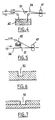
- FIGS. 1 to 3 show a passport 10 whose cover 20 is provided with a radiofrequency identification device 30, comprising a chip 31 and an antenna 32.
- a radiofrequency identification device 30 comprising a chip 31 and an antenna 32.
- the chip incorporates an antenna. This simplifies the incorporation of the radiofrequency identification device into the passport cover but has the disadvantage of reducing the range of the radio link that can be established with a reading device and / or writing.
- the chip 31 is preferably, as can be seen in Figures 1 and 2, near the fold 21 of the cover 20, for example in an area corresponding to a quarter of the width of the front flap 22 or rear 24 of the cover, measured from fold 21.
- the passport 10 comprises a notebook consisting of a set of sheets 11 having a guard page 12 stuck on the back of the front flap 22 of the cover.
- This page 12 is intended to receive an impression of variable mentions then to be covered by a film or "foil" transparent adhesive 13, applied by hot transfer.
- the cover 20 comprises a support layer 24, one face is covered by a layer 25 of a material capable of graining, and the outer surface of the cover 20 has a grain.
- the other face of the support layer 24 carries the chip 31 and its antenna 32 and is covered by a second layer 26, in the thickness of which is housed the chip 31.
- the face 27 of the layer 26, opposite to the layer 24 constitutes the inner surface of the cover 20.
- the antenna 32 When the antenna 32 is made by selective printing of a conductive ink on the layer 24, and has several turns, it may be necessary to locally deposit an insulator 34 on a portion of the turns to be able to carry on this insulation a bridge of electrical connection 35, always by selective deposition of a conductive ink, for connecting one end of the turns to the chip 31.
- the insulator 34 can be deposited, for example, by selective printing.
- the chip 31 can be connected to the antenna 32 according to well known methods, in particular by means of a conductive adhesive, or by thermo-compression or welding.
- the thickness of the layer 26 is greater than the thickness of the chip 31, so that the latter is protected from shocks by both the layer 26 and the layer 24.
- the thickness of the layer 26 is sufficiently large, so that in case of compression of the cover during the embellishment and passport-making processes, the layer 26 retains a thickness greater than that of the chip 31.
- the blanket is capable of undergoing the conventional graining and heat transfer treatments of the film 13 on the cover page 12.
- the cover 20 can be made in many ways, and the layers 24 and 26 can have different constitutions, and include a fibrous base.
- the multilayer structure illustrated in FIG. 3 is in no way limiting of the invention.
- a first sheet with a paper base (fibers of cellulose with or without synthetic fibers), which is saturated with styrene-butadiene copolymer latex to provide tear resistance and subsequent protection of the radiofrequency identification device.
- the chip and the antenna of the radiofrequency identification device are then deposited on one side of this first sheet, after drying, by a conventional method.
- the antenna can be made by screen printing by means of a conductive ink, and then the electrical connections to the chip can be made by thermo-compression.
- an insulator is deposited on part of the turns and an electrical connection bridge is made on this insulator between one end of the turns and the chip.
- the thickness of the first sheet may be of the order of 200 ⁇ m elsewhere, for example.
- FIG. 4 schematically shows the first sheet thus formed, with the chip 31 fixed on it.
- a paper of the blotter type of a thickness greater than that of the chip, is impregnated with a mixture based on polymer (s), for example styrene-butadiene, by passing it through an impregnation bath. to form a second sheet.
- the thickness of this second sheet may be of the order of 300 microns, for example.
- the two sheets are bonded thanks to the mixture of polymer (s) which has been impregnated with blotting paper and the latter matches the relief of the chip because of its compressibility to the wet state.
- the impregnating material is removed and the chip sinks into the blotter-type paper.
- the complex thus formed is then coated on one side, for example the outer face of the first sheet, with a mixture of polymers in order to impart a graining ability.
- the thickness of the layer deposited by coating is for example 50 microns.
- a printing varnish (matt or glossy) can be applied to the layer thus deposited, to improve the surface appearance and the resistance to the circulation.
- a paper of the blotter type of a thickness greater than that of the chip, for example of 300 ⁇ m in thickness, is brought into contact with a gluing machine 42 to impregnate one of its faces with a polymer such as a polyvinyl acetate, then this face thus coated is brought into contact with the first sheet between two rollers 41, as shown in Figure 5.
- the blotting paper saturated with polymer (s) and the first sheet previously manufactured, carrying the radiofrequency identification device on its inner side, bind, blotter-type paper marrying the relief of the chip because of its compressibility in the wet state.
- the complex thus formed is then coated on one of its faces, intended to constitute the outer surface of the cover, with a mixture of polymers having a graining ability.
- the thickness deposited by coating, for example on the outer face of the first sheet, may be of the order of 50 microns.
- a printing varnish (matte or glossy) can be deposited to improve the surface appearance and the resistance to the circulation.
- a first identical sheet is made to that of the previous examples, carrying the radio frequency identification device.
- a second sheet 53 is manufactured with a paper base, shown schematically in FIG. 6, having a hollow watermark 50, in the shape of the chip 31.
- the depth of the watermark 50 is slightly greater than the thickness of the chip 31.
- the thickness of the paper is for example of the order of 300 microns.
- the sheet 53 is preferably saturated with polymer (s) to ensure the subsequent protection of the chip.
- the sheet 53 After marking the locations of the chip 31 and the watermark 50, the sheet 53 is tackled with the first sheet previously made, so that the chip 31 is housed in the watermark 50.
- the bonding can be done cold. or hot. As the sheet 53 is still wet, the complex thus formed is passed between two rolls and proceed to drying.
- the face of the complex intended to constitute the outer surface of the passport may be coated with a mixture of polymers having a graining ability and deposit on this coating a printing varnish (glossy or matte) in order to improve the appearance of the surface and resistance to circulation.
- a printing varnish glossy or matte
- a first identical sheet is made to that of the previous examples, carrying the radio frequency identification device.
- a second sheet is manufactured with a hole made by laser etching or mechanically punch, this hole having a shape corresponding to that of the chip and a thickness at least greater than that of the chip.
- This second sheet may optionally be saturated with polymer (s) to ensure subsequent protection of the chip.
- the second sheet has for example a thickness of the order of 200 microns.
- a third sheet is also produced from a paper base which is preferably saturated with one or more synthetic or natural resins, for example elastomer latexes, by impregnation or precipitation in bulk, the impregnating material. being chosen so as to protect the radiofrequency identification device later.
- This third sheet has for example a thickness of the order of 100 microns.
- the three sheets are laminated spotted, the second sheet being applied to the first sheet having the chip, the latter being housed in the hole.
- the third sheet covers the second sheet on the opposite side to the first.
- the outer face of the first sheet is then coated with a polymer blend having a graining ability.
- a printing varnish gloss or matte
- gloss can be deposited on this coating to improve the surface appearance and the resistance to the circulation.
- a first identical sheet is made to that of the previous examples, carrying the radio frequency identification device.
- This sheet is then coated with a squeegee, on the face comprising the chip, with a "plastisol" type mixture based on PVC added with plasticizer and blowing agent.
- the whole is gelled in a tunnel oven at a temperature of the order of 200 ° C.
- the amounts of plasticizer and blowing agent are adjusted so that the coating has after gelation and cooling compressibility such that the thickness of the layer, during a depression or after a depression, remains greater than thickness of the chip, to protect the latter. For example, a thickness of the order of 300 ⁇ m is deposited.
- the layer deposited by coating can be grained after drying. This layer, after gelation and cooling, provides the desired mechanical characteristics.
- a glossy or matte printing varnish can be deposited on the coating to improve surface appearance and resistance to traffic.
- a sheet identical to the first sheet of the preceding examples is made, bearing the radiofrequency identification device.
- This sheet is then coated on the face carrying the radiofrequency identification device with a mixture based on a so-called "hotmelt” resin , comprising a hot-melt powder, for example polyurethane, using a suitable extrusion system. .
- a hotmelt resin comprising a hot-melt powder, for example polyurethane
- the polymer selected for the coating is chosen so as to have a compressibility such that the thickness of the layer deposited by coating, during a depression or after being seated in the event of impact, remains greater than the thickness of the chip, to protect the latter.
- the deposited thickness is for example of the order of 300 microns.
- the coating produced can be hot-marked to create the desired grain.
- a printing varnish gloss or matte
- a printing varnish can be deposited on the layer deposited by coating, possibly grained, to improve its surface appearance and the resistance to the circulation.
- a first sheet is produced from a paper base (cellulose fibers with or without synthetic fibers), optionally saturated with latex, and a first face of this paper base is coated with a mixture based on polymers exhibiting a graining ability, then possibly a printing varnish (glossy or matte) is deposited on this coating.
- the thickness of the paper base is for example of the order of 200 microns and the thickness of the layer capable of graining of the order of 50 microns.
- a cavity is then produced, at least of greater depth than that of the chip and having a shape adapted to that of the chip, by mechanical embossing on the second face of this paper base.
- the first face is grained simultaneously.
- a second sheet is made, moreover, from a paper base which is preferably saturated by mass impregnation or precipitation with synthetic or natural resins, for example elastomeric latexes, aimed at reinforcing its cohesion and subsequently protecting the device. radio frequency identification.
- the thickness of this second sheet is for example 200 microns.
- This second sheet which carries the chip and the antenna, is then counteracted on the first sheet, so that the chip is housed in the embossed cavity.
- a first sheet is made as in Example 7.
- a cavity of depth substantially equal to half that of the chip on this sheet is then made by mechanical embossing.
- a second sheet is made as in Example 3, with a watermark whose thickness is substantially equal to half that of the chip provided with its antenna, for example the IC-Link ® type of the company INSIDE TECHNOLOGIES.
- the two sheets are then assembled, the chip being completely housed in the cavities facing each of the sheets.
- a first sheet identical to that of the preceding example is produced.
- a conductive ink for example by screen printing, selectively to form two connection areas for the chip and an electrical connection bridge which will subsequently connect a end of the antenna to one of said connection areas.
- An insulating ink is then deposited, for example by screen printing, selectively to form a reserve at the connection areas and at the end of the connecting bridge opposite to the corresponding connection area.
- the turns of the antenna are made by depositing conductive ink, for example by screen printing.
- the ink used may contain tampering agents.
- the antenna is electrically connected at one of its ends to one of the above-mentioned connection areas and at the other end to the free end of the electrical connection bridge.
- Is deposited an insulating layer for example by screen printing, selectively, so as to form a reserve of a thickness at least equivalent to that of the chip and can accommodate it within the final structure without creating extra thickness.
- the thickness of the insulating layer deposited is for example of the order of 300 microns.
- the insulation may be deposited in one or more passes and may include an expansion agent.
- an insulating ink 34 is selectively deposited, and the electrical connection bridge 35 is made between one end of the turns and a connection zone for the chip.
- an insulating layer for example by screen printing, selectively, so as to form a thickness reserve at least equivalent to that of the chip.
- the chip Once the chip is placed in the cavity formed in the insulating layer, it can be covered with an optional protective layer.
- Example 2 The procedure is as in Example 1, with the difference that the chip and the antenna are carried by a thin flexible support such as a synthetic film, a polyester film for example.
- a thin flexible support such as a synthetic film, a polyester film for example.
- the support film, carrying the chip and the antenna, is then associated with a blotter-type sheet.
- the first sheet can be made, alternatively, from the outset with a coating capable of graining and / or receive a printing varnish.
- the material saturating the paper base of the first sheet of Examples 1 to 10 or the second sheet of Examples 1 to 4 may be a natural synthetic resin, for example an elastomer or a mixture of resins. material being selected to provide flexibility, improve tear strength, strain resistance upon compression and resilience. It is especially possible to use as copolymers of elastomer type, copolymers of styrene butadiene (SBR), polybutadiene (BR), butadiene-acrylonitrile copolymers (NBR), acrylic polymers, polychloroprene, polyisoprenes, this list not being limiting.
- SBR styrene butadiene
- BR polybutadiene
- NBR butadiene-acrylonitrile copolymers
- acrylic polymers polychloroprene, polyisoprenes
- polymer (s) used to confer the ability to graining there may be mentioned certain nitro-cellulosic polymers, polyurethanes, acrylic or vinyl.
- thermoplastic polymers based on PVC, polyurethanes and natural or synthetic elastomers.
- plasticized PVC or "plastisol” may be used, which contains plasticizers, for example esters of pthalic acid, odipic acid, sebacic acid or phosphoric acid.
- Polyurethane elastomers can also be used.
- a PVC emulsion can be further blended with other dispersions of butadiene / acrylonitrile copolymers or budatiene / acrylonitrile / styrene copolymer, which act as plasticizers.
- blowing agents functioning for example by an exothermic process.
- blowing agents include products such as azodicarbonanide or azo-sulfohydrazide-based Genitron® which, after decomposition at temperature, give gases such as nitrogen monoxide or hydrogen, carbon dioxide. or ammonia, resulting in the creation of cells and the swelling of the coating.
- water expansion agent in the case of a polyurethane type insulation made from thylene diisocyanate, polyester, and polyether.
- the paper base can be replaced by any other fibrous base, in particular a non-woven fabric.
- the cover may undergo embellishment treatments, in particular the application by heat transfer and under pressure of a colored or holographic metallized film, this film may be deposited on the cover before bonding the notebook or on the booklet after installation of the notebook.
- the cover can receive gravure printing or silk screen printing of a visible or invisible pattern, security or not.
- the cover may comprise a greater or lesser number of different layers.
- the antenna may be made other than by screen printing, for example by transfer of a film covered with copper conductive tracks made by etching.
- the invention is not limited to passports and also applies to the manufacture of family booklets or savings among others.
Landscapes
- Engineering & Computer Science (AREA)
- Computer Hardware Design (AREA)
- Microelectronics & Electronic Packaging (AREA)
- Physics & Mathematics (AREA)
- General Physics & Mathematics (AREA)
- Theoretical Computer Science (AREA)
- Textile Engineering (AREA)
- Credit Cards Or The Like (AREA)
- Laminated Bodies (AREA)
- Burglar Alarm Systems (AREA)
- Shielding Devices Or Components To Electric Or Magnetic Fields (AREA)
Claims (30)
- Mehrschichtstruktur, die einen Umschlag für ein Heft, insbesondere einen Reisepass, bildet, wobei die Mehrschichtstruktur dazu bestimmt ist, gemäß einem Falz des Umschlags gefaltet zu werden, umfassend eine einen Chip (31) aufweisende Funkfrequenzidentifizierungsvorrichtung (31, 32), wobei die die einzelnen Schichten der Mehrschichtstruktur bildenden Werkstoffe sowie die Dicke dieser Schichten so gewählt sind, dass der Umschlag (20) gegenüber mechanischen und thermischen Stößen beständig ist und einer Behandlung der Körnung und/oder Verzierung durch Auftrag einer Folie durch Wärmeübertragung und unter Druck und/oder der Laminierung bei Aufträgen von Sicherheitsfolien unterzogen werden kann, wobei die Struktur mindestens eine eine Faserbasis aufweisende Schicht umfasst, dadurch gekennzeichnet, dass der Chip ohne Erzeugung einer Verdickung in der Dicke einer ersten Schicht (26) untergebracht ist, deren Dicke größer als die des Chips (31) ist, so dass dieser gleichzeitig durch die erste Schicht (26) und durch eine Tragschicht (24) gegen Stöße geschützt ist, von der eine Seite mit der ersten Schicht (26) bedeckt ist, wobei die Dicke der ersten Schicht (26) so groß ist, dass während einer Komprimierung dieser Behandlung eine Dicke beibehalten wird, die größer als die des Chips (31) ist.
- Mehrschichtstruktur nach dem vorhergehenden Anspruch, dadurch gekennzeichnet, dass der Chip (31) in Nähe des Falzes (21) gelegen ist.
- Mehrschichtstruktur nach einem der Ansprüche 1 und 2, dadurch gekennzeichnet, dass die Faserbasis ein Zelluloselöschblatt oder ein Vlies ist.
- Mehrschichtstruktur nach dem vorhergehenden Anspruch, dadurch gekennzeichnet, dass die Faserbasis ein Polymermaterial enthält, das so gewählt ist, dass es der Mehrschichtstruktur einerseits Reißfestigkeitseigenschaften und andererseits Schlagzähigkeitseigenschaften verleiht, die ausreichen, um die Funkfrequenzidentifizierungsvorrichtung vor mechanischen Stößen zu schützen.
- Mehrschichtstruktur nach dem vorhergehenden Anspruch, dadurch gekennzeichnet, dass das Polymermaterial aus der folgenden Liste ausgewählt ist: natürliche oder synthetische Kautschuks, Styrol-Butadien-Kautschuk, Polybutadien, Butadien-Acrylonitril-Copolymere, Acrylpolymere, Polychloropren und ihre Mischungen.
- Mehrschichtstruktur nach einem der vorhergehenden Ansprüche, dadurch gekennzeichnet, dass die erste Schicht (26) eine Schlagzähigkeit aufweist, die ihr gestattet, im Fall einer momentanen Komprimierung eine Dicke beizubehalten, die größer oder gleich der Dicke des Chips ist.
- Mehrschichtstruktur nach Anspruch 6, dadurch gekennzeichnet, dass die erste Schicht (26) eine Faserbasis umfasst.
- Mehrschichtstruktur nach Anspruch 6 oder 7, dadurch gekennzeichnet, dass die erste Schicht (26) ein Polymermaterial umfasst, das so gewählt ist, dass es der Mehrschichtstruktur Schlagzähigkeitseigenschaften verleiht, die ausreichen, um die Funkfrequenzidentifizierungsvorrichtung vor mechanischen Stößen zu schützen.
- Mehrschichtstruktur nach einem der vorhergehenden Ansprüche, dadurch gekennzeichnet, dass sie eine Schicht aus einem für die Körnung geeigneten Material auf Polymerbasis umfasst, das insbesondere aus der folgenden Liste ausgewählt ist: Polymere auf der Basis von PVC, gegebenenfalls plastifiziert, von Polyurethanen oder natürlichen oder synthetischen Elastomeren, gegebenenfalls mit Treibmitteln, Emulsionen aus PVC und Butadien-Acrylonitril-Copolymer oder Butadien-Acrylonitril-Styrol-Copolymer und ihre Mischungen.
- Mehrschichtstruktur nach einem der vorhergehenden Ansprüche, dadurch gekennzeichnet, dass die Funkfrequenzidentifizierungsvorrichtung eine im Siebdruck hergestellte Antenne umfasst.
- Heftumschlag, umfassend eine Mehrschichtstruktur, wie sie in einem der Ansprüche 1 bis 10 definiert ist.
- Umschlag nach dem vorhergehenden Anspruch, dadurch gekennzeichnet, dass eine Seite der Tragschicht (24) mit einer zweiten Schicht (25) aus einem zur Körnung geeigneten Werkstoff bedeckt ist, wobei die Außenfläche des Umschlags (20) ein Korn aufweist.
- Umschlag nach einem der Ansprüche 11 und 12, umfassend eine metallisierte gefärbte oder holographische Folie, die durch einen Verzierungsarbeitsgang, insbesondere durch Wärmeübertragung und unter Druck, aufgebracht ist.
- Umschlag nach einem der Ansprüche 11 bis 13, umfassend einen Aufdruck eines sichtbaren oder unsichtbaren Musters durch Heliogravüre oder Siebdruck.
- Heft, umfassend einen Umschlag, wie er in einem der Ansprüche 11 bis 14 definiert ist, und eine Einheit von Blättern (11) mit einem Deckblatt (12), das auf die Rückseite der vorderen Klappe des Umschlags geklebt ist.
- Heft nach dem vorhergehenden Anspruch, wobei das Deckblatt (12) dazu bestimmt ist, einen Aufdruck von variablen Einträgen aufzunehmen und mit einer transparenten Klebefolie bedeckt zu werden.
- Heft nach einem der Ansprüche 15 und 16, wobei es ein Reisepass ist.
- Verfahren zur Herstellung einer Mehrschichtstruktur, wie sie in einem der Ansprüche 1 bis 10 definiert ist, umfassend den folgenden Schritt:- die Funkfrequenzidentifizierungsvorrichtung auf einer ersten Folie anordnen, und einen der folgenden Schritte:a) - diese erste Folie mit einer zweiten Folie so zusammenfügen, dass man eine resultierende, im Wesentlichen konstante Dicke erhält, wobei die zweite Folie zum Zeitpunkt der Zusammenfügung ausreichend komprimierbar ist, um den Chip in seiner Dicke aufzunehmen, oderb) - diese erste Folie mit einer zweiten Folie kaschieren, wobei der Chip der Funkfrequenzidentifizierungsvorrichtung auf der Innenseite der ersten Folie gelegen ist, wobei auf der zweiten Folie ein Loch oder ein Hohlraum gebildet ist, wobei dieses Loch oder dieser Hohlraum eine Form besitzt, die dafür ausgelegt ist, den Chip aufzunehmen, wobei der Chip bei der Kaschierung dieser Folien in das Loch oder den Hohlraum eingesetzt wird, oderc) - eine zweite Folie mit einem Loch bilden, das eine Form besitzt, die dafür ausgelegt ist, den Chip zu enthalten,- eine dritte Folie herstellen,- die drei Folien durch Kaschieren so zusammenfügen, dass die zweite Folie sandwichartig zwischen der ersten Folie und der dritten Folie angeordnet ist und dass der Chip in dem Loch der zweiten Folie untergebracht ist, oderd) - wenn vor dem Einsetzen der Funkfrequenzidentifizierungsvorrichtung eine Beschichtung mit einer Aussparung in Form eines Hohlraums hergestellt wurde, der eine Form besitzt, die dafür ausgelegt ist, den Chip auf der ersten Folie zu enthalten und die Funkfrequenzidentifizierungsvorrichtung in diesem Hohlraum auf der ersten Folie zu enthalten,- eine Beschichtung auf der Folie auf der Seite der Funkfrequenzidentifizierungsvorrichtung herstellen, so dass diese geschützt wird, oderwobei in den Schritten a) bis e) die Dicke der zweiten Folie oder der Beschichtung größer als diejenige des Chips ist und ausreichend groß ist, um während einer Komprimierung einer Behandlung der Körnung und/oder der Verzierung durch Auftrag einer Folie durch Wärmeübertragung und unter Druck und/oder der Laminierung bei Aufträgen von Sicherheitsfolien eine Dicke zu behalten, die größer als die des Chips ist.e) - auf der ersten Folie eine Beschichtung auftragen, die größer als die Dicke des Chips ist,
- Verfahren nach dem vorhergehenden Anspruch, dadurch gekennzeichnet, dass man b) ausführt und dass die erste Folie ebenfalls einen Hohlraum umfasst, in dem der Chip teilweise untergebracht wird.
- Verfahren nach einem der beiden vorhergehenden Ansprüche, dadurch gekennzeichnet, dass man die zweite Folie mit einem vertieften Wasserzeichen (50) herstellt, dessen Tiefe größer als die Dicke des Chips (31) ist, dass man den Chip auf der ersten Folie anordnet und dass man die zweite Folie mit der ersten Folie so kaschiert, dass der Chip (31) in dem Wasserzeichen (50) aufgenommen ist.
- Verfahren nach Anspruch 18, dadurch gekennzeichnet, dass man e) durchführt, wobei die Funkfrequenzidentifizierungsvorrichtung auf einer Seite der Folie aufgelegt wird, und dass diese Seite der Folie mit einer Mischung auf Basis eines nicht gelierten flüssigen Harzes beschichtet wird, wobei die aufgetragene Dicke größer als die des Chips ist.
- Verfahren nach dem vorhergehenden Anspruch, dadurch gekennzeichnet, dass die durch Beschichtung aufgetragene Schicht nach Trocknung gekörnt wird.
- Verfahren nach Anspruch 18, dadurch gekennzeichnet, dass man e) durchführt und dass man auf der die Funkfrequenzidentifizierungsvorrichtung tragenden Seite der Folie ein Harz auf Basis einer warmschmelzenden Verbindung aufträgt, wobei die aufgetragene Dicke größer als die Dicke des Chips ist.
- Verfahren nach dem vorhergehenden Anspruch, dadurch gekennzeichnet, dass man die Beschichtung warm prägt, um ein Korn zu erzeugen.
- Verfahren nach einem der Ansprüche 18 bis 24, dadurch gekennzeichnet, dass die erste Folie eine Faserbasis, insbesondere eine Papierbasis, umfasst, dass man diese Faserbasis mit einem Werkstoff, insbesondere einem Elastomerlatex, sättigt, der es gestattet, die Reißfestigkeit und den späteren Schutz der Funkfrequenzidentifizierungsvorrichtung zu gewährleisten, und dass man auf einer Seite dieser ersten Folie nach Trocknung den Chip und die Antenne der Funkfrequenzidentifizierungsvorrichtung auflegt.
- Verfahren nach einem der Ansprüche 18 bis 25, dadurch gekennzeichnet, dass die erste Folie mit einer für die Körnung geeigneten Mischung auf Polymerbasis beschichtet wird.
- Verfahren nach Anspruch 18, dadurch gekennzeichnet, dass man durch Beschichtung eine Mischung auf Polymerbasis aufträgt, die für die Körnung geeignet ist, und zwar nach Zusammenfügung der ersten und der zweiten Folie.
- Verfahren nach einem der Ansprüche 18 und 27, dadurch gekennzeichnet, dass man die zweite Folie mit einem thermoplastischen Polymer tränkt.
- Verfahren nach Anspruch 18, dadurch gekennzeichnet, dass man b) ausführt, wobei die erste Folie ausgehend von einer vorzugsweise mit Polymer, insbesondere einem Latex, gesättigten Faserbasis hergestellt ist, wobei diese erste Folie so geprägt ist, dass ein Hohlraum geschaffen wird, der eine an die Form des Chips angepasste Form besitzt, wobei eine zweite Folie ausgehend von einer Faserbasis hergestellt wird, die vorzugsweise durch Tränken oder Ausfällen in der Masse mit synthetischen oder natürlichen Harzen gesättigt ist, wobei auf dieser zweiten Folie ein Chip und eine Antenne aufgebracht sind, wobei diese zweite Folie mit der ersten Folie kaschiert wird, so dass der Chip in dem durch die Prägung geschaffenen Hohlraum untergebracht wird.
- Verfahren nach einem der Ansprüche 18 bis 24, dadurch gekennzeichnet, dass der Chip und die Antenne auf einer Tragfolie, insbesondere einer Polyesterfolie, befestigt werden, bevor sie mit einer Faserbasis kombiniert werden.
Priority Applications (1)
| Application Number | Priority Date | Filing Date | Title |
|---|---|---|---|
| EP06022214.8A EP1768051B1 (de) | 2001-04-26 | 2002-04-25 | Umschlag für einen Reisepass, der eine Vorrichtung zur Radiofrequenzidentifikation einschließt |
Applications Claiming Priority (3)
| Application Number | Priority Date | Filing Date | Title |
|---|---|---|---|
| FR0105616A FR2824018B1 (fr) | 2001-04-26 | 2001-04-26 | Couverture incorporant un dispositif d'identification radiofrequence |
| FR0105616 | 2001-04-26 | ||
| PCT/FR2002/001423 WO2002089052A1 (fr) | 2001-04-26 | 2002-04-25 | Couverture incorporant un dispositif d'identification radiofrequence |
Related Child Applications (1)
| Application Number | Title | Priority Date | Filing Date |
|---|---|---|---|
| EP06022214.8A Division EP1768051B1 (de) | 2001-04-26 | 2002-04-25 | Umschlag für einen Reisepass, der eine Vorrichtung zur Radiofrequenzidentifikation einschließt |
Publications (3)
| Publication Number | Publication Date |
|---|---|
| EP1382011A1 EP1382011A1 (de) | 2004-01-21 |
| EP1382011B1 true EP1382011B1 (de) | 2007-02-21 |
| EP1382011B8 EP1382011B8 (de) | 2007-04-18 |
Family
ID=8862717
Family Applications (2)
| Application Number | Title | Priority Date | Filing Date |
|---|---|---|---|
| EP06022214.8A Expired - Lifetime EP1768051B1 (de) | 2001-04-26 | 2002-04-25 | Umschlag für einen Reisepass, der eine Vorrichtung zur Radiofrequenzidentifikation einschließt |
| EP02727693A Revoked EP1382011B8 (de) | 2001-04-26 | 2002-04-25 | Abdeckung mit radiofrequenzidentifikationsgerät |
Family Applications Before (1)
| Application Number | Title | Priority Date | Filing Date |
|---|---|---|---|
| EP06022214.8A Expired - Lifetime EP1768051B1 (de) | 2001-04-26 | 2002-04-25 | Umschlag für einen Reisepass, der eine Vorrichtung zur Radiofrequenzidentifikation einschließt |
Country Status (16)
| Country | Link |
|---|---|
| US (2) | US7847698B2 (de) |
| EP (2) | EP1768051B1 (de) |
| AR (1) | AR035870A1 (de) |
| AT (1) | ATE354835T1 (de) |
| AU (1) | AU2002257891B2 (de) |
| BR (1) | BR0205103A (de) |
| CA (1) | CA2414244C (de) |
| CY (1) | CY1106466T1 (de) |
| DE (1) | DE60218295T2 (de) |
| DK (1) | DK1382011T3 (de) |
| ES (2) | ES2280535T3 (de) |
| FR (1) | FR2824018B1 (de) |
| PE (1) | PE20021124A1 (de) |
| PT (1) | PT1382011E (de) |
| UA (1) | UA76715C2 (de) |
| WO (1) | WO2002089052A1 (de) |
Cited By (2)
| Publication number | Priority date | Publication date | Assignee | Title |
|---|---|---|---|---|
| EP2116390A2 (de) | 2008-05-09 | 2009-11-11 | Austria Card Plastikkarten und Ausweissysteme Gesellschaft MBH | Reisepass mit laserfähiger Personalisierseite und Vlieseinlage |
| US7872579B2 (en) | 2004-04-14 | 2011-01-18 | Arjowiggins Security | Structure including an electronic device, in particular for fabricating a security document or a document of value |
Families Citing this family (87)
| Publication number | Priority date | Publication date | Assignee | Title |
|---|---|---|---|---|
| US6783067B2 (en) * | 2000-01-28 | 2004-08-31 | Datacard Corporation | Passport production system and method |
| JP2003216908A (ja) * | 2002-01-22 | 2003-07-31 | Hitachi Electronics Service Co Ltd | パスポート偽造検出装置 |
| US20030151028A1 (en) * | 2002-02-14 | 2003-08-14 | Lawrence Daniel P. | Conductive flexographic and gravure ink |
| WO2004080726A2 (de) * | 2003-03-12 | 2004-09-23 | Bundesdruckerei Gmbh | Verfahren zur herstellung einer buchdeckeneinlage und eines buchartigen wertdokumentes sowie eine buchdeckeneinlage und ein buchartiges wertdokument |
| DE10338444B4 (de) * | 2003-08-18 | 2019-11-28 | Smartrac Ip B.V. | Transponderinlay für ein Dokument zur Personenidentifikation sowie Verfahren zu dessen Herstellung |
| ATE391965T1 (de) * | 2003-09-16 | 2008-04-15 | Kugler Womako Gmbh | Verfahren und vorrichtung zum einbringen einer elektronischen schaltkreisanordnung in ein buchförmiges dokument sowie hiernach hergestelltes buchförmiges dokument |
| DE10342946A1 (de) † | 2003-09-17 | 2005-04-28 | Bundesdruckerei Gmbh | Einlageblatt für ein buchartiges Identifikationsdokument, buchartiges Identifikationsdokument und Verfahren zur Herstellung eines buchartigen Identifikationsdokuments |
| WO2005034031A1 (en) * | 2003-10-01 | 2005-04-14 | Axalto Sa | Identification document |
| EP1521208A1 (de) * | 2003-10-01 | 2005-04-06 | Axalto S.A. | Elektronisches Identifikationsdokument |
| JP4066929B2 (ja) * | 2003-10-08 | 2008-03-26 | 株式会社日立製作所 | 電子装置及びその製造方法 |
| FR2863083B1 (fr) * | 2003-12-02 | 2006-03-03 | A S K | Livret d'identite a dispositif d'indentification radiofrequence |
| US7259678B2 (en) * | 2003-12-08 | 2007-08-21 | 3M Innovative Properties Company | Durable radio frequency identification label and methods of manufacturing the same |
| FR2863748B1 (fr) * | 2003-12-12 | 2006-02-24 | Thales Sa | Document securise a puce sans contact avec masquage des donnees |
| WO2005062246A1 (en) * | 2003-12-19 | 2005-07-07 | Axalto Sa | Identification document |
| DE102004007731A1 (de) * | 2004-02-16 | 2005-09-01 | Multitape Gmbh | Passdokument und Verfahren zur Herstellung desselben |
| DE102004008840A1 (de) * | 2004-02-20 | 2005-09-01 | Bundesdruckerei Gmbh | Verfahren zur Herstellung eines buchartigen Wertdokuments sowie ein buchartiges Wertdokument |
| US7421245B2 (en) * | 2004-02-20 | 2008-09-02 | 3M Innovative Properties Company | Field-shaping shielding for radio frequency identification (RFID) system |
| JP2005276176A (ja) * | 2004-02-27 | 2005-10-06 | Toshiba Corp | 携帯可能電子装置 |
| DE102004011489A1 (de) | 2004-03-09 | 2005-09-29 | Giesecke & Devrient Gmbh | Ausweisdokument mit einem integrierten Schaltkreis |
| FR2868575B1 (fr) * | 2004-04-06 | 2006-06-16 | Datacard Inc | Machine de personnalisation a haute cadence |
| JP5198059B2 (ja) * | 2004-04-14 | 2013-05-15 | スマート‐ガード、エルエルシー | 隠されたセキュリティー装置付きハードカバー製品 |
| US7183918B1 (en) * | 2004-04-14 | 2007-02-27 | Smartguard, Llc | Intermediate cover board with concealed security device for hard cover product |
| US8072330B1 (en) | 2004-04-14 | 2011-12-06 | Smartguard, Llc | Hard cover product with concealed printed security device |
| US7557717B2 (en) * | 2004-04-14 | 2009-07-07 | Smartguard, Llc | Hard cover product with concealed security device |
| US7411499B2 (en) * | 2004-04-14 | 2008-08-12 | Smartguard, Llc | Hard cover product with concealed security device |
| US7233246B2 (en) * | 2004-04-14 | 2007-06-19 | Smartguard, Llc | Hard cover product with spine-disposed concealed security device |
| FR2869706B1 (fr) * | 2004-04-29 | 2006-07-28 | Oberthur Card Syst Sa | Entite electronique securisee, telle qu'un passeport. |
| DE102004027125A1 (de) * | 2004-06-03 | 2005-12-22 | Joergen Brosow | Sicherheitsdokument |
| US20060005050A1 (en) * | 2004-06-10 | 2006-01-05 | Supercom Ltd. | Tamper-free and forgery-proof passport and methods for providing same |
| ITMO20040146A1 (it) * | 2004-06-11 | 2004-09-11 | Windinglab S R L | Dispositivo di identificazione a radio-frequenza |
| ES2373029T3 (es) | 2004-06-16 | 2012-01-30 | Gemalto Sa | Documento electrónico blindado sin contacto. |
| DE102004039567A1 (de) * | 2004-08-13 | 2006-02-23 | Ovd Kinegram Ag | Individualisiertes Sicherheitsdokument |
| US20060065744A1 (en) * | 2004-09-15 | 2006-03-30 | Fuji Xerox Co., Ltd. | IC-tag-attached sheet and image forming apparatus |
| US7591415B2 (en) * | 2004-09-28 | 2009-09-22 | 3M Innovative Properties Company | Passport reader for processing a passport having an RFID element |
| DE102004048361A1 (de) * | 2004-10-01 | 2006-04-13 | Bundesdruckerei Gmbh | Buchartiges Wertdokument |
| DE102005021477B4 (de) * | 2004-10-14 | 2020-04-02 | Pav Card Gmbh | Verfahren zum Herstellen eines Laminats für ein Pass-Inlay und Ausweisdokument |
| EP1819529A1 (de) * | 2004-11-17 | 2007-08-22 | Brite IP Limited | Geformter blatt-artikel |
| FR2879789B1 (fr) * | 2004-12-17 | 2008-07-18 | Francois Charles Oberthur Fidu | Document de securite pourvu de moyens de perturbation de champ electromagnetique |
| FR2881251B1 (fr) * | 2005-01-24 | 2007-04-13 | Ask Sa | Livret d'identite a dispositif d'identification radiofrequence resistant aux milieux humides |
| FR2881252A1 (fr) | 2005-01-24 | 2006-07-28 | Ask Sa | Dispositif d'idenfication radiofrequence resistant aux milieux et son procede de fabrication |
| US11295095B2 (en) | 2005-02-07 | 2022-04-05 | Mynette Technologies, Inc. | Secure reading of passport RFID tags |
| US11170185B2 (en) | 2005-02-07 | 2021-11-09 | Steven Michael Colby | State dependent passport reading |
| US11270182B2 (en) | 2005-02-07 | 2022-03-08 | Mynette Technologies, Inc. | RFID financial device including mechanical switch |
| FR2882174B1 (fr) | 2005-02-11 | 2007-09-07 | Smart Packaging Solutions Sps | Procede de fabrication d'un dispositif microelectronique a fonctionnement sans contact notamment pour passeport electronique |
| GB0503138D0 (en) | 2005-02-15 | 2005-03-23 | Rue De Int Ltd | Flexible sheet assembly |
| DE102005010364A1 (de) * | 2005-03-03 | 2006-09-07 | Bundesdruckerei Gmbh | Buchartiges Dokument, insbesondere Identifikationsdokument |
| US7479882B2 (en) * | 2005-04-14 | 2009-01-20 | Flexilis, Inc. | RFID security system and methods |
| US11347949B2 (en) | 2005-05-06 | 2022-05-31 | Mynette Technologies, Inc. | Cellular device including inductive antenna |
| GB0511842D0 (en) * | 2005-06-10 | 2005-07-20 | Rue De Int Ltd | Booklet cover |
| FR2888371B1 (fr) * | 2005-07-06 | 2007-10-05 | Oberthur Card Syst Sa | Support de donnees pliable a puce sans contact tel qu'un passeport |
| FR2888367B1 (fr) | 2005-07-07 | 2007-10-19 | Oberthur Card Syst Sa | Document a dispositif electronique sans contact integre a resonateur. |
| FR2888368B1 (fr) * | 2005-07-07 | 2007-10-05 | Oberthur Card Syst Sa | Document pliable a dispositif electronique sans contact a perturbateur |
| DE102005038092A1 (de) * | 2005-08-11 | 2007-02-15 | Giesecke & Devrient Gmbh | Verfahren und Einrichtung zur Prüfung eines elektronischen Passes |
| JP4754344B2 (ja) * | 2005-12-20 | 2011-08-24 | 富士通株式会社 | Rfidタグ |
| FR2899000B1 (fr) * | 2006-03-24 | 2008-10-17 | Arjowiggins Security Soc Par A | Dispositif radiofrequence comportant un composant electronique pourvu d'une antenne integree et couplee electromagnetiquement a une antenne d'amplification |
| JP2009535874A (ja) * | 2006-04-28 | 2009-10-01 | アエスカ エス.ア. | Rfidデバイスの支持体及びその製造方法 |
| FR2900484B3 (fr) * | 2006-04-28 | 2008-08-08 | Ask Sa | Support de dispositif d'identification radiofrequence et son procede de fabrication |
| FR2900485B3 (fr) * | 2006-04-28 | 2008-08-08 | Ask Sa | Support de dispositif d'identification radiofrequence et son procede de fabrication |
| EP2084654B1 (de) | 2006-05-17 | 2012-10-17 | Landqart | Flexibler schichtaufbau mit integriertem schaltkreis |
| FR2892843B1 (fr) * | 2006-11-14 | 2008-12-12 | Arjowiggins Security Soc Par A | Structure comportant un dispositif electronique, notamment pour la fabrication d'un document de securite ou de valeur. |
| FR2918485B1 (fr) * | 2007-07-04 | 2010-09-10 | Arjowiggins Licensing Sas | Support fibreux pour insert comportant une antenne |
| FR2922342B1 (fr) * | 2007-10-11 | 2010-07-30 | Ask Sa | Support de dispositif d'identification radiofrequence renforce et son procede de fabrication |
| FR2932711B1 (fr) * | 2008-06-23 | 2012-01-20 | Michelin Soc Tech | Procede et installation de fabrication d'un composant electronique enrobe de gomme. |
| DE102008034984C5 (de) * | 2008-07-25 | 2018-06-14 | Atlantic Zeiser Gmbh | Verfahren zur Herstellung einer Kunststoffkarte |
| FR2935060B1 (fr) * | 2008-08-12 | 2010-09-10 | Arjowiggins Licensing Sas | E-document comportant un element de perturbation electromagnetique |
| FR2936075B1 (fr) * | 2008-09-12 | 2010-12-31 | Arjowiggins Licensing Sas | Structure comportant au moins deux dispositifs a microcircuit integre a communication sans contact |
| EP2177922A1 (de) | 2008-10-15 | 2010-04-21 | Gemalto SA | Prüfverfahren eines elektronischen Identitätsdokuments und entsprechende Vorrichtung |
| KR100933175B1 (ko) * | 2009-02-05 | 2009-12-21 | 이영범 | 보안문서 관제시스템 및 관제방법 |
| US20100307944A1 (en) * | 2009-05-04 | 2010-12-09 | Johnson Christopher A | System and method for distribution of personalized books |
| WO2010132117A1 (en) * | 2009-05-13 | 2010-11-18 | American Bank Note Company | Cover and method of manufacturing the same |
| EP2261054A1 (de) * | 2009-06-12 | 2010-12-15 | Gemalto Oy | Verfahren zur Herstellung einer Sicherheitsseite |
| CA2790702A1 (en) * | 2010-03-19 | 2011-09-22 | Jostens, Inc. | System and method for creating customized products |
| CN103026372A (zh) * | 2010-06-18 | 2013-04-03 | 微连接股份公司 | 多层柔性印刷电路和制造方法 |
| FR2963137B1 (fr) * | 2010-07-20 | 2016-02-19 | Oberthur Technologies | Insert a transpondeur et dispositif comprenant un tel insert |
| FR2965511B1 (fr) | 2010-10-05 | 2016-12-02 | Oberthur Technologies | Document de securite comprenant un dispositif de communication en champ proche tel qu'un passeport |
| KR101106974B1 (ko) * | 2011-06-03 | 2012-01-20 | 주식회사 테스나 | 여권표지 |
| EP2555139A1 (de) * | 2011-08-02 | 2013-02-06 | Gemalto SA | Gesichertes Dokument, das eine Vorrichtung zur Funkidentifikation einschließt |
| US8950681B2 (en) | 2011-11-07 | 2015-02-10 | Blackberry Limited | Universal integrated circuit card apparatus and related methods |
| USD691610S1 (en) | 2011-11-07 | 2013-10-15 | Blackberry Limited | Device smart card |
| US8763914B2 (en) * | 2012-01-17 | 2014-07-01 | On Track Innovations Ltd. | Decoupled contactless bi-directional systems and methods |
| CN102689544B (zh) * | 2012-06-14 | 2016-08-17 | 黑龙江大学 | 多功能日记本 |
| US9785880B2 (en) * | 2015-11-06 | 2017-10-10 | Bank Of America Corporation | Radio frequency identification activation |
| NL2016003B1 (en) * | 2015-12-22 | 2017-07-03 | Trespa Int Bv | A decorative panel. |
| USD821401S1 (en) * | 2016-01-29 | 2018-06-26 | Siebels Asset Management Research, Ltd. | Controlled document tracking and/or authentication device |
| US10546227B2 (en) | 2017-05-11 | 2020-01-28 | Building Materials Investment Corporation | TPO and PVC membrane incorporating RFID tags |
| DE102018004914B4 (de) * | 2018-06-20 | 2024-06-06 | Mühlbauer Gmbh & Co. Kg | Fertigungsanlage für die Herstellung von Sicherheits- oder Buchdokumenten |
| BR112021017570A2 (pt) * | 2019-03-07 | 2021-11-09 | Covestro Intellectual Property Gmbh & Co Kg | Estrutura em camadas para produzir uma dobradiça, em particular, para produzir capas de livros de múltiplas camadas |
Family Cites Families (50)
| Publication number | Priority date | Publication date | Assignee | Title |
|---|---|---|---|---|
| US3922424A (en) | 1972-05-22 | 1975-11-25 | Monsanto Co | Non-woven fibrous material bonded with ethylene/vinyl chloride interpolymers |
| US3972764A (en) * | 1972-08-28 | 1976-08-03 | Bookwrights, Inc. | Plastic book cover and method of making |
| DE2919649A1 (de) | 1979-05-16 | 1980-11-20 | Bbc Brown Boveri & Cie | Sicherheitspapier |
| DE3019207A1 (de) * | 1980-05-20 | 1981-11-26 | GAO Gesellschaft für Automation und Organisation mbH, 8000 München | Traegerelement fuer einen ic-chip |
| FR2509767A1 (fr) | 1981-07-20 | 1983-01-21 | Arjomari Prioux | Nouveau papier synthetique leger imprimable et son procede de preparation |
| DE3143208C2 (de) * | 1981-10-30 | 1984-07-05 | Max-E. Dipl.-Ing. 7320 Göppingen Reeb | Identifizierungsanordnung in Form eines an einem Gegenstand anbringbaren etikettartigen Streifens und Verfahren zu deren Herstellung |
| US5265428A (en) | 1990-10-05 | 1993-11-30 | Exxon Production Research Company | Bubble cap tray for melting solids and method for using same |
| AU4026693A (en) | 1992-04-07 | 1993-11-08 | Intelicard Technologies, Inc. | Process and system for reading and writing images and related data to an integrated circuit card |
| FR2691563B1 (fr) * | 1992-05-19 | 1996-05-31 | Francois Droz | Carte comprenant au moins un element electronique et procede de fabrication d'une telle carte. |
| GB9211123D0 (en) | 1992-05-26 | 1992-07-08 | Amblehurst Ltd | Holographic device |
| GB9222460D0 (en) | 1992-10-26 | 1992-12-09 | Hughes Microelectronics Europa | Radio frequency baggage tag |
| CA2122168A1 (en) | 1993-12-16 | 1995-06-17 | David P. Hultman | Polymer-reinforced paper having improved cross-direction tear |
| US5751256A (en) * | 1994-03-04 | 1998-05-12 | Flexcon Company Inc. | Resonant tag labels and method of making same |
| DE4416697A1 (de) | 1994-05-11 | 1995-11-16 | Giesecke & Devrient Gmbh | Datenträger mit integriertem Schaltkreis |
| US5528222A (en) * | 1994-09-09 | 1996-06-18 | International Business Machines Corporation | Radio frequency circuit and memory in thin flexible package |
| DE19601358C2 (de) | 1995-01-20 | 2000-01-27 | Fraunhofer Ges Forschung | Papier mit integrierter Schaltung |
| DE19654902C2 (de) | 1996-03-15 | 2000-02-03 | David Finn | Chipkarte |
| US5847649A (en) * | 1996-03-25 | 1998-12-08 | Minnesota Mining And Manufacturing Company | EAS marker assemblies |
| US5786626A (en) * | 1996-03-25 | 1998-07-28 | Ibm Corporation | Thin radio frequency transponder with leadframe antenna structure |
| WO1998002848A1 (de) | 1996-07-11 | 1998-01-22 | David Finn | Verfahren und vorrichtung zur herstellung einer chipkarte sowie chipkarte |
| US5895557A (en) | 1996-10-03 | 1999-04-20 | Kimberly-Clark Worldwide, Inc. | Latex-saturated paper |
| US6111506A (en) * | 1996-10-15 | 2000-08-29 | Iris Corporation Berhad | Method of making an improved security identification document including contactless communication insert unit |
| FR2768443B1 (fr) | 1997-09-15 | 1999-10-15 | Arjo Wiggins Papiers Couches | Papier couche comportant une marque ressemblant a un filigrane et procede de fabrication |
| EP0905657B1 (de) | 1997-09-23 | 2003-05-28 | STMicroelectronics S.r.l. | Banknote mit einer integrierten Schaltung |
| FR2769109B1 (fr) | 1997-09-26 | 1999-11-19 | Gemplus Sca | Dispositif electronique a puce jetable et procede de fabrication |
| US5973599A (en) * | 1997-10-15 | 1999-10-26 | Escort Memory Systems | High temperature RFID tag |
| FR2775533B1 (fr) | 1998-02-27 | 2003-02-14 | Gemplus Sca | Dispositif electronique a memoire electronique sans contact, et procede de fabrication d'un tel dispositif |
| FR2776153B1 (fr) | 1998-03-10 | 2000-07-28 | Ordicam Rech Et Dev | Procede pour l'identification securitaire d'une personne et dispositif portatif pour la mise en oeuvre du procede |
| US6608911B2 (en) * | 2000-12-21 | 2003-08-19 | Digimarc Corporation | Digitally watermaking holograms for use with smart cards |
| NL1008929C2 (nl) * | 1998-04-20 | 1999-10-21 | Vhp Ugchelen Bv | Uit papier vervaardigd substraat voorzien van een geïntegreerde schakeling. |
| US6094137A (en) * | 1998-04-22 | 2000-07-25 | Rasch; Arnan R. | Book binding, machine, and method for incorporating electronic article surveillance marker into a book |
| US6064855A (en) * | 1998-04-27 | 2000-05-16 | Ho; Frederick Pak Wai | Voice book system |
| JP4311506B2 (ja) | 1998-06-04 | 2009-08-12 | コニカミノルタエムジー株式会社 | Ic冊子 |
| JPH11348470A (ja) | 1998-06-05 | 1999-12-21 | Konica Corp | Ic冊子 |
| JPH11348471A (ja) | 1998-06-05 | 1999-12-21 | Konica Corp | 冊子及びicカードホルダ |
| US5914657A (en) * | 1998-06-26 | 1999-06-22 | Chen; Vencent | Wallet capable of preventing loss of cards kept therein |
| US6100804A (en) * | 1998-10-29 | 2000-08-08 | Intecmec Ip Corp. | Radio frequency identification system |
| DE19850353C1 (de) | 1998-11-02 | 2000-03-16 | David Finn | Identifikationslabel sowie Verfahren zur Herstellung eines Indentifikationslabels |
| NL1010841C2 (nl) | 1998-12-18 | 2000-06-20 | Enschede Sdu Bv | Werkwijze voor het vervaardigen van een boekje, boekje vervaardigd volgens de werkwijze en boekje. |
| US6262692B1 (en) * | 1999-01-13 | 2001-07-17 | Brady Worldwide, Inc. | Laminate RFID label and method of manufacture |
| EP1049043A1 (de) * | 1999-04-30 | 2000-11-02 | Siemens Aktiengesellschaft | Chip-Träger-Verbund |
| US6395124B1 (en) | 1999-07-30 | 2002-05-28 | 3M Innovative Properties Company | Method of producing a laminated structure |
| JP4588139B2 (ja) | 1999-08-31 | 2010-11-24 | リンテック株式会社 | Icカードの製造方法 |
| JP2001092934A (ja) | 1999-09-20 | 2001-04-06 | Toshiba Corp | 無線情報記憶媒体、無線情報記憶媒体の製造方法、無線情報記憶媒体を備えた冊子体、無線情報記憶媒体を用いた身分確認システム、および無線情報記憶媒体の発行システム |
| DE19950145C1 (de) * | 1999-10-18 | 2001-05-10 | Lucatron Ag Baar | Verfahren zum Auslesen und Beschreiben von RFID-Transpondern |
| US7006116B1 (en) * | 1999-11-16 | 2006-02-28 | Nokia Corporation | Tangibly encoded media identification in a book cover |
| US6254953B1 (en) * | 1999-12-02 | 2001-07-03 | World Color Printing Division, Inc. | Antitheft hang tag folded and secured to conceal antitheft marker |
| US6281795B1 (en) * | 2000-02-08 | 2001-08-28 | Moore North America, Inc. | RFID or EAS label mount with double sided tape |
| JP2003211878A (ja) * | 2002-01-21 | 2003-07-30 | Hitachi Electronics Service Co Ltd | 偽造防止用idチップ付きパスポート |
| UA56835A (uk) | 2002-09-27 | 2003-05-15 | Харківський Державний Медичний Університет | Спосіб оцінки рівня якості здоров'я пацієнтів з хронічними захворюваннями шлунково-кишкового тракту |
-
2001
- 2001-04-26 FR FR0105616A patent/FR2824018B1/fr not_active Expired - Fee Related
-
2002
- 2002-04-25 ES ES02727693T patent/ES2280535T3/es not_active Expired - Lifetime
- 2002-04-25 ES ES06022214T patent/ES2433068T3/es not_active Expired - Lifetime
- 2002-04-25 DK DK02727693T patent/DK1382011T3/da active
- 2002-04-25 AU AU2002257891A patent/AU2002257891B2/en not_active Ceased
- 2002-04-25 DE DE60218295T patent/DE60218295T2/de not_active Expired - Lifetime
- 2002-04-25 CA CA002414244A patent/CA2414244C/fr not_active Expired - Fee Related
- 2002-04-25 WO PCT/FR2002/001423 patent/WO2002089052A1/fr not_active Ceased
- 2002-04-25 BR BR0205103-6A patent/BR0205103A/pt not_active IP Right Cessation
- 2002-04-25 AT AT02727693T patent/ATE354835T1/de active
- 2002-04-25 PT PT02727693T patent/PT1382011E/pt unknown
- 2002-04-25 EP EP06022214.8A patent/EP1768051B1/de not_active Expired - Lifetime
- 2002-04-25 US US10/312,009 patent/US7847698B2/en not_active Expired - Fee Related
- 2002-04-25 UA UA20021210476A patent/UA76715C2/uk unknown
- 2002-04-25 EP EP02727693A patent/EP1382011B8/de not_active Revoked
- 2002-04-26 AR ARP020101520A patent/AR035870A1/es active IP Right Grant
- 2002-04-26 PE PE2002000357A patent/PE20021124A1/es not_active Application Discontinuation
-
2007
- 2007-05-07 CY CY20071100600T patent/CY1106466T1/el unknown
-
2010
- 2010-07-15 US US12/805,166 patent/US7940185B2/en not_active Expired - Fee Related
Cited By (3)
| Publication number | Priority date | Publication date | Assignee | Title |
|---|---|---|---|---|
| US7872579B2 (en) | 2004-04-14 | 2011-01-18 | Arjowiggins Security | Structure including an electronic device, in particular for fabricating a security document or a document of value |
| EP2116390A2 (de) | 2008-05-09 | 2009-11-11 | Austria Card Plastikkarten und Ausweissysteme Gesellschaft MBH | Reisepass mit laserfähiger Personalisierseite und Vlieseinlage |
| DE102008023045A1 (de) | 2008-05-09 | 2009-11-12 | Austria Card Plastikkarten Und Ausweissysteme Gmbh | Reisepass mit laserfähiger Personalisierseite und Vlieseinlage |
Also Published As
| Publication number | Publication date |
|---|---|
| US7847698B2 (en) | 2010-12-07 |
| DE60218295T2 (de) | 2007-10-31 |
| US20030168514A1 (en) | 2003-09-11 |
| EP1382011A1 (de) | 2004-01-21 |
| ATE354835T1 (de) | 2007-03-15 |
| CA2414244C (fr) | 2008-11-25 |
| BR0205103A (pt) | 2003-05-20 |
| CY1106466T1 (el) | 2012-01-25 |
| UA76715C2 (uk) | 2006-09-15 |
| DE60218295D1 (de) | 2007-04-05 |
| EP1768051A3 (de) | 2010-01-20 |
| FR2824018A1 (fr) | 2002-10-31 |
| EP1382011B8 (de) | 2007-04-18 |
| EP1768051A2 (de) | 2007-03-28 |
| WO2002089052A1 (fr) | 2002-11-07 |
| PE20021124A1 (es) | 2003-02-07 |
| PT1382011E (pt) | 2007-05-31 |
| AR035870A1 (es) | 2004-07-21 |
| EP1768051B1 (de) | 2013-08-07 |
| AU2002257891B2 (en) | 2005-07-07 |
| ES2433068T3 (es) | 2013-12-09 |
| FR2824018B1 (fr) | 2003-07-04 |
| DK1382011T3 (da) | 2007-06-18 |
| US20100282855A1 (en) | 2010-11-11 |
| US7940185B2 (en) | 2011-05-10 |
| CA2414244A1 (fr) | 2002-11-07 |
| ES2280535T3 (es) | 2007-09-16 |
Similar Documents
| Publication | Publication Date | Title |
|---|---|---|
| EP1382011B1 (de) | Abdeckung mit radiofrequenzidentifikationsgerät | |
| EP1448392B1 (de) | Verfahren zur herstellung eines artikels aus einer folie und mindestens einem direkt daran befestigten element | |
| EP1745419B1 (de) | Struktur mit einer elektronischen einrichtung insbesondere zur herstellung eines sicherheit- oder wertdokuments | |
| FR2769541A1 (fr) | Procede d'impression de motifs multicolores sur un film flocke thermocollant ou soudable par haute frequence, film obtenu par ce procede, procede d'application de ce film sur un support a decorer et support decore obtenu par ce procede | |
| EP0606556A1 (de) | Dekorationsverfahren für die Oberseite des skis | |
| FR2769440A1 (fr) | Procede pour la fabrication d'un dispositif electronique a puce et/ou a antenne et dispositif obtenu par le procede | |
| EP2321771B1 (de) | E-dokument mit einem elektromagnetischen störungselement | |
| FR2877462A1 (fr) | Structure comportant un dispositif electronique pour la fabrication d'un document de securite. | |
| US20030077463A1 (en) | Resin molded product having metallic luster surface | |
| EP0984864B1 (de) | Vorläufige fiche, vorrichtung und verfahren zum herstellen von dokumenten mit wechselende aufschriften | |
| EP0774280B1 (de) | Verfahren zur Herstellung eines Halbfabrikats zum Dekorieren von Gleitbrettern | |
| FR2652539A1 (fr) | Lamine decoratif souple comportant un feuillet apparent de bois tranche ou deroule, et procede de fabrication. | |
| WO2021219630A1 (fr) | Procede de fabrication d'une carte a puce comportant du bois et conforme au standard des cartes a puce | |
| EP1924961B1 (de) | Aus einem aufkleber bestehendes identitäts- und sicherheitsdokument | |
| WO2009122020A1 (fr) | Feuille transfert pour support thermosensible | |
| FR2892843A1 (fr) | Structure comportant un dispositif electronique, notamment pour la fabrication d'un document de securite ou de valeur. | |
| FR2980139A1 (fr) | Document securise et methode de fabrication dudit document securise | |
| FR2763890A1 (fr) | Fiche intermediaire, procede et dispositif pour la preparation d'un document portant des inscriptions variables |
Legal Events
| Date | Code | Title | Description |
|---|---|---|---|
| PUAI | Public reference made under article 153(3) epc to a published international application that has entered the european phase |
Free format text: ORIGINAL CODE: 0009012 |
|
| 17P | Request for examination filed |
Effective date: 20021210 |
|
| AK | Designated contracting states |
Kind code of ref document: A1 Designated state(s): AT BE CH CY DE DK ES FI FR GB GR IE IT LI LU MC NL PT SE TR |
|
| AX | Request for extension of the european patent |
Extension state: AL LT LV MK RO SI |
|
| 17Q | First examination report despatched |
Effective date: 20040220 |
|
| GRAP | Despatch of communication of intention to grant a patent |
Free format text: ORIGINAL CODE: EPIDOSNIGR1 |
|
| GRAS | Grant fee paid |
Free format text: ORIGINAL CODE: EPIDOSNIGR3 |
|
| GRAA | (expected) grant |
Free format text: ORIGINAL CODE: 0009210 |
|
| AK | Designated contracting states |
Kind code of ref document: B1 Designated state(s): AT BE CH CY DE DK ES FI FR GB GR IE IT LI LU MC NL PT SE TR |
|
| REG | Reference to a national code |
Ref country code: GB Ref legal event code: FG4D Free format text: NOT ENGLISH |
|
| REG | Reference to a national code |
Ref country code: CH Ref legal event code: EP |
|
| RAP2 | Party data changed (patent owner data changed or rights of a patent transferred) |
Owner name: ARJOWIGGINS SECURITY |
|
| REF | Corresponds to: |
Ref document number: 60218295 Country of ref document: DE Date of ref document: 20070405 Kind code of ref document: P |
|
| REG | Reference to a national code |
Ref country code: IE Ref legal event code: FG4D Free format text: LANGUAGE OF EP DOCUMENT: FRENCH |
|
| REG | Reference to a national code |
Ref country code: CH Ref legal event code: NV Representative=s name: KIRKER & CIE S.A. Ref country code: PT Ref legal event code: SC4A Free format text: AVAILABILITY OF NATIONAL TRANSLATION Effective date: 20070517 |
|
| NLT2 | Nl: modifications (of names), taken from the european patent patent bulletin |
Owner name: ARJOWIGGINS SECURITY Effective date: 20070328 |
|
| REG | Reference to a national code |
Ref country code: SE Ref legal event code: TRGR |
|
| REG | Reference to a national code |
Ref country code: DK Ref legal event code: T3 |
|
| REG | Reference to a national code |
Ref country code: GR Ref legal event code: EP Ref document number: 20070401380 Country of ref document: GR |
|
| GBT | Gb: translation of ep patent filed (gb section 77(6)(a)/1977) |
Effective date: 20070627 |
|
| REG | Reference to a national code |
Ref country code: ES Ref legal event code: FG2A Ref document number: 2280535 Country of ref document: ES Kind code of ref document: T3 |
|
| PLBI | Opposition filed |
Free format text: ORIGINAL CODE: 0009260 |
|
| PLBI | Opposition filed |
Free format text: ORIGINAL CODE: 0009260 |
|
| 26 | Opposition filed |
Opponent name: LANDQART AG Effective date: 20071114 Opponent name: DE LA RUE INTERNATIONAL LIMITED Effective date: 20071120 |
|
| 26 | Opposition filed |
Opponent name: LANDQART AG Effective date: 20071114 Opponent name: GUERIN, JEAN-PHILIPPE Effective date: 20071120 Opponent name: DE LA RUE INTERNATIONAL LIMITED Effective date: 20071120 |
|
| PLAN | Information deleted related to communication of a notice of opposition and request to file observations + time limit |
Free format text: ORIGINAL CODE: EPIDOSDOBS2 |
|
| PLAX | Notice of opposition and request to file observation + time limit sent |
Free format text: ORIGINAL CODE: EPIDOSNOBS2 |
|
| PLAX | Notice of opposition and request to file observation + time limit sent |
Free format text: ORIGINAL CODE: EPIDOSNOBS2 |
|
| NLR1 | Nl: opposition has been filed with the epo |
Opponent name: DE LA RUE INTERNATIONAL LIMITED Opponent name: GUERIN, JEAN-PHILIPPE Opponent name: LANDQART AG |
|
| PLAF | Information modified related to communication of a notice of opposition and request to file observations + time limit |
Free format text: ORIGINAL CODE: EPIDOSCOBS2 |
|
| PLBB | Reply of patent proprietor to notice(s) of opposition received |
Free format text: ORIGINAL CODE: EPIDOSNOBS3 |
|
| PLAB | Opposition data, opponent's data or that of the opponent's representative modified |
Free format text: ORIGINAL CODE: 0009299OPPO |
|
| RDAF | Communication despatched that patent is revoked |
Free format text: ORIGINAL CODE: EPIDOSNREV1 |
|
| APBM | Appeal reference recorded |
Free format text: ORIGINAL CODE: EPIDOSNREFNO |
|
| APBP | Date of receipt of notice of appeal recorded |
Free format text: ORIGINAL CODE: EPIDOSNNOA2O |
|
| APAH | Appeal reference modified |
Free format text: ORIGINAL CODE: EPIDOSCREFNO |
|
| APBQ | Date of receipt of statement of grounds of appeal recorded |
Free format text: ORIGINAL CODE: EPIDOSNNOA3O |
|
| PGFP | Annual fee paid to national office [announced via postgrant information from national office to epo] |
Ref country code: TR Payment date: 20120409 Year of fee payment: 11 |
|
| PGFP | Annual fee paid to national office [announced via postgrant information from national office to epo] |
Ref country code: LU Payment date: 20140430 Year of fee payment: 13 |
|
| PGFP | Annual fee paid to national office [announced via postgrant information from national office to epo] |
Ref country code: MC Payment date: 20140414 Year of fee payment: 13 Ref country code: IE Payment date: 20140428 Year of fee payment: 13 Ref country code: GB Payment date: 20140422 Year of fee payment: 13 |
|
| PGFP | Annual fee paid to national office [announced via postgrant information from national office to epo] |
Ref country code: SE Payment date: 20140418 Year of fee payment: 13 Ref country code: PT Payment date: 20140422 Year of fee payment: 13 Ref country code: AT Payment date: 20140411 Year of fee payment: 13 Ref country code: GR Payment date: 20140423 Year of fee payment: 13 Ref country code: NL Payment date: 20140418 Year of fee payment: 13 Ref country code: IT Payment date: 20140428 Year of fee payment: 13 Ref country code: ES Payment date: 20140424 Year of fee payment: 13 Ref country code: FI Payment date: 20140411 Year of fee payment: 13 Ref country code: CH Payment date: 20140418 Year of fee payment: 13 |
|
| PGFP | Annual fee paid to national office [announced via postgrant information from national office to epo] |
Ref country code: DK Payment date: 20140422 Year of fee payment: 13 Ref country code: BE Payment date: 20140418 Year of fee payment: 13 |
|
| PGFP | Annual fee paid to national office [announced via postgrant information from national office to epo] |
Ref country code: CY Payment date: 20140414 Year of fee payment: 13 |
|
| PLAB | Opposition data, opponent's data or that of the opponent's representative modified |
Free format text: ORIGINAL CODE: 0009299OPPO |
|
| R26 | Opposition filed (corrected) |
Opponent name: GUERIN, JEAN-PHILIPPE Effective date: 20071120 |
|
| REG | Reference to a national code |
Ref country code: FR Ref legal event code: PLFP Year of fee payment: 14 |
|
| PLAB | Opposition data, opponent's data or that of the opponent's representative modified |
Free format text: ORIGINAL CODE: 0009299OPPO |
|
| APBU | Appeal procedure closed |
Free format text: ORIGINAL CODE: EPIDOSNNOA9O |
|
| R26 | Opposition filed (corrected) |
Opponent name: GUERIN, JEAN-PHILIPPE Effective date: 20071120 |
|
| PGFP | Annual fee paid to national office [announced via postgrant information from national office to epo] |
Ref country code: DE Payment date: 20150421 Year of fee payment: 14 |
|
| APAN | Information on closure of appeal procedure modified |
Free format text: ORIGINAL CODE: EPIDOSCNOA9O |
|
| PGFP | Annual fee paid to national office [announced via postgrant information from national office to epo] |
Ref country code: FR Payment date: 20150421 Year of fee payment: 14 |
|
| REG | Reference to a national code |
Ref country code: PT Ref legal event code: MM4A Free format text: LAPSE DUE TO NON-PAYMENT OF FEES Effective date: 20151026 |
|
| REG | Reference to a national code |
Ref country code: DK Ref legal event code: EBP Effective date: 20150430 |
|
| PG25 | Lapsed in a contracting state [announced via postgrant information from national office to epo] |
Ref country code: LU Free format text: LAPSE BECAUSE OF NON-PAYMENT OF DUE FEES Effective date: 20150425 Ref country code: MC Free format text: LAPSE BECAUSE OF NON-PAYMENT OF DUE FEES Effective date: 20150430 |
|
| REG | Reference to a national code |
Ref country code: CH Ref legal event code: PL |
|
| REG | Reference to a national code |
Ref country code: SE Ref legal event code: EUG Ref country code: AT Ref legal event code: MM01 Ref document number: 354835 Country of ref document: AT Kind code of ref document: T Effective date: 20150425 |
|
| GBPC | Gb: european patent ceased through non-payment of renewal fee |
Effective date: 20150425 |
|
| REG | Reference to a national code |
Ref country code: NL Ref legal event code: MM Effective date: 20150501 |
|
| REG | Reference to a national code |
Ref country code: IE Ref legal event code: MM4A |
|
| PG25 | Lapsed in a contracting state [announced via postgrant information from national office to epo] |
Ref country code: GB Free format text: LAPSE BECAUSE OF NON-PAYMENT OF DUE FEES Effective date: 20150425 Ref country code: IT Free format text: LAPSE BECAUSE OF NON-PAYMENT OF DUE FEES Effective date: 20150425 Ref country code: FI Free format text: LAPSE BECAUSE OF NON-PAYMENT OF DUE FEES Effective date: 20150425 Ref country code: CH Free format text: LAPSE BECAUSE OF NON-PAYMENT OF DUE FEES Effective date: 20150430 Ref country code: GR Free format text: LAPSE BECAUSE OF NON-PAYMENT OF DUE FEES Effective date: 20151106 Ref country code: LI Free format text: LAPSE BECAUSE OF NON-PAYMENT OF DUE FEES Effective date: 20150430 |
|
| PLAY | Examination report in opposition despatched + time limit |
Free format text: ORIGINAL CODE: EPIDOSNORE2 |
|
| PLAB | Opposition data, opponent's data or that of the opponent's representative modified |
Free format text: ORIGINAL CODE: 0009299OPPO |
|
| REG | Reference to a national code |
Ref country code: GR Ref legal event code: ML Ref document number: 20070401380 Country of ref document: GR Effective date: 20151106 |
|
| PG25 | Lapsed in a contracting state [announced via postgrant information from national office to epo] |
Ref country code: CY Free format text: LAPSE BECAUSE OF NON-PAYMENT OF DUE FEES Effective date: 20150425 Ref country code: AT Free format text: LAPSE BECAUSE OF NON-PAYMENT OF DUE FEES Effective date: 20150425 Ref country code: PT Free format text: LAPSE BECAUSE OF NON-PAYMENT OF DUE FEES Effective date: 20151026 Ref country code: SE Free format text: LAPSE BECAUSE OF NON-PAYMENT OF DUE FEES Effective date: 20150426 |
|
| R26 | Opposition filed (corrected) |
Opponent name: DE LA RUE INTERNATIONAL LIMITED Effective date: 20071120 |
|
| PG25 | Lapsed in a contracting state [announced via postgrant information from national office to epo] |
Ref country code: NL Free format text: LAPSE BECAUSE OF NON-PAYMENT OF DUE FEES Effective date: 20150501 |
|
| PG25 | Lapsed in a contracting state [announced via postgrant information from national office to epo] |
Ref country code: IE Free format text: LAPSE BECAUSE OF NON-PAYMENT OF DUE FEES Effective date: 20150425 Ref country code: DK Free format text: LAPSE BECAUSE OF NON-PAYMENT OF DUE FEES Effective date: 20150430 |
|
| REG | Reference to a national code |
Ref country code: ES Ref legal event code: FD2A Effective date: 20160526 |
|
| PG25 | Lapsed in a contracting state [announced via postgrant information from national office to epo] |
Ref country code: ES Free format text: LAPSE BECAUSE OF NON-PAYMENT OF DUE FEES Effective date: 20150426 |
|
| REG | Reference to a national code |
Ref country code: DE Ref legal event code: R119 Ref document number: 60218295 Country of ref document: DE |
|
| REG | Reference to a national code |
Ref country code: FR Ref legal event code: ST Effective date: 20161230 |
|
| PG25 | Lapsed in a contracting state [announced via postgrant information from national office to epo] |
Ref country code: DE Free format text: LAPSE BECAUSE OF NON-PAYMENT OF DUE FEES Effective date: 20161101 Ref country code: FR Free format text: LAPSE BECAUSE OF NON-PAYMENT OF DUE FEES Effective date: 20160502 |
|
| REG | Reference to a national code |
Ref country code: DE Ref legal event code: R064 Ref document number: 60218295 Country of ref document: DE Ref country code: DE Ref legal event code: R103 Ref document number: 60218295 Country of ref document: DE |
|
| RDAD | Information modified related to despatch of communication that patent is revoked |
Free format text: ORIGINAL CODE: EPIDOSCREV1 |
|
| STAA | Information on the status of an ep patent application or granted ep patent |
Free format text: STATUS: THE PATENT HAS BEEN GRANTED |
|
| PG25 | Lapsed in a contracting state [announced via postgrant information from national office to epo] |
Ref country code: BE Free format text: LAPSE BECAUSE OF NON-PAYMENT OF DUE FEES Effective date: 20150430 |
|
| RDAG | Patent revoked |
Free format text: ORIGINAL CODE: 0009271 |
|
| PG25 | Lapsed in a contracting state [announced via postgrant information from national office to epo] |
Ref country code: TR Free format text: LAPSE BECAUSE OF NON-PAYMENT OF DUE FEES Effective date: 20150425 |
|
| 27W | Patent revoked |
Effective date: 20170406 |
|
| REG | Reference to a national code |
Ref country code: SE Ref legal event code: ECNC |
|
| STAA | Information on the status of an ep patent application or granted ep patent |
Free format text: STATUS: PATENT REVOKED |