EP1376671B1 - Compositions for preparing materials with a low dielectric constant - Google Patents
Compositions for preparing materials with a low dielectric constant Download PDFInfo
- Publication number
- EP1376671B1 EP1376671B1 EP03012119A EP03012119A EP1376671B1 EP 1376671 B1 EP1376671 B1 EP 1376671B1 EP 03012119 A EP03012119 A EP 03012119A EP 03012119 A EP03012119 A EP 03012119A EP 1376671 B1 EP1376671 B1 EP 1376671B1
- Authority
- EP
- European Patent Office
- Prior art keywords
- mixture
- solution
- porogen
- butoxysilane
- film
- Prior art date
- Legal status (The legal status is an assumption and is not a legal conclusion. Google has not performed a legal analysis and makes no representation as to the accuracy of the status listed.)
- Expired - Lifetime
Links
Images

Classifications
-
- C—CHEMISTRY; METALLURGY
- C09—DYES; PAINTS; POLISHES; NATURAL RESINS; ADHESIVES; COMPOSITIONS NOT OTHERWISE PROVIDED FOR; APPLICATIONS OF MATERIALS NOT OTHERWISE PROVIDED FOR
- C09K—MATERIALS FOR MISCELLANEOUS APPLICATIONS, NOT PROVIDED FOR ELSEWHERE
- C09K3/00—Materials not provided for elsewhere
-
- H—ELECTRICITY
- H10—SEMICONDUCTOR DEVICES; ELECTRIC SOLID-STATE DEVICES NOT OTHERWISE PROVIDED FOR
- H10P—GENERIC PROCESSES OR APPARATUS FOR THE MANUFACTURE OR TREATMENT OF DEVICES COVERED BY CLASS H10
- H10P14/00—Formation of materials, e.g. in the shape of layers or pillars
- H10P14/60—Formation of materials, e.g. in the shape of layers or pillars of insulating materials
- H10P14/69—Inorganic materials
- H10P14/692—Inorganic materials composed of oxides, glassy oxides or oxide-based glasses
- H10P14/6921—Inorganic materials composed of oxides, glassy oxides or oxide-based glasses containing silicon
- H10P14/6922—Inorganic materials composed of oxides, glassy oxides or oxide-based glasses containing silicon the material containing Si, O and at least one of H, N, C, F or other non-metal elements, e.g. SiOC, SiOC:H or SiONC
-
- H—ELECTRICITY
- H10—SEMICONDUCTOR DEVICES; ELECTRIC SOLID-STATE DEVICES NOT OTHERWISE PROVIDED FOR
- H10P—GENERIC PROCESSES OR APPARATUS FOR THE MANUFACTURE OR TREATMENT OF DEVICES COVERED BY CLASS H10
- H10P14/00—Formation of materials, e.g. in the shape of layers or pillars
- H10P14/60—Formation of materials, e.g. in the shape of layers or pillars of insulating materials
- H10P14/63—Formation of materials, e.g. in the shape of layers or pillars of insulating materials characterised by the formation processes
- H10P14/6326—Deposition processes
- H10P14/6342—Liquid deposition, e.g. spin-coating, sol-gel techniques or spray coating
-
- H—ELECTRICITY
- H10—SEMICONDUCTOR DEVICES; ELECTRIC SOLID-STATE DEVICES NOT OTHERWISE PROVIDED FOR
- H10P—GENERIC PROCESSES OR APPARATUS FOR THE MANUFACTURE OR TREATMENT OF DEVICES COVERED BY CLASS H10
- H10P14/00—Formation of materials, e.g. in the shape of layers or pillars
- H10P14/60—Formation of materials, e.g. in the shape of layers or pillars of insulating materials
- H10P14/66—Formation of materials, e.g. in the shape of layers or pillars of insulating materials characterised by the type of materials
- H10P14/665—Porous materials
-
- H—ELECTRICITY
- H10—SEMICONDUCTOR DEVICES; ELECTRIC SOLID-STATE DEVICES NOT OTHERWISE PROVIDED FOR
- H10P—GENERIC PROCESSES OR APPARATUS FOR THE MANUFACTURE OR TREATMENT OF DEVICES COVERED BY CLASS H10
- H10P14/00—Formation of materials, e.g. in the shape of layers or pillars
- H10P14/60—Formation of materials, e.g. in the shape of layers or pillars of insulating materials
- H10P14/66—Formation of materials, e.g. in the shape of layers or pillars of insulating materials characterised by the type of materials
- H10P14/668—Formation of materials, e.g. in the shape of layers or pillars of insulating materials characterised by the type of materials the materials being characterised by the deposition precursor materials
- H10P14/6681—Formation of materials, e.g. in the shape of layers or pillars of insulating materials characterised by the type of materials the materials being characterised by the deposition precursor materials the precursor containing a compound comprising Si
- H10P14/6684—Formation of materials, e.g. in the shape of layers or pillars of insulating materials characterised by the type of materials the materials being characterised by the deposition precursor materials the precursor containing a compound comprising Si the compound comprising silicon and oxygen
- H10P14/6686—Formation of materials, e.g. in the shape of layers or pillars of insulating materials characterised by the type of materials the materials being characterised by the deposition precursor materials the precursor containing a compound comprising Si the compound comprising silicon and oxygen the compound being a molecule comprising at least one silicon-oxygen bond and the compound having hydrogen or an organic group attached to the silicon or oxygen, e.g. a siloxane
-
- H—ELECTRICITY
- H10—SEMICONDUCTOR DEVICES; ELECTRIC SOLID-STATE DEVICES NOT OTHERWISE PROVIDED FOR
- H10P—GENERIC PROCESSES OR APPARATUS FOR THE MANUFACTURE OR TREATMENT OF DEVICES COVERED BY CLASS H10
- H10P14/00—Formation of materials, e.g. in the shape of layers or pillars
- H10P14/60—Formation of materials, e.g. in the shape of layers or pillars of insulating materials
- H10P14/69—Inorganic materials
- H10P14/692—Inorganic materials composed of oxides, glassy oxides or oxide-based glasses
- H10P14/6921—Inorganic materials composed of oxides, glassy oxides or oxide-based glasses containing silicon
- H10P14/69215—Inorganic materials composed of oxides, glassy oxides or oxide-based glasses containing silicon the material being a silicon oxide, e.g. SiO2
Definitions
- the level of metal impurities present in the material is another consideration in the production of low dielectric materials and the resultant film.
- the film In order for a low dielectric film to be suitable for Integrated Circuit (IC) fabrication, it is desirable that the film has a controlled level of impurities.
- the film should be deposited using ingredients that have minimal levels of nonvolatile impurities that may be harmful in silicon oxide-based insulator films in microelectronic devices.
- alkali metal ions such as sodium and potassium should be excluded from silicon dioxide films used as metal oxide semiconductor (“MOS”) transistor insulators and multilevel interconnection insulators. These positively charged ions might become mobile when exposed to electric fields and drift away from the positively biased film interface and toward the negatively biased film interface causing capacitance-voltage shifts.
- MOS metal oxide semiconductor
- the present invention is directed to low dielectric materials and films comprising same.
- the dielectric materials of the present invention have relatively low metal content and allow for ease of manufacture in comparison to other materials in the art.
- the low dielectric materials and films of the present invention are suitable for use as a "performance material".
- performance material as used herein relates to an inorganic material that is suitable for use as an interlevel dielectric (ILD), or a mesoporous silicon-based material that is suitable for use in semiconductors, semiconductor manufacturing, photonics, nano-scale mechanical or nano-scale electrical devices, gas separations, liquid separations, or chemical sensors.
- ILD interlevel dielectric
- silicon-based silicon-based material that is suitable for use in semiconductors, semiconductor manufacturing, photonics, nano-scale mechanical or nano-scale electrical devices, gas separations, liquid separations, or chemical sensors.
- silicon-based and “silica-based” are used interchangeably throughout the specification.
- the term "monovalent organic group” as used herein relates to an organic group bonded to an element of interest, such as Si or O, through a single C bond, i.e., Si-C or O-C.
- monovalent organic groups include, an alkyl or an aryl group.
- the alkyl group may be a linear, branched, or cyclic alkyl group having from 1 to 5 carbon atoms such as, for example, a methyl, ethyl, propyl, butyl, or pentyl group.
- aryl groups suitable as the monovalent organic group include phenyl, methylphenyl, ethylphenyl and fluorophenyl.
- one or more hydrogens within the alkyl group may be substituted with an additional atom such as a halide atom (i.e., fluorine), or an oxygen atom to give a carbonyl functionality.
- At least one silica source may include compounds that produce a Si-H bond upon elimination, provided they are within the definition of appending claim 7.
- Chemical reagent purification can be performed using common procedures, such as distillation, employment of ion exchange columns, etc.
- chemical reagents with boiling points greater than about 160°C such as surfactants and high boiling point solvents
- the purification process can be conducted wherein the at least chemical reagent to be purified, either neat or dissolved within solvent to provide a solution, is contacted with at least one ion exchange compound.
- the at least one chemical reagent to be purified is contacted with at least one ion exchange compound.
- the mixture may be deposited onto the substrate to form the coated substrate.
- substrate is any suitable composition that is formed before the dielectric film of the present invention is applied to and/or formed on that composition.
- Suitable substrates that may be used in conjunction with the present invention include, but are not limited to, semiconductor materials such as gallium arsenide ("GaAs"), silicon, and compositions containing silicon such as crystalline silicon, polysilicon, amorphous silicon, epitaxial silicon, silicon dioxide (“SiO 2 "), and mixtures thereof.
- GaAs gallium arsenide
- silicon silicon
- compositions containing silicon such as crystalline silicon, polysilicon, amorphous silicon, epitaxial silicon, silicon dioxide (“SiO 2 ")
- the mixture may be applied onto the substrate via a variety of methods including, but not limited to, dipping, rolling, brushing, spraying, or spin coating.
- the materials and films of the invention may be mesoporous.
- the term "mesoporous”, as used herein, describes pore sizes that range from about 1 nm (10 ⁇ ) to about 50 nm (500 ⁇ ), preferably from about 7 nm (10 ⁇ ) to about 10 nm (100 ⁇ ), and most preferably from about 1 nm (10 ⁇ ) to about 5 nm (50 ⁇ ). It is preferred that the film have pores of a narrow size range and that the pores are homogeneously distributed throughout the film. Films of the invention preferably have a porosity of about 10% to about 90%. The porosity of the films may be closed or open pore.
- the solution was dispensed onto a low resistivity P type ⁇ 100> Si wafer spinning at 500 rpm for 7 seconds to spread the formulation across the wafer and then accelerated to 1800 rpm for 35-40 seconds to evaporate the solvents and dry the film.
- the film formed during the spin coating process was then heated on a hot plate at 90°C for 90 seconds, 180°C for 90 seconds, and 400°C for 180 seconds in an air or nitrogen atmosphere to remove the porogen.
- the wafer was cooled under ambient conditions.
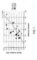
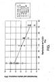
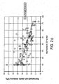
- the properties of each film are provided in Table V. Examples 9 through 11 reconfirm the array results of the effect of the carboxylate, the weight percent EO, and the pAcid values of the mixture have on the normalized wall elastic modulus.
Landscapes
- Chemical & Material Sciences (AREA)
- Engineering & Computer Science (AREA)
- Materials Engineering (AREA)
- Organic Chemistry (AREA)
- Formation Of Insulating Films (AREA)
- Internal Circuitry In Semiconductor Integrated Circuit Devices (AREA)
- Inorganic Insulating Materials (AREA)
- Silicon Compounds (AREA)
- Compositions Of Macromolecular Compounds (AREA)
- Laminated Bodies (AREA)
- Compositions Of Oxide Ceramics (AREA)
- Paints Or Removers (AREA)
- Manufacture Of Macromolecular Shaped Articles (AREA)
Priority Applications (1)
| Application Number | Priority Date | Filing Date | Title |
|---|---|---|---|
| EP07109359A EP1852903A3 (en) | 2002-05-30 | 2003-05-30 | Compositions for preparing materials with a low dielectric constant |
Applications Claiming Priority (4)
| Application Number | Priority Date | Filing Date | Title |
|---|---|---|---|
| US38432102P | 2002-05-30 | 2002-05-30 | |
| US384321P | 2002-05-30 | ||
| US638942 | 2003-05-20 | ||
| US10/638,942 US7122880B2 (en) | 2002-05-30 | 2003-05-20 | Compositions for preparing low dielectric materials |
Related Child Applications (1)
| Application Number | Title | Priority Date | Filing Date |
|---|---|---|---|
| EP07109359A Division EP1852903A3 (en) | 2002-05-30 | 2003-05-30 | Compositions for preparing materials with a low dielectric constant |
Publications (2)
| Publication Number | Publication Date |
|---|---|
| EP1376671A1 EP1376671A1 (en) | 2004-01-02 |
| EP1376671B1 true EP1376671B1 (en) | 2007-06-20 |
Family
ID=29718525
Family Applications (2)
| Application Number | Title | Priority Date | Filing Date |
|---|---|---|---|
| EP03012119A Expired - Lifetime EP1376671B1 (en) | 2002-05-30 | 2003-05-30 | Compositions for preparing materials with a low dielectric constant |
| EP07109359A Withdrawn EP1852903A3 (en) | 2002-05-30 | 2003-05-30 | Compositions for preparing materials with a low dielectric constant |
Family Applications After (1)
| Application Number | Title | Priority Date | Filing Date |
|---|---|---|---|
| EP07109359A Withdrawn EP1852903A3 (en) | 2002-05-30 | 2003-05-30 | Compositions for preparing materials with a low dielectric constant |
Country Status (10)
| Country | Link |
|---|---|
| US (3) | US7122880B2 (OSRAM) |
| EP (2) | EP1376671B1 (OSRAM) |
| JP (2) | JP2004161601A (OSRAM) |
| KR (1) | KR100561884B1 (OSRAM) |
| CN (1) | CN100539037C (OSRAM) |
| AT (1) | ATE365376T1 (OSRAM) |
| DE (1) | DE60314475T2 (OSRAM) |
| IL (2) | IL156231A (OSRAM) |
| SG (1) | SG110057A1 (OSRAM) |
| TW (2) | TWI303834B (OSRAM) |
Cited By (3)
| Publication number | Priority date | Publication date | Assignee | Title |
|---|---|---|---|---|
| US8557877B2 (en) | 2009-06-10 | 2013-10-15 | Honeywell International Inc. | Anti-reflective coatings for optically transparent substrates |
| US8864898B2 (en) | 2011-05-31 | 2014-10-21 | Honeywell International Inc. | Coating formulations for optical elements |
| US10544329B2 (en) | 2015-04-13 | 2020-01-28 | Honeywell International Inc. | Polysiloxane formulations and coatings for optoelectronic applications |
Families Citing this family (51)
| Publication number | Priority date | Publication date | Assignee | Title |
|---|---|---|---|---|
| US6800571B2 (en) * | 1998-09-29 | 2004-10-05 | Applied Materials Inc. | CVD plasma assisted low dielectric constant films |
| US6541367B1 (en) * | 2000-01-18 | 2003-04-01 | Applied Materials, Inc. | Very low dielectric constant plasma-enhanced CVD films |
| US20030211244A1 (en) * | 2002-04-11 | 2003-11-13 | Applied Materials, Inc. | Reacting an organosilicon compound with an oxidizing gas to form an ultra low k dielectric |
| US6815373B2 (en) * | 2002-04-16 | 2004-11-09 | Applied Materials Inc. | Use of cyclic siloxanes for hardness improvement of low k dielectric films |
| US7122880B2 (en) * | 2002-05-30 | 2006-10-17 | Air Products And Chemicals, Inc. | Compositions for preparing low dielectric materials |
| US7307343B2 (en) * | 2002-05-30 | 2007-12-11 | Air Products And Chemicals, Inc. | Low dielectric materials and methods for making same |
| US6972217B1 (en) * | 2002-12-23 | 2005-12-06 | Lsi Logic Corporation | Low k polymer E-beam printable mechanical support |
| US6897163B2 (en) * | 2003-01-31 | 2005-05-24 | Applied Materials, Inc. | Method for depositing a low dielectric constant film |
| US7288292B2 (en) * | 2003-03-18 | 2007-10-30 | International Business Machines Corporation | Ultra low k (ULK) SiCOH film and method |
| US20050260420A1 (en) * | 2003-04-01 | 2005-11-24 | Collins Martha J | Low dielectric materials and methods for making same |
| US7462678B2 (en) * | 2003-09-25 | 2008-12-09 | Jsr Corporation | Film forming composition, process for producing film forming composition, insulating film forming material, process for forming film, and silica-based film |
| US8734906B2 (en) * | 2003-11-21 | 2014-05-27 | Brismat Inc. | Films and method of production thereof |
| WO2005049757A1 (en) * | 2003-11-21 | 2005-06-02 | The University Of Queensland | Silica films and method of production thereof |
| WO2005061566A1 (ja) * | 2003-12-22 | 2005-07-07 | Lion Corporation | ハイパーブランチポリマー及びその製造方法、並びに該ハイパーブランチポリマーを含有するレジスト組成物 |
| US20050196974A1 (en) * | 2004-03-02 | 2005-09-08 | Weigel Scott J. | Compositions for preparing low dielectric materials containing solvents |
| US7015061B2 (en) * | 2004-08-03 | 2006-03-21 | Honeywell International Inc. | Low temperature curable materials for optical applications |
| JP4650885B2 (ja) * | 2004-09-07 | 2011-03-16 | 株式会社神戸製鋼所 | 多孔質膜の形成方法及びその方法によって形成された多孔質膜 |
| US7387973B2 (en) * | 2004-09-30 | 2008-06-17 | Taiwan Semiconductor Manufacturing Co., Ltd. | Method for improving low-K dielectrics by supercritical fluid treatments |
| KR101137812B1 (ko) * | 2004-12-20 | 2012-04-18 | 주식회사 동진쎄미켐 | 유기 반사방지막 형성용 유기 중합체 및 이를 포함하는유기 조성물 |
| US20070299176A1 (en) * | 2005-01-28 | 2007-12-27 | Markley Thomas J | Photodefinable low dielectric constant material and method for making and using same |
| US7867779B2 (en) | 2005-02-03 | 2011-01-11 | Air Products And Chemicals, Inc. | System and method comprising same for measurement and/or analysis of particles in gas stream |
| US20060183055A1 (en) * | 2005-02-15 | 2006-08-17 | O'neill Mark L | Method for defining a feature on a substrate |
| US7341788B2 (en) | 2005-03-11 | 2008-03-11 | International Business Machines Corporation | Materials having predefined morphologies and methods of formation thereof |
| US7425350B2 (en) * | 2005-04-29 | 2008-09-16 | Asm Japan K.K. | Apparatus, precursors and deposition methods for silicon-containing materials |
| EP1920023A4 (en) * | 2005-05-31 | 2009-08-19 | Xerocoat Inc | METHOD FOR TARGETING THE MORPHOLOGICAL RATIO OF SILICULATE ACID FILMS |
| JP4872246B2 (ja) * | 2005-06-10 | 2012-02-08 | 住友電気工業株式会社 | 半絶縁性GaAs基板及びエピタキシャル基板 |
| KR100725460B1 (ko) * | 2005-12-28 | 2007-06-07 | 삼성전자주식회사 | 금속 오염 분석용 표준 시료의 제조 방법 |
| JP4949692B2 (ja) * | 2006-02-07 | 2012-06-13 | 東京応化工業株式会社 | 低屈折率シリカ系被膜形成用組成物 |
| US20070196773A1 (en) * | 2006-02-22 | 2007-08-23 | Weigel Scott J | Top coat for lithography processes |
| US8399349B2 (en) | 2006-04-18 | 2013-03-19 | Air Products And Chemicals, Inc. | Materials and methods of forming controlled void |
| US20080012074A1 (en) * | 2006-07-14 | 2008-01-17 | Air Products And Chemicals, Inc. | Low Temperature Sol-Gel Silicates As Dielectrics or Planarization Layers For Thin Film Transistors |
| US7410916B2 (en) * | 2006-11-21 | 2008-08-12 | Applied Materials, Inc. | Method of improving initiation layer for low-k dielectric film by digital liquid flow meter |
| WO2008156680A1 (en) * | 2007-06-15 | 2008-12-24 | Sba Materials, Inc. | Low k dielectric |
| US7998536B2 (en) | 2007-07-12 | 2011-08-16 | Applied Materials, Inc. | Silicon precursors to make ultra low-K films of K<2.2 with high mechanical properties by plasma enhanced chemical vapor deposition |
| US7989033B2 (en) * | 2007-07-12 | 2011-08-02 | Applied Materials, Inc. | Silicon precursors to make ultra low-K films with high mechanical properties by plasma enhanced chemical vapor deposition |
| US20090093135A1 (en) * | 2007-10-04 | 2009-04-09 | Asm Japan K.K. | Semiconductor manufacturing apparatus and method for curing material with uv light |
| US8987039B2 (en) | 2007-10-12 | 2015-03-24 | Air Products And Chemicals, Inc. | Antireflective coatings for photovoltaic applications |
| US20090096106A1 (en) * | 2007-10-12 | 2009-04-16 | Air Products And Chemicals, Inc. | Antireflective coatings |
| KR101220029B1 (ko) * | 2008-04-02 | 2013-01-21 | 미쓰이 가가쿠 가부시키가이샤 | 조성물 및 그 제조 방법, 다공질 재료 및 그 형성 방법, 층간 절연막, 반도체 재료, 반도체 장치, 및 저굴절률 표면 보호막 |
| US20100151206A1 (en) | 2008-12-11 | 2010-06-17 | Air Products And Chemicals, Inc. | Method for Removal of Carbon From An Organosilicate Material |
| JP5708191B2 (ja) * | 2010-05-19 | 2015-04-30 | セントラル硝子株式会社 | 保護膜形成用薬液 |
| TWI413185B (zh) * | 2010-08-19 | 2013-10-21 | 國立交通大學 | 一種形成鍺半導體表面保護層的方法 |
| TWI410087B (zh) | 2010-12-20 | 2013-09-21 | Ind Tech Res Inst | 多核心晶片網路 |
| US20120237676A1 (en) * | 2011-03-14 | 2012-09-20 | Intermolecular, Inc. | Sol-gel based formulations and methods for preparation of hydrophobic ultra low refractive index anti-reflective coatings on glass |
| CN104823265A (zh) | 2012-10-31 | 2015-08-05 | Sba材料有限公司 | 含有非金属催化剂的低k介电溶胶的组合物 |
| DE102013107240A1 (de) * | 2013-07-09 | 2015-01-15 | Institut Für Verbundwerkstoffe Gmbh | Gemisch zur Herstellung von Nanopartikeln aus Siliziumdioxid, Verwendung eines solchen Gemisches, Verfahren zur Herstellung von Nanopartikeln aus Siliziumdioxid, Verwendung von nach dem Verfahren hergestellten Nanopartikeln aus Siliziumdioxid sowie nach dem Verfahren hergestellte Nanopartikel aus Siliziumdioxid |
| US9773698B2 (en) | 2015-09-30 | 2017-09-26 | International Business Machines Corporation | Method of manufacturing an ultra low dielectric layer |
| US20190134663A1 (en) * | 2017-10-27 | 2019-05-09 | Versum Materials Us, Llc | Silacyclic Compounds and Methods for Depositing Silicon-Containing Films Using Same |
| KR102267504B1 (ko) | 2017-12-22 | 2021-06-21 | 주식회사 엘지화학 | 메조포러스 실리카 코팅층을 포함하는 광학 부재의 제조방법 및 이를 이용하여 제조된 광학 부재 |
| US11158498B2 (en) * | 2018-06-19 | 2021-10-26 | Versum Materials Us, Llc | Silicon compounds and methods for depositing films using same |
| CN110330235B (zh) * | 2019-06-11 | 2021-10-01 | 惠科股份有限公司 | 多孔二氧化硅薄膜及其制备方法、以及显示面板 |
Citations (1)
| Publication number | Priority date | Publication date | Assignee | Title |
|---|---|---|---|---|
| EP1369907A2 (en) * | 2002-05-30 | 2003-12-10 | Air Products And Chemicals, Inc. | Low dielectric materials and methods for making same |
Family Cites Families (29)
| Publication number | Priority date | Publication date | Assignee | Title |
|---|---|---|---|---|
| US189495A (en) * | 1877-04-10 | Improvement in piles for nail-plates | ||
| US42210A (en) * | 1864-04-05 | Apparatus for upsetting tires | ||
| US5206091A (en) | 1988-06-28 | 1993-04-27 | Amoco Corporation | Low dielectric constant, low moisture uptake polyimides and copolyimides for interlevel dielectrics and substrate coatings |
| US5268193A (en) | 1988-06-28 | 1993-12-07 | Amoco Corporation | Low dielectric constant, low moisture uptake polyimides and copolyimides for interlevel dielectrics and substrate coatings |
| JPH09143420A (ja) | 1995-09-21 | 1997-06-03 | Asahi Glass Co Ltd | 低誘電率樹脂組成物 |
| US6126733A (en) | 1997-10-31 | 2000-10-03 | Alliedsignal Inc. | Alcohol based precursors for producing nanoporous silica thin films |
| DK199800404U3 (da) | 1998-10-28 | 1999-07-09 | Joergen Holberg Fenger | CD - system |
| US6329017B1 (en) | 1998-12-23 | 2001-12-11 | Battelle Memorial Institute | Mesoporous silica film from a solution containing a surfactant and methods of making same |
| IL143589A0 (en) * | 1998-12-23 | 2002-04-21 | Battelle Memorial Institute | Mesoporous silica film from a solution containing a surfactant and methods of making same |
| EP1058274B1 (en) | 1999-06-04 | 2005-07-27 | JSR Corporation | Composition for film formation and material for insulating film formation |
| US6495478B1 (en) * | 1999-06-21 | 2002-12-17 | Taiwan Semiconductor Manufacturing Company | Reduction of shrinkage of poly(arylene ether) for low-K IMD |
| JP2001048977A (ja) * | 1999-08-12 | 2001-02-20 | Jsr Corp | ポリアルキレンオキサイド誘導体の精製方法、膜形成用組成物、膜形成方法および低密度膜 |
| US6410151B1 (en) | 1999-09-29 | 2002-06-25 | Jsr Corporation | Composition for film formation, method of film formation, and insulating film |
| US6410150B1 (en) | 1999-09-29 | 2002-06-25 | Jsr Corporation | Composition for film formation, method of film formation, and insulating film |
| US6592980B1 (en) | 1999-12-07 | 2003-07-15 | Air Products And Chemicals, Inc. | Mesoporous films having reduced dielectric constants |
| US6365266B1 (en) * | 1999-12-07 | 2002-04-02 | Air Products And Chemicals, Inc. | Mesoporous films having reduced dielectric constants |
| KR100677782B1 (ko) | 2000-01-17 | 2007-02-05 | 제이에스알 가부시끼가이샤 | 절연막 형성용 재료의 제조 방법 |
| DE60138327D1 (de) | 2000-02-28 | 2009-05-28 | Jsr Corp | Zusammensetzung zur Filmerzeugung, Verfahren zur Filmerzeugung und Filme auf Basis von Siliciumoxid |
| US6576568B2 (en) | 2000-04-04 | 2003-06-10 | Applied Materials, Inc. | Ionic additives for extreme low dielectric constant chemical formulations |
| JP2001287910A (ja) * | 2000-04-04 | 2001-10-16 | Asahi Kasei Corp | 多孔質ケイ素酸化物塗膜の製造方法 |
| US6559070B1 (en) * | 2000-04-11 | 2003-05-06 | Applied Materials, Inc. | Mesoporous silica films with mobile ion gettering and accelerated processing |
| US6495479B1 (en) | 2000-05-05 | 2002-12-17 | Honeywell International, Inc. | Simplified method to produce nanoporous silicon-based films |
| TW452920B (en) | 2000-05-12 | 2001-09-01 | Taiwan Semiconductor Mfg | Method for forming low dielectric constant material |
| TW588072B (en) | 2000-10-10 | 2004-05-21 | Shipley Co Llc | Antireflective porogens |
| TW471108B (en) | 2000-11-27 | 2002-01-01 | Shr Min | Preparation of ultra low dielectric constant silicon dioxide film with nanometer pores |
| US6406794B1 (en) | 2001-02-08 | 2002-06-18 | Jsr Corporation | Film-forming composition |
| JP2002285086A (ja) | 2001-03-26 | 2002-10-03 | Jsr Corp | 膜形成用組成物、膜の形成方法およびシリカ系膜 |
| KR100432152B1 (ko) | 2001-04-12 | 2004-05-17 | 한국화학연구원 | 다분지형 폴리알킬렌 옥시드 포로젠과 이를 이용한저유전성 절연막 |
| US7122880B2 (en) * | 2002-05-30 | 2006-10-17 | Air Products And Chemicals, Inc. | Compositions for preparing low dielectric materials |
-
2003
- 2003-05-20 US US10/638,942 patent/US7122880B2/en not_active Expired - Fee Related
- 2003-05-30 TW TW095102894A patent/TWI303834B/zh not_active IP Right Cessation
- 2003-05-30 CN CNB031382975A patent/CN100539037C/zh not_active Expired - Fee Related
- 2003-05-30 DE DE60314475T patent/DE60314475T2/de not_active Expired - Lifetime
- 2003-05-30 JP JP2003154737A patent/JP2004161601A/ja active Pending
- 2003-05-30 SG SG200303511A patent/SG110057A1/en unknown
- 2003-05-30 TW TW092114842A patent/TWI265531B/zh not_active IP Right Cessation
- 2003-05-30 EP EP03012119A patent/EP1376671B1/en not_active Expired - Lifetime
- 2003-05-30 EP EP07109359A patent/EP1852903A3/en not_active Withdrawn
- 2003-05-30 AT AT03012119T patent/ATE365376T1/de not_active IP Right Cessation
- 2003-05-30 KR KR1020030034779A patent/KR100561884B1/ko not_active Expired - Fee Related
- 2003-06-01 IL IL156231A patent/IL156231A/en not_active IP Right Cessation
- 2003-06-01 IL IL188790A patent/IL188790A0/en unknown
-
2006
- 2006-07-11 US US11/484,075 patent/US7482676B2/en not_active Expired - Fee Related
- 2006-07-11 US US11/484,049 patent/US7294585B2/en not_active Expired - Fee Related
-
2010
- 2010-01-28 JP JP2010017150A patent/JP2010123992A/ja active Pending
Patent Citations (1)
| Publication number | Priority date | Publication date | Assignee | Title |
|---|---|---|---|---|
| EP1369907A2 (en) * | 2002-05-30 | 2003-12-10 | Air Products And Chemicals, Inc. | Low dielectric materials and methods for making same |
Cited By (4)
| Publication number | Priority date | Publication date | Assignee | Title |
|---|---|---|---|---|
| US8557877B2 (en) | 2009-06-10 | 2013-10-15 | Honeywell International Inc. | Anti-reflective coatings for optically transparent substrates |
| US8784985B2 (en) | 2009-06-10 | 2014-07-22 | Honeywell International Inc. | Anti-reflective coatings for optically transparent substrates |
| US8864898B2 (en) | 2011-05-31 | 2014-10-21 | Honeywell International Inc. | Coating formulations for optical elements |
| US10544329B2 (en) | 2015-04-13 | 2020-01-28 | Honeywell International Inc. | Polysiloxane formulations and coatings for optoelectronic applications |
Also Published As
| Publication number | Publication date |
|---|---|
| EP1852903A2 (en) | 2007-11-07 |
| SG110057A1 (en) | 2005-04-28 |
| EP1376671A1 (en) | 2004-01-02 |
| CN1487567A (zh) | 2004-04-07 |
| EP1852903A3 (en) | 2008-12-10 |
| JP2004161601A (ja) | 2004-06-10 |
| US20060249713A1 (en) | 2006-11-09 |
| US7482676B2 (en) | 2009-01-27 |
| DE60314475T2 (de) | 2008-02-28 |
| TW200703375A (en) | 2007-01-16 |
| TW200401310A (en) | 2004-01-16 |
| IL156231A0 (en) | 2004-01-04 |
| US7294585B2 (en) | 2007-11-13 |
| TWI265531B (en) | 2006-11-01 |
| IL156231A (en) | 2009-02-11 |
| US20060249818A1 (en) | 2006-11-09 |
| ATE365376T1 (de) | 2007-07-15 |
| TWI303834B (en) | 2008-12-01 |
| KR100561884B1 (ko) | 2006-03-17 |
| US20040048960A1 (en) | 2004-03-11 |
| CN100539037C (zh) | 2009-09-09 |
| IL188790A0 (en) | 2008-04-13 |
| KR20030094056A (ko) | 2003-12-11 |
| DE60314475D1 (de) | 2007-08-02 |
| JP2010123992A (ja) | 2010-06-03 |
| US7122880B2 (en) | 2006-10-17 |
Similar Documents
| Publication | Publication Date | Title |
|---|---|---|
| US7482676B2 (en) | Compositions for preparing low dielectric materials | |
| EP1832351B1 (en) | Low dielectric materials and methods for making same | |
| US7186613B2 (en) | Low dielectric materials and methods for making same | |
| US20090298671A1 (en) | Compositions for Preparing Low Dielectric Materials Containing Solvents | |
| EP1879234A2 (en) | Low temperature sol-gel silicates as dielectrics or planarization layers for thin film transistors | |
| KR100671860B1 (ko) | 규소 함유 잔류물을 기판으로부터 제거하기 위한 용매 및그 용매를 사용하여 규소 함유 잔류물을 기판으로부터 제거하는 방법 | |
| CN1757445B (zh) | 用于制备含溶剂的低介电材料的组合物 |
Legal Events
| Date | Code | Title | Description |
|---|---|---|---|
| PUAI | Public reference made under article 153(3) epc to a published international application that has entered the european phase |
Free format text: ORIGINAL CODE: 0009012 |
|
| AK | Designated contracting states |
Kind code of ref document: A1 Designated state(s): AT BE BG CH CY CZ DE DK EE ES FI FR GB GR HU IE IT LI LU MC NL PT RO SE SI SK TR |
|
| AX | Request for extension of the european patent |
Extension state: AL LT LV MK |
|
| RIN1 | Information on inventor provided before grant (corrected) |
Inventor name: WEIGEL, SCOTT JEFFREY Inventor name: PETERSON, BRIAN KEITH Inventor name: BRAYMER, THOMAS ALBERT Inventor name: CENDAK, KEITH Inventor name: CHONDROUDIS, KONSTANTINOS Inventor name: MACDOUGALL, JAMES EDWARD Inventor name: RAMBERG, C. ERIC Inventor name: CAMPBELL, KEITH DOUGLAS Inventor name: DEIS, DEIS, THOMAS ALLEN Inventor name: KIRNER, JOHN FRANCIS Inventor name: DEVENNEY, MARTIN |
|
| 17P | Request for examination filed |
Effective date: 20040129 |
|
| 17Q | First examination report despatched |
Effective date: 20040322 |
|
| AKX | Designation fees paid |
Designated state(s): AT BE BG CH CY CZ DE DK EE ES FI FR GB GR HU IE IT LI LU MC NL PT RO SE SI SK TR |
|
| GRAP | Despatch of communication of intention to grant a patent |
Free format text: ORIGINAL CODE: EPIDOSNIGR1 |
|
| GRAS | Grant fee paid |
Free format text: ORIGINAL CODE: EPIDOSNIGR3 |
|
| GRAA | (expected) grant |
Free format text: ORIGINAL CODE: 0009210 |
|
| AK | Designated contracting states |
Kind code of ref document: B1 Designated state(s): AT BE BG CH CY CZ DE DK EE ES FI FR GB GR HU IE IT LI LU MC NL PT RO SE SI SK TR |
|
| PG25 | Lapsed in a contracting state [announced via postgrant information from national office to epo] |
Ref country code: CH Free format text: LAPSE BECAUSE OF FAILURE TO SUBMIT A TRANSLATION OF THE DESCRIPTION OR TO PAY THE FEE WITHIN THE PRESCRIBED TIME-LIMIT Effective date: 20070620 Ref country code: LI Free format text: LAPSE BECAUSE OF FAILURE TO SUBMIT A TRANSLATION OF THE DESCRIPTION OR TO PAY THE FEE WITHIN THE PRESCRIBED TIME-LIMIT Effective date: 20070620 |
|
| REG | Reference to a national code |
Ref country code: GB Ref legal event code: FG4D |
|
| REG | Reference to a national code |
Ref country code: CH Ref legal event code: EP |
|
| REG | Reference to a national code |
Ref country code: IE Ref legal event code: FG4D |
|
| REF | Corresponds to: |
Ref document number: 60314475 Country of ref document: DE Date of ref document: 20070802 Kind code of ref document: P |
|
| PG25 | Lapsed in a contracting state [announced via postgrant information from national office to epo] |
Ref country code: SE Free format text: LAPSE BECAUSE OF FAILURE TO SUBMIT A TRANSLATION OF THE DESCRIPTION OR TO PAY THE FEE WITHIN THE PRESCRIBED TIME-LIMIT Effective date: 20070920 |
|
| ET | Fr: translation filed | ||
| PG25 | Lapsed in a contracting state [announced via postgrant information from national office to epo] |
Ref country code: AT Free format text: LAPSE BECAUSE OF FAILURE TO SUBMIT A TRANSLATION OF THE DESCRIPTION OR TO PAY THE FEE WITHIN THE PRESCRIBED TIME-LIMIT Effective date: 20070620 |
|
| REG | Reference to a national code |
Ref country code: CH Ref legal event code: PL |
|
| PG25 | Lapsed in a contracting state [announced via postgrant information from national office to epo] |
Ref country code: BE Free format text: LAPSE BECAUSE OF FAILURE TO SUBMIT A TRANSLATION OF THE DESCRIPTION OR TO PAY THE FEE WITHIN THE PRESCRIBED TIME-LIMIT Effective date: 20070620 |
|
| PG25 | Lapsed in a contracting state [announced via postgrant information from national office to epo] |
Ref country code: BG Free format text: LAPSE BECAUSE OF FAILURE TO SUBMIT A TRANSLATION OF THE DESCRIPTION OR TO PAY THE FEE WITHIN THE PRESCRIBED TIME-LIMIT Effective date: 20070920 Ref country code: PT Free format text: LAPSE BECAUSE OF FAILURE TO SUBMIT A TRANSLATION OF THE DESCRIPTION OR TO PAY THE FEE WITHIN THE PRESCRIBED TIME-LIMIT Effective date: 20071120 Ref country code: SI Free format text: LAPSE BECAUSE OF FAILURE TO SUBMIT A TRANSLATION OF THE DESCRIPTION OR TO PAY THE FEE WITHIN THE PRESCRIBED TIME-LIMIT Effective date: 20070620 Ref country code: CZ Free format text: LAPSE BECAUSE OF FAILURE TO SUBMIT A TRANSLATION OF THE DESCRIPTION OR TO PAY THE FEE WITHIN THE PRESCRIBED TIME-LIMIT Effective date: 20070620 Ref country code: ES Free format text: LAPSE BECAUSE OF FAILURE TO SUBMIT A TRANSLATION OF THE DESCRIPTION OR TO PAY THE FEE WITHIN THE PRESCRIBED TIME-LIMIT Effective date: 20071001 |
|
| PG25 | Lapsed in a contracting state [announced via postgrant information from national office to epo] |
Ref country code: SK Free format text: LAPSE BECAUSE OF FAILURE TO SUBMIT A TRANSLATION OF THE DESCRIPTION OR TO PAY THE FEE WITHIN THE PRESCRIBED TIME-LIMIT Effective date: 20070620 |
|
| PLBE | No opposition filed within time limit |
Free format text: ORIGINAL CODE: 0009261 |
|
| STAA | Information on the status of an ep patent application or granted ep patent |
Free format text: STATUS: NO OPPOSITION FILED WITHIN TIME LIMIT |
|
| PG25 | Lapsed in a contracting state [announced via postgrant information from national office to epo] |
Ref country code: GR Free format text: LAPSE BECAUSE OF FAILURE TO SUBMIT A TRANSLATION OF THE DESCRIPTION OR TO PAY THE FEE WITHIN THE PRESCRIBED TIME-LIMIT Effective date: 20070921 Ref country code: DK Free format text: LAPSE BECAUSE OF FAILURE TO SUBMIT A TRANSLATION OF THE DESCRIPTION OR TO PAY THE FEE WITHIN THE PRESCRIBED TIME-LIMIT Effective date: 20070620 |
|
| 26N | No opposition filed |
Effective date: 20080325 |
|
| PG25 | Lapsed in a contracting state [announced via postgrant information from national office to epo] |
Ref country code: RO Free format text: LAPSE BECAUSE OF FAILURE TO SUBMIT A TRANSLATION OF THE DESCRIPTION OR TO PAY THE FEE WITHIN THE PRESCRIBED TIME-LIMIT Effective date: 20070620 |
|
| PGFP | Annual fee paid to national office [announced via postgrant information from national office to epo] |
Ref country code: IT Payment date: 20080523 Year of fee payment: 6 |
|
| PGFP | Annual fee paid to national office [announced via postgrant information from national office to epo] |
Ref country code: NL Payment date: 20080410 Year of fee payment: 6 |
|
| PG25 | Lapsed in a contracting state [announced via postgrant information from national office to epo] |
Ref country code: MC Free format text: LAPSE BECAUSE OF NON-PAYMENT OF DUE FEES Effective date: 20080531 |
|
| PGFP | Annual fee paid to national office [announced via postgrant information from national office to epo] |
Ref country code: GB Payment date: 20080407 Year of fee payment: 6 |
|
| PG25 | Lapsed in a contracting state [announced via postgrant information from national office to epo] |
Ref country code: FI Free format text: LAPSE BECAUSE OF FAILURE TO SUBMIT A TRANSLATION OF THE DESCRIPTION OR TO PAY THE FEE WITHIN THE PRESCRIBED TIME-LIMIT Effective date: 20070620 |
|
| PG25 | Lapsed in a contracting state [announced via postgrant information from national office to epo] |
Ref country code: IE Free format text: LAPSE BECAUSE OF NON-PAYMENT OF DUE FEES Effective date: 20080530 Ref country code: EE Free format text: LAPSE BECAUSE OF FAILURE TO SUBMIT A TRANSLATION OF THE DESCRIPTION OR TO PAY THE FEE WITHIN THE PRESCRIBED TIME-LIMIT Effective date: 20070620 |
|
| PG25 | Lapsed in a contracting state [announced via postgrant information from national office to epo] |
Ref country code: CY Free format text: LAPSE BECAUSE OF FAILURE TO SUBMIT A TRANSLATION OF THE DESCRIPTION OR TO PAY THE FEE WITHIN THE PRESCRIBED TIME-LIMIT Effective date: 20070620 |
|
| GBPC | Gb: european patent ceased through non-payment of renewal fee |
Effective date: 20090530 |
|
| NLV4 | Nl: lapsed or anulled due to non-payment of the annual fee |
Effective date: 20091201 |
|
| PG25 | Lapsed in a contracting state [announced via postgrant information from national office to epo] |
Ref country code: NL Free format text: LAPSE BECAUSE OF NON-PAYMENT OF DUE FEES Effective date: 20091201 |
|
| PG25 | Lapsed in a contracting state [announced via postgrant information from national office to epo] |
Ref country code: GB Free format text: LAPSE BECAUSE OF NON-PAYMENT OF DUE FEES Effective date: 20090530 |
|
| PG25 | Lapsed in a contracting state [announced via postgrant information from national office to epo] |
Ref country code: LU Free format text: LAPSE BECAUSE OF NON-PAYMENT OF DUE FEES Effective date: 20080530 Ref country code: HU Free format text: LAPSE BECAUSE OF FAILURE TO SUBMIT A TRANSLATION OF THE DESCRIPTION OR TO PAY THE FEE WITHIN THE PRESCRIBED TIME-LIMIT Effective date: 20071221 |
|
| PGFP | Annual fee paid to national office [announced via postgrant information from national office to epo] |
Ref country code: FR Payment date: 20100525 Year of fee payment: 8 |
|
| PG25 | Lapsed in a contracting state [announced via postgrant information from national office to epo] |
Ref country code: TR Free format text: LAPSE BECAUSE OF FAILURE TO SUBMIT A TRANSLATION OF THE DESCRIPTION OR TO PAY THE FEE WITHIN THE PRESCRIBED TIME-LIMIT Effective date: 20070620 |
|
| PGFP | Annual fee paid to national office [announced via postgrant information from national office to epo] |
Ref country code: DE Payment date: 20100531 Year of fee payment: 8 |
|
| PG25 | Lapsed in a contracting state [announced via postgrant information from national office to epo] |
Ref country code: IT Free format text: LAPSE BECAUSE OF NON-PAYMENT OF DUE FEES Effective date: 20090530 |
|
| REG | Reference to a national code |
Ref country code: FR Ref legal event code: ST Effective date: 20120131 |
|
| REG | Reference to a national code |
Ref country code: DE Ref legal event code: R119 Ref document number: 60314475 Country of ref document: DE Effective date: 20111201 |
|
| PG25 | Lapsed in a contracting state [announced via postgrant information from national office to epo] |
Ref country code: FR Free format text: LAPSE BECAUSE OF NON-PAYMENT OF DUE FEES Effective date: 20110531 |
|
| PG25 | Lapsed in a contracting state [announced via postgrant information from national office to epo] |
Ref country code: DE Free format text: LAPSE BECAUSE OF NON-PAYMENT OF DUE FEES Effective date: 20111201 |