EP1369930B1 - Polymer Fasern und Bänder mit leitenden Partikel für Solarzellenelektroden - Google Patents
Polymer Fasern und Bänder mit leitenden Partikel für Solarzellenelektroden Download PDFInfo
- Publication number
- EP1369930B1 EP1369930B1 EP03010885A EP03010885A EP1369930B1 EP 1369930 B1 EP1369930 B1 EP 1369930B1 EP 03010885 A EP03010885 A EP 03010885A EP 03010885 A EP03010885 A EP 03010885A EP 1369930 B1 EP1369930 B1 EP 1369930B1
- Authority
- EP
- European Patent Office
- Prior art keywords
- fibers
- fiber
- solar cell
- ribbon
- inorganic material
- Prior art date
- Legal status (The legal status is an assumption and is not a legal conclusion. Google has not performed a legal analysis and makes no representation as to the accuracy of the status listed.)
- Expired - Lifetime
Links
Images
Classifications
-
- H—ELECTRICITY
- H01—ELECTRIC ELEMENTS
- H01B—CABLES; CONDUCTORS; INSULATORS; SELECTION OF MATERIALS FOR THEIR CONDUCTIVE, INSULATING OR DIELECTRIC PROPERTIES
- H01B1/00—Conductors or conductive bodies characterised by the conductive materials; Selection of materials as conductors
- H01B1/20—Conductive material dispersed in non-conductive organic material
- H01B1/22—Conductive material dispersed in non-conductive organic material the conductive material comprising metals or alloys
-
- H—ELECTRICITY
- H10—SEMICONDUCTOR DEVICES; ELECTRIC SOLID-STATE DEVICES NOT OTHERWISE PROVIDED FOR
- H10F—INORGANIC SEMICONDUCTOR DEVICES SENSITIVE TO INFRARED RADIATION, LIGHT, ELECTROMAGNETIC RADIATION OF SHORTER WAVELENGTH OR CORPUSCULAR RADIATION
- H10F10/00—Individual photovoltaic cells, e.g. solar cells
-
- B—PERFORMING OPERATIONS; TRANSPORTING
- B22—CASTING; POWDER METALLURGY
- B22F—WORKING METALLIC POWDER; MANUFACTURE OF ARTICLES FROM METALLIC POWDER; MAKING METALLIC POWDER; APPARATUS OR DEVICES SPECIALLY ADAPTED FOR METALLIC POWDER
- B22F1/00—Metallic powder; Treatment of metallic powder, e.g. to facilitate working or to improve properties
- B22F1/10—Metallic powder containing lubricating or binding agents; Metallic powder containing organic material
- B22F1/107—Metallic powder containing lubricating or binding agents; Metallic powder containing organic material containing organic material comprising solvents, e.g. for slip casting
-
- H—ELECTRICITY
- H10—SEMICONDUCTOR DEVICES; ELECTRIC SOLID-STATE DEVICES NOT OTHERWISE PROVIDED FOR
- H10F—INORGANIC SEMICONDUCTOR DEVICES SENSITIVE TO INFRARED RADIATION, LIGHT, ELECTROMAGNETIC RADIATION OF SHORTER WAVELENGTH OR CORPUSCULAR RADIATION
- H10F10/00—Individual photovoltaic cells, e.g. solar cells
- H10F10/10—Individual photovoltaic cells, e.g. solar cells having potential barriers
- H10F10/14—Photovoltaic cells having only PN homojunction potential barriers
-
- H—ELECTRICITY
- H10—SEMICONDUCTOR DEVICES; ELECTRIC SOLID-STATE DEVICES NOT OTHERWISE PROVIDED FOR
- H10F—INORGANIC SEMICONDUCTOR DEVICES SENSITIVE TO INFRARED RADIATION, LIGHT, ELECTROMAGNETIC RADIATION OF SHORTER WAVELENGTH OR CORPUSCULAR RADIATION
- H10F71/00—Manufacture or treatment of devices covered by this subclass
-
- H—ELECTRICITY
- H10—SEMICONDUCTOR DEVICES; ELECTRIC SOLID-STATE DEVICES NOT OTHERWISE PROVIDED FOR
- H10F—INORGANIC SEMICONDUCTOR DEVICES SENSITIVE TO INFRARED RADIATION, LIGHT, ELECTROMAGNETIC RADIATION OF SHORTER WAVELENGTH OR CORPUSCULAR RADIATION
- H10F77/00—Constructional details of devices covered by this subclass
- H10F77/20—Electrodes
- H10F77/206—Electrodes for devices having potential barriers
- H10F77/211—Electrodes for devices having potential barriers for photovoltaic cells
-
- B—PERFORMING OPERATIONS; TRANSPORTING
- B29—WORKING OF PLASTICS; WORKING OF SUBSTANCES IN A PLASTIC STATE IN GENERAL
- B29C—SHAPING OR JOINING OF PLASTICS; SHAPING OF MATERIAL IN A PLASTIC STATE, NOT OTHERWISE PROVIDED FOR; AFTER-TREATMENT OF THE SHAPED PRODUCTS, e.g. REPAIRING
- B29C48/00—Extrusion moulding, i.e. expressing the moulding material through a die or nozzle which imparts the desired form; Apparatus therefor
- B29C48/03—Extrusion moulding, i.e. expressing the moulding material through a die or nozzle which imparts the desired form; Apparatus therefor characterised by the shape of the extruded material at extrusion
- B29C48/05—Filamentary, e.g. strands
-
- B—PERFORMING OPERATIONS; TRANSPORTING
- B29—WORKING OF PLASTICS; WORKING OF SUBSTANCES IN A PLASTIC STATE IN GENERAL
- B29L—INDEXING SCHEME ASSOCIATED WITH SUBCLASS B29C, RELATING TO PARTICULAR ARTICLES
- B29L2031/00—Other particular articles
- B29L2031/731—Filamentary material, i.e. comprised of a single element, e.g. filaments, strands, threads, fibres
-
- Y—GENERAL TAGGING OF NEW TECHNOLOGICAL DEVELOPMENTS; GENERAL TAGGING OF CROSS-SECTIONAL TECHNOLOGIES SPANNING OVER SEVERAL SECTIONS OF THE IPC; TECHNICAL SUBJECTS COVERED BY FORMER USPC CROSS-REFERENCE ART COLLECTIONS [XRACs] AND DIGESTS
- Y02—TECHNOLOGIES OR APPLICATIONS FOR MITIGATION OR ADAPTATION AGAINST CLIMATE CHANGE
- Y02E—REDUCTION OF GREENHOUSE GAS [GHG] EMISSIONS, RELATED TO ENERGY GENERATION, TRANSMISSION OR DISTRIBUTION
- Y02E10/00—Energy generation through renewable energy sources
- Y02E10/50—Photovoltaic [PV] energy
- Y02E10/547—Monocrystalline silicon PV cells
Definitions
- This invention is directed to a process for the fabrication of features on solar cell structures utilizing fibers or ribbons comprising organic polymer and inorganic materials.
- a conventional solar cell structure with a p-type base has a negative electrode that is typically on the front side or sun side of the cell and a positive electrode on the backside.
- the solar cell has a carrier-collecting junction close to its front surface.
- the front surface is contacted with parallel fingers which are currently about 140 ⁇ m wide per finger.
- the fingers are connected by two bus bars that are perpendicular to the fingers.
- a five-inch square cell has about 55 fingers separated by about 2.1 mm spaces.
- the electric current collected for storage by the solar cell is gathered by metal contacts to a doped region on the front surface and by a second contact to the oppositely doped region on the back surface.
- the present invention will allow for the use of fibers or ribbons, wherein conductive metal particles are integrated into the fiber or ribbon, to form such electrodes on the front surface of the solar cell structure.
- the fibers or ribbons will allow narrower lines with increased height thickness which will increase the cell power by decreasing cell shadowing loss without increasing resistance of the lines.
- shadowing loss accounts for about 9% loss in a solar cell structure. Narrower lines will substantially decrease such loss.
- This invention provides a process for the manufacture of electrodes on a solar cell structure comprising the steps of affixing a fiber or ribbon comprising an organic polymer and a conductive inorganic material to a substrate such as a silicon wafer in a desired position forming a solar cell structure; heating the structure to a temperature above the melting point of the organic polymer; and heating the structure to a temperature to sufficiently effect the essentially complete removal of the organic polymer resulting in the conductive inorganic material being affixed to the substrate in the desired position.
- the present invention is directed to methods for the manufacture of solar cell structures utilizing fibers or ribbons bearing conductive metal particles combined with a spinnable fiber-forming dispersion.
- Examples of applications for the fibers or ribbons include the manufacture of features on a solar cell structure, for example, negative electrodes or emitters when the inorganic material of the fiber or ribbon are conductive metal particles.
- Polymers suitable for use in the present invention include those that form a spinnable dispersion with particles of inorganic materials such as conducting metal particles.
- the polymer must be soluble in a suitable solvent so that a dispersion comprising polymer and inorganic material particle can be prepared.
- the resulting inorganic material bearing polymer dispersion must be capable of being spun into flexible fibers or extruded into flexible ribbons.
- fiber means a single flexible filament; a group of flexible filaments twisted together or bundled together; or a group of flexible filaments lying parallel to each other forming a bundle. The bundle may or may not be coated to afford protection to the fiber.
- the fiber or bundle may be circular, oblong, square, rectangular, triangular and any other shape.
- ribbon means a flexible strip and may be one homogeneous ribbon; or may be constructed by laying more than one fiber in the same plane; or may be several homogeneous ribbons or planes of fibers or combinations thereof layered on top of one another to form a ribbon-like structure.
- fiber diameters typically range from 20 ⁇ m to 100 ⁇ m, but may extend beyond the range for some applications.
- Ribbon size typically ranges up to 200 ⁇ m ; in width to 100 ⁇ m in height but may extend beyond the range for some applications. Length of fiber or ribbon is preferred to be continuous, but noncontinuous fiber or ribbon lengths for forming components is suitable. Further, the polymer must be selected so as to soften and melt cleanly; for example, the polymer must bum out cleanly without leaving behind any residue. The polymer, in the presence of the inorganic material, must exhibit a melting point prior to decomposition. The polymer melt that results from the chosen polymer must wet out the material on which the solar cell is constructed.
- polymers examples include ethylene/vinyl acetate copolymers, obtainable from the DuPont Company (Wilmington, DE) under the trade name ELVAX®. Also, polymethylmethacrylate polymers may be suitable in the present invention and are available from the DuPont Company (Wilmington, DE) under the trade name ELVACITE®. Additional suitable ethylene/vinyl acetate copolymers and polymethylmethacrylate polymers are available from manufacturers such as Dow and Exxon.
- Organic solvents for use in the preparation of the spinnable inorganic material/polymer dispersion are characterized by high solubility for the polymer and by high vapor pressure at spinning temperatures to facilitate spinning of the inorganic material into polymer fiber or ribbon.
- suitable solvents include tetrachloroethylene, toluene, and xylenes. Dry spinning is a preferred technique for forming a fiber or ribbon. However, wet spinning, melt or gel spinning can be employed. All techniques are well known by those in the art of fiber technology.
- wet spinning is the oldest process. It is used for fiber-forming substances that have been dissolved in a solvent. The spinnerets are submerged in a chemical bath and as the filaments emerge they precipitate from solution and solidify. Because the solution is extruded directly into the precipitating liquid, this process for making fibers is called wet spinning.
- Dry spinning is also used for fiber-forming substances in solution.
- solidification is achieved by evaporating the solvent in a stream of air or inert gas. The filaments do not come in contact with a precipitating liquid, eliminating the need for drying and easing solvent recovery.
- melt spinning the fiber-forming substance is melted for extrusion through the spinneret and then directly solidified by cooling.
- Gel spinning is a special process used to obtain high strength or other special fiber properties.
- the polymer is not in a true liquid state during extrusion. Not completely separated, as they would be in a true solution, the polymer chains are bound together at various points in liquid crystal form. This produces strong inter-chain forces in the resulting filaments that can significantly increase the tensile strength of the fibers.
- the liquid crystals are aligned along the fiber axis by the shear forces during extrusion.
- the filaments emerge with an unusually high degree of orientation relative to each other, further enhancing strength.
- the process can also be described as dry-wet spinning, since the filaments first pass through air and then are cooled further in a liquid bath.
- Conductive metal materials in powder form usable in the process of the present invention are those known by those in the electronics industry.
- suitable conducting metals include those commonly used in solar devices, are as follows: Au, Ni, Au/Cr, Au/Cu, Au/Ta, Cu/Cr, Au/indium tin oxide, Cu, Ag and Ni. Ag is the preferred conducting metal.
- Fibers or ribbons comprising 70-80% conductive metal particles by weight are preferred; although, inorganic particle loading up to 90% by weight is suitable. Maximizing the inorganic solids loading will minimize shrinkage of the fibers during firing. However the polymer content must be kept high enough to form a flexible and uniform fiber or ribbon.
- the method of affixing the formed fiber or ribbon to the solar cell surface may be any method ranging from manual placement to mechanized placement means.
- the solar cell surface may be any surface suitable for use in solar cell manufacturing, but the preferred surfaces are processed Si wafers, CulnSe substrates, or substrates covered with thin films of amorphous silicon, CD-In-Ga-Se, CdS, ZnS, or CdTe.
- the first heating stage heats the solar cell structure that holds the affixed fiber or ribbon to a temperature above the melting point of the organic polymer component of the fiber or ribbon. This adheres the inorganic material/polymer fiber or ribbon to the substrate material.
- the heating source may be incorporated into a press plate. In another embodiment the heating source may be independent of the press plate.
- a second heating stage which substantially completely bums out the organic polymer from the fiber or ribbon results in the inorganic material adhering to the substrate material. It is preferred that the conductive inorganic materials are sintered.
- the firing temperature profile may be the two heating stages carried out in one continuum of heating or two discretely staged heating events.
- the fiber and/or ribbon placement and initial heating stage can be combined. Heating either the substrate and/or fiber/ribbon during the placement step can be used to secure the fiber/ribbon in the required position on the substrate. This would be the preferred positioning method to create functional features where there is no mechanical support structure to hold the fiber and/or ribbon in place. Another alternative method to tack fibers and/or ribbons in place without heating would be to wet the fiber or substrate surface with solvent vapors immediately before positioning (to make the fiber stick to the substrate).
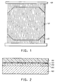
- Figure 1 illustrates a top surface metallization by the placement of multiple fine fibers (101) of conductive material onto a solar cell.
- the fibers are very narrow having dimensions of about 20 to 80 ⁇ m in width.
- the fibers can be extruded as either circular rods or rectangular shaped ribbon. Their aspect ratio may typically be about 1.
- the fibers may be placed by a fixture such as a loom (102) and positioned over the solar cell substrate such as a processed crystalline Si wafer (103). Proper positioning will need to be done accurately (X-Y positioning shown in Figure 1 ).
- X-Y positioning shown in Figure 1 A cross-sectional view of Figure 1 is shown in Figure 2.
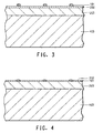
- Figure 2 positions the fibers close to the Si wafer surface prior to pressing with a heated TEFLON® plate (201).
- Fiber number and spacing will vary as a function of solar cell design. Some designs may have close spaces between lines as illustrated in Figure 1 . Some designs may have wider spaces between lines.
- the placement of fibers is a critical operation.
- the narrow fibers will need support, as they may be fragile. They will need to be positioned accurately with repeated performance.
- a press plate may both press and heat the fibers to stick them to the cell surface ( Figure 2 ).
- the TEFLON® plate will not grip the fibers thereby allowing the plate to be removed without pulling on the fibers. Prior to lifting the plate the fibers will typically be cut.
- an independent heating source may be used from the underside of the cell.
- the cell has a thin film antireflective coating of SiNx (202) on its upper surface. Under the SiNx is a diffused layer of n+Si (203)(typically Si with high concentration of P n-type dopant [for a negative emitter]). The base of the cell is p-type Si (103).
- Figure 3 shows the cell cross section of Figure 2 after the press plate is removed.
- the fibers (101) have been deformed slightly during pressing and heating and have been made to adhere to the top of the SiNx layer (202) (the outermost surface of the cell).
- Figure 4 illustrates the cell cross section of Figure 3 but after firing the fibers (101). The fibers contact the n+ Si layer (203) by penetrating the SiNx layer (202). This is necessary, as the SiNx is a non-conducting layer. Figure 4 also illustrates the fibers remaining in the same X-Y position after firing.
- a smooth fiber forming paste containing silver particles was made as follows. 5.0 g ELVAX® 265 ethylene vinyl acetate resin (DuPont, Wilmington, DE) was first soaked with 30 ml tetrachloroethylene (TCE) in a 100 ml beaker for one half hour. The beaker wrapped with a round band heater was enclosed in a bell jar. An air-driven stirrer was situated at the center of the bell jar for stirring the mixture in the beaker. The mixture was heated to 100°C until the polymer dissolved. To the solution, 15.0 g silver powder (silver powder, nominal size -2 ⁇ m D50 [-0.5 ⁇ m D10, -7 ⁇ m D90] available from E. I.
- du Pont de Nemours and Company, Wilmington, DE) and 0.4 g glass frit were added. It was stirred for about four hours. Once the mixture looked very smooth, vacuum was applied to the bell jar to thicken the mixture until an extensible viscosity was obtained. The mixture was then tested with a spatula to ascertain that fiber could be pulled from the smooth, thick paste. Once a smooth, fluid mixture was achieved, it was transferred to a plastic syringe having a - 0.5 mm diameter hypodermic needle for extrusion. The paste had to be kept at -80°C while it was being extruded to TEFLON® fluoropolymer sheets (DuPont, Wilmington, DE) for forming continuous fibers.
- TEFLON® fluoropolymer sheets DuPont, Wilmington, DE
- Fibers ranging from 100 to 300 ⁇ m were obtained.
- the obtained fibers were elastic and could be handled easily without breaking, which makes it possible for further processing.
- Thin ribbons down to 50 ⁇ m in thickness were obtained if the extrudates came into contact with the TEFLON® fluoropolymer sheets (DuPont, Wilmington, DE) before the skin of the extrudate had solidified.
- the silver fibers from Example 1 were affixed to a silicon wafer and fired at 900°C (set point) in an IR furnace. The fibers did not retain their original dimensions. The fired fibers measured 40 ⁇ m x 8 ⁇ m high.
Landscapes
- Physics & Mathematics (AREA)
- Chemical & Material Sciences (AREA)
- Dispersion Chemistry (AREA)
- Spectroscopy & Molecular Physics (AREA)
- Photovoltaic Devices (AREA)
- Non-Insulated Conductors (AREA)
Claims (6)
- Verfahren zum Bilden eines Streifens aus leitfähigem anorganischem Material auf ein Substrat zur Anwendung bei der Herstellung einer Solarzelle, umfassend die folgenden Schritte:a) Aufbringen einer Faser oder eines Bandes, umfassend ein organisches Polymer und ein leitfähiges anorganisches Material, in einer gewünschten Position auf ein Substrat, wobei ein Artikel gebildet wird; und dannb) Erhitzen des Artikels auf eine Temperatur, die ausreichend ist, um ein Entfernen des organischen Polymers zu bewirken, was zur Folge hat, dass das leitfähige anorganische Material in der gewünschten Position auf das Substrat aufgebracht wird.
- Verfahren nach Anspruch 1, ferner umfassend, vor Schritt a), Bilden der Faser oder des Bandes, umfassend das organische Polymer und das leitfähige anorganische Material.
- Verfahren nach Anspruch 1, wobei das leitfähige anorganische Material leitende Partikel ist, ausgewählt aus Au, Ni, Au/Cr, Au/Cu, Au/Ta, Cu/Cr, Au/Indiumzinnoxid, Cu, Ag und Ni.
- Verfahren nach Anspruch 2, wobei das Substrat eine Siliziumscheibe ist.
- Verfahren nach Anspruch 1, wobei Schritt a) das Erhitzen des Artikels auf eine Temperatur umfasst, die sich über dem Schmelzpunkt des organischen Polymers befindet.
- Verfahren nach Anspruch 1, wobei der Streifen aus leitfähigem anorganischem Material als Elektrode in einer Solarzellenstruktur verwendet wird.
Applications Claiming Priority (2)
| Application Number | Priority Date | Filing Date | Title |
|---|---|---|---|
| US38716002P | 2002-06-07 | 2002-06-07 | |
| US387160P | 2002-06-07 |
Publications (2)
| Publication Number | Publication Date |
|---|---|
| EP1369930A1 EP1369930A1 (de) | 2003-12-10 |
| EP1369930B1 true EP1369930B1 (de) | 2012-06-06 |
Family
ID=29550214
Family Applications (1)
| Application Number | Title | Priority Date | Filing Date |
|---|---|---|---|
| EP03010885A Expired - Lifetime EP1369930B1 (de) | 2002-06-07 | 2003-05-15 | Polymer Fasern und Bänder mit leitenden Partikel für Solarzellenelektroden |
Country Status (6)
| Country | Link |
|---|---|
| US (1) | US7163596B2 (de) |
| EP (1) | EP1369930B1 (de) |
| JP (2) | JP4122259B2 (de) |
| KR (1) | KR100568640B1 (de) |
| CN (1) | CN1471176B (de) |
| TW (1) | TWI249859B (de) |
Families Citing this family (8)
| Publication number | Priority date | Publication date | Assignee | Title |
|---|---|---|---|---|
| WO2002061791A2 (en) * | 2001-01-29 | 2002-08-08 | E. I. Du Pont De Nemours And Company | Fibers or ribbons for use in the manufacture of structures in flat panel display |
| US20050051207A1 (en) * | 2003-05-02 | 2005-03-10 | Carroll Alan F. | Fibers and ribbons for use in the manufacture of solar cells |
| US7618704B2 (en) * | 2003-09-29 | 2009-11-17 | E.I. Du Pont De Nemours And Company | Spin-printing of electronic and display components |
| US8143326B2 (en) * | 2004-09-28 | 2012-03-27 | E.I. Du Pont De Nemours And Company | Spin-printing of electronic and display components |
| US8252385B2 (en) * | 2005-03-25 | 2012-08-28 | E I Du Pont De Nemours And Company | Spin-printing of electronic and display components |
| KR101043927B1 (ko) * | 2008-10-23 | 2011-06-29 | 에스에스씨피 주식회사 | 태양 전지 및 그의 제조 방법 |
| KR101148031B1 (ko) * | 2010-08-11 | 2012-05-24 | 고려대학교 산학협력단 | 내부식성 태양전지 모듈 |
| FR2999804B1 (fr) * | 2012-12-18 | 2015-01-09 | Commissariat Energie Atomique | Dispositif d'interconnexion de cellules photovoltaiques a contacts en face arriere, et module comprenant un tel dispositif |
Family Cites Families (30)
| Publication number | Priority date | Publication date | Assignee | Title |
|---|---|---|---|---|
| US3492167A (en) | 1966-08-26 | 1970-01-27 | Matsushita Electric Industrial Co Ltd | Photovoltaic cell and method of making the same |
| US3666036A (en) * | 1970-05-18 | 1972-05-30 | Joseph Ernest Scerbo | Trailing road arm system |
| US3982964A (en) * | 1975-01-17 | 1976-09-28 | Communications Satellite Corporation (Comsat) | Dotted contact fine geometry solar cell |
| US4082568A (en) | 1977-05-10 | 1978-04-04 | Joseph Lindmayer | Solar cell with multiple-metal contacts |
| US4222977A (en) * | 1978-05-16 | 1980-09-16 | Monsanto Company | Process to produce inorganic hollow fibers |
| US4347762A (en) * | 1978-08-28 | 1982-09-07 | Borg-Warner Corporation | Planetary gear assembly |
| US4235644A (en) | 1979-08-31 | 1980-11-25 | E. I. Du Pont De Nemours And Company | Thick film silver metallizations for silicon solar cells |
| US4348458A (en) * | 1980-09-08 | 1982-09-07 | Monsanto Company | Coiled inorganic monolithic hollow fibers |
| US4347262A (en) | 1980-11-26 | 1982-08-31 | E. I. Du Pont De Nemours And Company | Aluminum-magnesium alloys in low resistance contacts to silicon |
| US4388346A (en) * | 1981-11-25 | 1983-06-14 | Beggs James M Administrator Of | Electrodes for solid state devices |
| JPS60140880A (ja) * | 1983-12-28 | 1985-07-25 | Hitachi Ltd | 太陽電池の製造方法 |
| JPS6199206A (ja) * | 1984-10-19 | 1986-05-17 | 住友電気工業株式会社 | 導電用材料 |
| US4826666A (en) | 1985-04-26 | 1989-05-02 | Sri International | Method of preparing metal carbides and the like and precursors used in such method |
| US4968738A (en) * | 1989-04-06 | 1990-11-06 | Quantum Materials, Inc. | Silver-glass die attach paste with reduced resin |
| KR910005090B1 (en) | 1989-06-02 | 1991-07-22 | Samsung Electronic Devices | Method of making the spacer of display device |
| EP0531827B1 (de) | 1991-08-30 | 1996-11-13 | Canon Kabushiki Kaisha | Solarzelle und deren Herstellungsmethode |
| JPH0563218A (ja) * | 1991-08-30 | 1993-03-12 | Canon Inc | 太陽電池及びその製造方法 |
| JP2596279B2 (ja) | 1992-01-30 | 1997-04-02 | 双葉電子工業株式会社 | 外囲器の支柱形成方法 |
| GB9224242D0 (en) | 1992-11-19 | 1993-01-06 | Rank Brimar Ltd | Preparation of metal or oxide films |
| JP3050064B2 (ja) * | 1994-11-24 | 2000-06-05 | 株式会社村田製作所 | 導電性ペースト、この導電性ペーストからなるグリッド電極が形成された太陽電池及びその製造方法 |
| US5674634A (en) | 1994-12-05 | 1997-10-07 | E. I. Du Pont De Nemours And Company | Insulator composition, green tape, and method for forming plasma display apparatus barrier-rib |
| US5714840A (en) | 1995-03-07 | 1998-02-03 | Asahi Glass Company Ltd. | Plasma display panel |
| US5723945A (en) | 1996-04-09 | 1998-03-03 | Electro Plasma, Inc. | Flat-panel display |
| JPH10149763A (ja) | 1996-11-18 | 1998-06-02 | Dainippon Printing Co Ltd | プラズマディスプレイパネル部材の製造方法 |
| US5851732A (en) | 1997-03-06 | 1998-12-22 | E. I. Du Pont De Nemours And Company | Plasma display panel device fabrication utilizing black electrode between substrate and conductor electrode |
| JP3686749B2 (ja) | 1997-11-04 | 2005-08-24 | 太陽インキ製造株式会社 | パターン状無機質焼成被膜及びプラズマディスプレイパネルの製造方法 |
| JP3877024B2 (ja) | 1998-04-13 | 2007-02-07 | 株式会社日立プラズマパテントライセンシング | プラズマディスプレイパネルの蛍光体層形成方法と装置並びにそれらに用いるフィラメント状成形体とその成形体の製造方法 |
| AU4370800A (en) | 1999-04-26 | 2000-11-10 | Chad Byron Moore | Fiber-based displays and methods for making same |
| JP2002094096A (ja) * | 2000-09-18 | 2002-03-29 | Canon Inc | 光起電力素子用集電電極の製造方法 |
| WO2002061791A2 (en) * | 2001-01-29 | 2002-08-08 | E. I. Du Pont De Nemours And Company | Fibers or ribbons for use in the manufacture of structures in flat panel display |
-
2003
- 2003-05-02 US US10/428,284 patent/US7163596B2/en not_active Expired - Fee Related
- 2003-05-15 EP EP03010885A patent/EP1369930B1/de not_active Expired - Lifetime
- 2003-05-16 TW TW092113359A patent/TWI249859B/zh not_active IP Right Cessation
- 2003-05-28 JP JP2003151559A patent/JP4122259B2/ja not_active Expired - Fee Related
- 2003-06-03 KR KR1020030035539A patent/KR100568640B1/ko not_active Expired - Fee Related
- 2003-06-06 CN CN031427472A patent/CN1471176B/zh not_active Expired - Fee Related
-
2006
- 2006-07-06 JP JP2006186943A patent/JP4726725B2/ja not_active Expired - Fee Related
Also Published As
| Publication number | Publication date |
|---|---|
| TW200406068A (en) | 2004-04-16 |
| CN1471176B (zh) | 2012-05-23 |
| EP1369930A1 (de) | 2003-12-10 |
| US20040009290A1 (en) | 2004-01-15 |
| CN1471176A (zh) | 2004-01-28 |
| TWI249859B (en) | 2006-02-21 |
| KR100568640B1 (ko) | 2006-04-07 |
| JP2004015054A (ja) | 2004-01-15 |
| JP2006279075A (ja) | 2006-10-12 |
| US7163596B2 (en) | 2007-01-16 |
| KR20030095243A (ko) | 2003-12-18 |
| JP4122259B2 (ja) | 2008-07-23 |
| JP4726725B2 (ja) | 2011-07-20 |
Similar Documents
| Publication | Publication Date | Title |
|---|---|---|
| EP1555695B1 (de) | Photovoltaisches Bauelement | |
| US20090146110A1 (en) | Fibers and ribbons for use in the manufacture of solar cells | |
| EP1369930B1 (de) | Polymer Fasern und Bänder mit leitenden Partikel für Solarzellenelektroden | |
| CN103718309B (zh) | 半导体基板及其制造方法、太阳能电池元件、以及太阳能电池 | |
| US20120282446A1 (en) | Carbon materials, product comprising the same, and method for preparing the same | |
| EP2462262A2 (de) | Grossflächige abscheidung von heteroepitaxial gezüchtetem graphen sowie produkte damit | |
| JP2001313400A (ja) | 太陽電池素子の形成方法 | |
| WO2013015329A1 (ja) | 配線部材及びその製造方法、並びに配線部材接着体の製造方法 | |
| KR20160034957A (ko) | 도전성 페이스트 및 결정계 실리콘 태양 전지의 제조 방법 | |
| CN107393623A (zh) | 用于太阳电池电极的组合物以及使用其制作的电极 | |
| EP1389342B1 (de) | Fasern oder bänder zur anwendung in der herstellung von strukturen in einem flachbildschirm | |
| JP2001127317A (ja) | 太陽電池の製造方法 | |
| KR101075185B1 (ko) | 다양한 크기와 형상을 갖는 막 구조체를 포함하는 소자 제조 방법 | |
| JP2004134656A (ja) | 太陽電池の製造方法およびその方法により製造した太陽電池 | |
| US5504015A (en) | Process for preparing photovoltaic modules based on crystalline silicon | |
| HK1060940A (en) | Fibers and ribbons for use in the manufacture of solar cells | |
| KR102861947B1 (ko) | 전도성 초박막의 제조 방법 및 그로부터 제조된 전도성 초박막 | |
| TW202000617A (zh) | 太陽能電池導電漿及其製造方法、以及高方阻太陽能電池電極的製造方法 | |
| JP2004095826A (ja) | 球状半導体素子の電極形成方法 | |
| JP2003017719A (ja) | 光電変換装置 | |
| JP2003163358A (ja) | 光電変換装置の製造方法 | |
| WO2015088312A1 (en) | A method for fabricating a thin-film solar cell having nanostructures incorporated onto an absorber layer and a conductor layer |
Legal Events
| Date | Code | Title | Description |
|---|---|---|---|
| PUAI | Public reference made under article 153(3) epc to a published international application that has entered the european phase |
Free format text: ORIGINAL CODE: 0009012 |
|
| AK | Designated contracting states |
Kind code of ref document: A1 Designated state(s): AT BE BG CH CY CZ DE DK EE ES FI FR GB GR HU IE IT LI LU MC NL PT RO SE SI SK TR |
|
| AX | Request for extension of the european patent |
Extension state: AL LT LV MK |
|
| 17P | Request for examination filed |
Effective date: 20040607 |
|
| AKX | Designation fees paid |
Designated state(s): DE FR GB |
|
| 17Q | First examination report despatched |
Effective date: 20071213 |
|
| GRAP | Despatch of communication of intention to grant a patent |
Free format text: ORIGINAL CODE: EPIDOSNIGR1 |
|
| GRAS | Grant fee paid |
Free format text: ORIGINAL CODE: EPIDOSNIGR3 |
|
| GRAA | (expected) grant |
Free format text: ORIGINAL CODE: 0009210 |
|
| AK | Designated contracting states |
Kind code of ref document: B1 Designated state(s): DE FR GB |
|
| REG | Reference to a national code |
Ref country code: GB Ref legal event code: FG4D |
|
| REG | Reference to a national code |
Ref country code: DE Ref legal event code: R096 Ref document number: 60341120 Country of ref document: DE Effective date: 20120809 |
|
| PLBE | No opposition filed within time limit |
Free format text: ORIGINAL CODE: 0009261 |
|
| STAA | Information on the status of an ep patent application or granted ep patent |
Free format text: STATUS: NO OPPOSITION FILED WITHIN TIME LIMIT |
|
| 26N | No opposition filed |
Effective date: 20130307 |
|
| REG | Reference to a national code |
Ref country code: DE Ref legal event code: R097 Ref document number: 60341120 Country of ref document: DE Effective date: 20130307 |
|
| GBPC | Gb: european patent ceased through non-payment of renewal fee |
Effective date: 20130515 |
|
| PG25 | Lapsed in a contracting state [announced via postgrant information from national office to epo] |
Ref country code: DE Free format text: LAPSE BECAUSE OF NON-PAYMENT OF DUE FEES Effective date: 20131203 |
|
| REG | Reference to a national code |
Ref country code: DE Ref legal event code: R119 Ref document number: 60341120 Country of ref document: DE Effective date: 20131203 |
|
| REG | Reference to a national code |
Ref country code: FR Ref legal event code: ST Effective date: 20140131 |
|
| PG25 | Lapsed in a contracting state [announced via postgrant information from national office to epo] |
Ref country code: GB Free format text: LAPSE BECAUSE OF NON-PAYMENT OF DUE FEES Effective date: 20130515 |
|
| PG25 | Lapsed in a contracting state [announced via postgrant information from national office to epo] |
Ref country code: FR Free format text: LAPSE BECAUSE OF NON-PAYMENT OF DUE FEES Effective date: 20130531 |