EP1363393A2 - Mischerschaltung - Google Patents
Mischerschaltung Download PDFInfo
- Publication number
- EP1363393A2 EP1363393A2 EP03010612A EP03010612A EP1363393A2 EP 1363393 A2 EP1363393 A2 EP 1363393A2 EP 03010612 A EP03010612 A EP 03010612A EP 03010612 A EP03010612 A EP 03010612A EP 1363393 A2 EP1363393 A2 EP 1363393A2
- Authority
- EP
- European Patent Office
- Prior art keywords
- transistor
- connection
- mixer circuit
- input
- input signal
- Prior art date
- Legal status (The legal status is an assumption and is not a legal conclusion. Google has not performed a legal analysis and makes no representation as to the accuracy of the status listed.)
- Withdrawn
Links
Images

Classifications
-
- H—ELECTRICITY
- H03—ELECTRONIC CIRCUITRY
- H03D—DEMODULATION OR TRANSFERENCE OF MODULATION FROM ONE CARRIER TO ANOTHER
- H03D7/00—Transference of modulation from one carrier to another, e.g. frequency-changing
- H03D7/14—Balanced arrangements
- H03D7/1425—Balanced arrangements with transistors
- H03D7/1441—Balanced arrangements with transistors using field-effect transistors
-
- H—ELECTRICITY
- H03—ELECTRONIC CIRCUITRY
- H03D—DEMODULATION OR TRANSFERENCE OF MODULATION FROM ONE CARRIER TO ANOTHER
- H03D7/00—Transference of modulation from one carrier to another, e.g. frequency-changing
- H03D7/14—Balanced arrangements
- H03D7/1425—Balanced arrangements with transistors
- H03D7/1433—Balanced arrangements with transistors using bipolar transistors
-
- H—ELECTRICITY
- H03—ELECTRONIC CIRCUITRY
- H03D—DEMODULATION OR TRANSFERENCE OF MODULATION FROM ONE CARRIER TO ANOTHER
- H03D7/00—Transference of modulation from one carrier to another, e.g. frequency-changing
- H03D7/14—Balanced arrangements
- H03D7/1425—Balanced arrangements with transistors
- H03D7/1458—Double balanced arrangements, i.e. where both input signals are differential
-
- H—ELECTRICITY
- H03—ELECTRONIC CIRCUITRY
- H03D—DEMODULATION OR TRANSFERENCE OF MODULATION FROM ONE CARRIER TO ANOTHER
- H03D2200/00—Indexing scheme relating to details of demodulation or transference of modulation from one carrier to another covered by H03D
- H03D2200/0041—Functional aspects of demodulators
- H03D2200/0043—Bias and operating point
Definitions
- the invention relates to a mixer circuit.
- a mixer circuit is mainly used in the Radio frequency technology, for example in an RF data transmission system, needed for frequency conversion.
- a high mixing gain and a low noise are all in one such case desirable to even small input signals to be able to reinforce to a sufficient extent.
- a known mixer circuit can be a passive one Mixer circuit with diodes or other passive Components.
- a known one Mixer circuit with an active mixer circuit Transistors can be a passive one Mixer circuit with diodes or other passive Components.
- a known one Mixer circuit with an active mixer circuit Transistors can be a known one Mixer circuit with an active mixer circuit Transistors.
- a known, very simple active mixer circuit is the additive mixer circuit , which is shown in Fig.1 .
- a first signal U e with a first frequency f e is input into the mixer circuit 101 via a first input 102.
- a second signal U 0 with a second frequency f 0 is input into the mixer circuit 101 via a second input 103.
- Mixed signals with different differential frequencies f mij , ie f m11
- , f m21
- , f m12
- the mixed signals are at the output 104 of the mixer circuit 101 issued.
- a known active mixer circuit which is widely used in applications, for example in data transmission, is the Gilbert cell named after Barrie Gilbert, the structure of which is illustrated in FIG .
- a mixer circuit 201 set up as a Gilbert cell has a signal input with a first signal connection RF 202 and a second signal connection RFN 203, one Local oscillator input with a first Local oscillator connection LO 204 and a second Local oscillator connection LON 205 and one Intermediate frequency output with a first Intermediate frequency connection ZF 206 and a second Intermediate frequency connection ZFN 207 on.
- the mixer circuit 201 also has an input subcircuit 214 with a first transistor 208 and a second transistor 209 and a local oscillator subcircuit 215 with a third transistor 216, a fourth Transistor 217, a fifth transistor 218 and one sixth transistor 219.
- the first transistor 208 and the second transistors 209 are at their emitter connections electrically coupled directly to each other.
- the collector connection of the first transistor 208 is connected to the emitter terminal of the fifth transistor 218 and with the emitter connection of the fourth transistor 217 electrically coupled.
- the collector connection of the second transistor 209 is connected the emitter connection of the third transistor 216 and with the Emitter connection of the sixth transistor 219 electrically coupled.
- the first signal connection RF 202 is with the basic connection 210 of the first transistor 208 is electrically coupled.
- the second signal connector RF 203 is connected to the base connector 211 of the second transistor 209 is electrically coupled.
- the first local oscillator connection LO 204 is with the base connection of the third transistor 216 and with the base terminal of the fifth transistor 218 is electrically coupled.
- the second local oscillator connection LON 205 is with the Base connection of the fourth transistor 217 and with the Base connection of the sixth transistor 219 electrically coupled.
- the first intermediate frequency connection ZF 206 is with the Collector connection of the third transistor 216 and the Collector connection of the fourth transistor 217 electrically coupled.
- the second intermediate frequency connection is ZFN 207 with the collector terminal of the fifth transistor 218 and the collector terminal of the sixth transistor 219 electrically coupled.
- a first input resistor 212 is connected in parallel with the first signal connection RF 202, by means of which a bias voltage V bias can be applied to the base connection of the first transistor 208 in order to set the operating point of the first transistor 208.
- a second input resistor 213 is connected in parallel to the second signal connection RFN 203, by means of which the bias voltage V bias can be applied to the base connection of the second transistor 209 in order to set the operating point of the second transistor 209.
- Either a separate resistor or the internal resistance of a voltage source that provides the bias voltage V bias can be used as input resistor 212.
- Either a separate resistor or the internal resistance of a first voltage source 220, which provides the bias voltage V bias can be used as the input resistor 213.
- a high-frequency input signal V RF with a signal frequency f RF is , via the two signal connections RF 202 and RFN 203, depending on the polarity of the high-frequency input signal, the base connection 210 of the first transistor 208 and the base connection 211 of the second transistor 209 of the mixer circuit 201 fed.
- a local oscillator signal V LO with a local oscillator frequency f LO Via the two local oscillator connections LO 204 and LON 205, a local oscillator signal V LO with a local oscillator frequency f LO , depending on the polarity of the local oscillator signal, the base connection of the third transistor 216 and the base connection of the fifth transistor 218 or the base connection of the fourth transistor 217 and the base terminal of the sixth transistor 219 of the mixer circuit 201.
- a supply voltage V CC of is also applied to the collector connection of the third transistor 216 and to the collector connection of the fourth transistor 217, or to the collector connection of the fifth transistor 218 and to the collector connection of the sixth transistor 219 a second voltage source 221 is applied.
- a mixed signal U m generated which by means of the collector terminal of the third transistor 216 and by the collector terminal of the fourth transistor 217 on first intermediate frequency connection ZF 206 of the intermediate frequency output can be output and can be output by means of the collector connection of the fourth transistor 218 and by means of the collector connection of the sixth transistor 219 at the second intermediate frequency connection ZFN 207 of the intermediate frequency output.
- the logarithmic voltage ratio of the intermediate frequency signal V IF and the input signal V RF is referred to as the gain G of the mixer circuit for the intermediate frequency signal.
- the gain G of the mixer circuit depends on the frequency.
- the frequency working range is the frequency range in which the mixer circuit achieves a profit G sufficient for its meaningful operation.
- the (upper) 3dB cut-off frequency of the mixer circuit is the frequency at which the logarithmic voltage ratio between the output signal U m or V IF and the input signal V RF is -3dB, and gives an indication of the frequency working range.
- the gain G has a maximum value G max at a maximum frequency f max within the frequency working range.
- the frequency working range and the operating point, ie the maximum frequency f max can usually be set to a limited extent by the circuit layout.
- [2] describes a mixer circuit in which between a controlled connection of a first Input signal transistor and a controlled connection a low-pass filter of a second input signal transistor is switched.
- the low pass filter is used to suppress unwanted harmonic spectral components.
- a further mixer circuit is also described in [3] with a capacitive element as a replacement for a parasitic Inductance.
- the invention is based on the problem, a Mixer circuit specify a higher gain and one has a larger bandwidth.
- a mixer circuit for mixing an input signal with an input frequency and a local oscillator signal with a local oscillator frequency for generating an intermediate frequency signal with an intermediate frequency has a signal input to which the input signal can be applied, ie supplied to the mixer circuit, the signal input having a first signal connection and a second signal connection having.
- At least one first input signal transistor and one second input signal transistor are provided in an input subcircuit of the mixer circuit.
- Each input signal transistor has a control connection, in other words a control input and two controlled connections.
- the control input of the first input signal transistor is coupled to the first signal connection and the control input of the second input signal transistor is coupled to the second signal connection, so that the differential input signal, ie the high-frequency input signal V RF with a signal frequency f RF , connects the two control inputs of the input signal -Transistors can be supplied.
- the mixer circuit also has a local oscillator input for inputting the local oscillator signal into the mixer circuit and an intermediate frequency output for outputting the intermediate frequency signal.
- a capacitance for example a capacitor, is coupled between a first controlled connection of the first input signal transistor and a first controlled connection of the second input signal transistor.
- the capacity is thus controlled between the first two Connections of the input signal transistors of the input subcircuit the mixer circuit switched, the first controlled connections not with the transistors of the Local oscillator subcircuit of the mixer circuit coupled are, i.e. the first controlled ports are those controlled connections of the input signal transistors that on that facing away from the local oscillator subcircuit Side of the mixer circuit are arranged, preferably from View of the input subcircuit on the ground side.
- the second are controlled connections of the input signal transistors with the transistors of the local oscillator subcircuit coupled to mix the input signal with the Local oscillator signal.
- the mixer circuit according to the invention has one the mixer circuit described in [1] significantly increased 3 dB bandwidth and a higher mix gain. Also the Noise figure of the mixer circuit according to the invention significantly reduced compared to the known mixer circuit.
- the mixer circuit arrangement according to the invention also has the Advantage that they are simple, reliable and powerful is.
- the invention can be clearly seen in that the additional capacity between the first controlled Connections of the transistors of the input subcircuit together with inductive components Mixer circuit forms a resonance, causing the Mixed profit and the range will be increased and the Noise figure is reduced.
- Mixer circuit set up fully differential.
- the local oscillator input of the mixer circuit thus has a first local oscillator connection and a second Local oscillator connection on.
- the intermediate frequency output has a first according to this embodiment of the invention Intermediate frequency connection and a second Intermediate frequency connection on.
- a very inexpensive and easy to manufacture Mixer circuit results in an embodiment of the Mixer circuit as a Gilbert cell.
- the transistors are designed as bipolar transistors, in which case preferably the first input signal transistor and the second input signal transistor Are bipolar transistors.
- the control input of the first In this case, the input signal transistor is the base connection of the first input signal transistor and the The control input of the second input signal transistor is the Base connection of the second input signal transistor.
- the first controlled connection of the first input signal transistor in this case is the emitter connection of the first input signal transistor and the first controlled Connection of the second input signal transistor is in in this case the emitter connection of the second input signal transistor.
- the transistors can be used as pnp bipolar transistors or alternatively as npn bipolar transistors be designed.
- MOS field-effect transistors M etal- O xide- S emiconductor field effect transistors
- MOS field-effect transistors can be configured as n-channel MOS field-effect transistors or as p-channel MOS field-effect transistors.
- first input signal transistor and the second input signal transistor as MOS field effect transistors set up and the control input of the first input signal transistor is the gate terminal of the first input signal transistor.
- the control input of the second input signal transistor is the gate terminal of the second input signal transistor.
- the first controlled Connection of the first input signal transistor is in this If a first source / drain connection, preferably the Source connection, the first input signal transistor and the first controlled connection of the second input signal transistor in this case is a first source / drain connection, preferably the source connection, the second Input signal transistor.
- the mixer circuit is the Invention at least partially integrated as a monolithic Circuit formed, preferably based on silicon.
- the mixer circuit with its transistors and possibly other components as housed or unhoused Individual components are provided, for example on a circuit board with each other according to the desired functionality are soldered together.
- the mixer circuit arrangement can Example based at least in part on silicon, or them can at least partially on a compound semiconductor to Example with a III-V semiconductor such as GaAs, InP, InSb or one or more other known III-V semiconductors, or based on a II-VI semiconductor, or on SiGe.
- a III-V semiconductor such as GaAs, InP, InSb or one or more other known III-V semiconductors, or based on a II-VI semiconductor, or on SiGe.
- BiCMOS, CMOS or other known technologies are possible Technologies for realizing the circuit arrangement.
- a very fast mixer circuit results in the case that they are based at least in part on SiGe technology is realized.
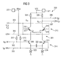
- FIG. 3 shows a sketch of a mixer circuit arrangement 300 according to a first exemplary embodiment of the invention.
- mixer circuit arrangement is one as a Gilbert cell provided mixer circuit provided.
- the mixer circuit arrangement 300 has a Gilbert cell as a mixer circuit 301 and a signal input with a first signal connection RF 302 and a second Signal connection RFN 303, a local oscillator input with a first local oscillator connection LO 304 and one second local oscillator connection LON 305 and one Intermediate frequency output with a first Intermediate frequency connection ZF 306 and a second Intermediate frequency connection ZFN 307.
- the mixer circuit 301 has an input subcircuit 314 with a first transistor 308 and a second Transistor 309 and a local oscillator subcircuit 315 with a third transistor 316, a fourth transistor 317, a fifth transistor 318 and a sixth transistor 319 on.
- the emitter connection of the first transistor 308 is connected coupled to a first terminal of a capacitance 322 whose second connection with the emitter connection of the second Transistor 309 is coupled.
- the first connection of the capacitance 322 is with a coupled first connection of a first current source 323, whose second connection is connected to ground potential is.
- the second connection of capacitance 322 is one coupled first connection of a second current source 324, their second connection also to the ground potential connected.
- the capacity 322 has according to this Embodiment a value of 1 pF.
- the collector connection of the first transistor 308 is connected the emitter terminal of the fifth transistor 318 and with the Emitter connection of the fourth transistor 317 electrically coupled.
- the collector connection of the second transistor 309 is with the emitter terminal of the third transistor 316 and with the emitter terminal of the sixth transistor 319 electrically coupled.
- the first RF 302 signal connector is with the base connector 310 of the first transistor 308 electrically coupled.
- the second signal connector RF 303 is with the base connector 311 of the second transistor 309 electrically coupled.
- the first local oscillator connection LO 304 is with the base connection of the third transistor 316 and with the base connection of fifth transistor 318 is electrically coupled.
- the second local oscillator connection LON 305 is with the Base connection of the fourth transistor 317 and with the Base connection of the sixth transistor 319 electrically coupled.
- the first intermediate frequency connection ZF 306 is with the Collector connection of the third transistor 316 and the Collector connection of the fourth transistor 317 electrically coupled.
- the second intermediate frequency connection is ZFN 307 with the collector terminal of the fifth transistor 318 and the collector terminal of the sixth transistor 319 electrically coupled.
- a first input resistor 312 is connected in parallel with the first signal connection RF 302, by means of which a bias voltage V bias can be applied to the base connection of the first transistor 308 in order to set the operating point of the first transistor 308.
- a second input resistor 313 is connected in parallel to the second signal connection RFN 303, by means of which the bias voltage V bias can be applied to the base connection of the second transistor 309 in order to set the operating point of the second transistor 309.
- the resistance value of the two input resistors 312 and 313 is 50 ohms each.
- the mixer circuit arrangement according to the invention is the Resistance value of the two input resistors 312 and 313 each 200 ohms, in another embodiment 300 ohms each.
- a high-frequency input signal V RF with a signal frequency f RF is sent to the base connection 310 of the first transistor 308 and the base connection 311 of the second transistor 309 of the mixer circuit 301 fed.
- a local oscillator signal V LO with a local oscillator frequency f LO Via the two local oscillator connections LO 304 and LON 305, a local oscillator signal V LO with a local oscillator frequency f LO , depending on the polarity of the local oscillator signal, the base connection of the third transistor 316 and the base connection of the fifth transistor 318 or the base connection of the fourth transistor 317 and the base terminal of the sixth transistor 319 of the mixer circuit 301.
- a supply voltage is also applied to the collector connection of the third transistor 316 and to the collector connection of the fourth transistor 317, or to the collector connection of the fifth transistor 318 and to the collector connection of the sixth transistor 319, via load resistors 325, 326 V CC applied from a second voltage source 321.
- a high-frequency input signal V RF and the local oscillator signal V LO are generated from the high-frequency input signal V m , which by means of the collector connection of the third transistor 316 and by means of the collector connection of the fourth transistor 317 am first intermediate frequency connection ZF 306 of the intermediate frequency output can be output and can be output by means of the collector connection of the fourth transistor 318 and by means of the collector connection of the sixth transistor 319 at the second intermediate frequency connection ZFN 307 of the intermediate frequency output.
- the Mixer circuit according to this embodiment stands out through a particularly high operating frequency.
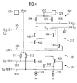
- FIG. 4 shows a sketch of a mixer circuit arrangement 400 according to a second exemplary embodiment of the invention.
- the mixer circuitry 400 according to the second Embodiment of the invention essentially corresponds the mixer circuit arrangement 300 according to the first Embodiment of the invention, which is why the same elements are provided with the same reference numerals in the figures.
- the mixer circuitry 400 according to the second Embodiment of the invention differs from that Mixer circuitry 300 according to the first Embodiment of the invention essentially in that the transistors of mixer circuit 401, i.e. the first Transistor 402, the second transistor 403, the third Transistor 404, fourth transistor 405, fifth Transistor 406 and the sixth transistor 407 as MOS field effect transistors are trained.
- the transistors of mixer circuit 401 i.e. the first Transistor 402, the second transistor 403, the third Transistor 404, fourth transistor 405, fifth Transistor 406 and the sixth transistor 407 as MOS field effect transistors are trained.
- the capacitance is 322 between the source terminals of the first transistor 402 and of the second transistor 403 coupled.
- the mixer circuit according to the invention is particularly suitable for use in signal processing at high carrier frequencies, for example with point-to-multipoint communication links 10.5 GHZ, at 24 GHz or at 26 GHz or with LMDS ( L ocal M ultipoint D istribution S ystem) at 28 GHz and 38 GHz and MVDS ( M ultipoint V ideo D istribution S ystems) at 42 GHz.
- LMDS L ocal M ultipoint D istribution S ystem
- MVDS M ultipoint V ideo D istribution S ystems
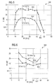
- FIG. 5 shows a diagram 500 in which the measured mixing gain G 501 as a function of the signal frequency RF 502 of the RF input signal in the case of a mixer circuit 301 configured as in FIG. 3 (as a first mixing gain curve 503) and the mixed gain G 501 in the case of a mixer circuit without the additional capacitance between the emitters of the transistors of the input subcircuit, with otherwise the same structure (as a second mixed gain curve 504), is shown.
- FIG. 6 shows a diagram 600 in which the measured double-sideband noise figure NF 601 as a function of the signal frequency RF 602 of the RF input signal in a mixer circuit 301 designed as shown in FIG. 3 (as a first noise figure curve 603) and the double-sideband noise figure NF 601 in the case of a mixer circuit without the additional capacitance between the emitters of the transistors of the input subcircuit, with an otherwise identical structure (as a second mixing gain curve 604).
- the invention can clearly be seen in that between the emitters of the transistor pair at the RF signal input a mixer, preferably one Gilbert mixer, an additional capacity is switched, by means of together with inductively acting components the mixer is resonated, whereby the Mixed gain and the 3 dB bandwidth is increased and the Noise figure is reduced.
- a mixer preferably one Gilbert mixer
Landscapes
- Engineering & Computer Science (AREA)
- Power Engineering (AREA)
- Superheterodyne Receivers (AREA)
- Amplifiers (AREA)
Abstract
Description
- Figur 1
- ein Schaltungsdiagramm einer additiven Mischerschaltung gemäß dem Stand der Technik;
- Figur 2
- ein Schaltungsdiagramm einer Gilbertzelle gemäß dem Stand der Technik;
- Figur 3
- ein Schaltungsdiagramm einer Mischerschaltung gemäß einem ersten Ausführungsbeispiel der Erfindung;
- Figur 4
- ein Schaltungsdiagramm einer Mischerschaltung gemäß einem zweiten Ausführungsbeispiel der Erfindung;
- Figur 5
- eine Skizze, in der der ermittelte Mischgewinn abhängig von der Signalfrequenz des Eingangssignals bei einer gemäß Figur 3 ausgestalteten Mischerschaltung und der Mischgewinn bei einer ansonsten strukturgleichen Mischerschaltung ohne die zusätzliche Kapazität zwischen den Emittern der Transistoren der Eingangs-Teilschaltung, dargestellt sind; und
- Figur 6
- eine Skizze, in der die ermittelte Zweiseitenband-Rauschzahl abhängig von der Signalfrequenz des Eingangssignals bei einer gemäß Figur 3 ausgestalteten Mischerschaltung und die Zweiseitenband-Rauschzahl bei einer ansonsten strukturgleichen Mischerschaltung ohne die zusätzliche Kapazität zwischen den Emittern der Transistoren der Eingangs-Teilschaltung, dargestellt sind.
- 101
- Mischerschaltung
- 102
- Erster Eingang
- 103
- Zweiter Eingang
- 104
- Ausgang
- 105
- Mischer-Transistor
- 106
- Basis
- 107
- Emitter
- 108
- Kollektor
- 201
- Mischerschaltung
- 202
- Erster Signalanschluss RF
- 203
- Zweiter Signalanschluss RFN
- 204
- Erster Lokaloszillatoranschluss LO
- 205
- Zweiter Lokaloszillatoranschluss LON
- 206
- Erster Zwischenfrequenzanschluss ZF
- 207
- Zweiter Zwischenfrequenzanschluss ZFN
- 208
- Erster Transistor
- 209
- Zweiter Transistor
- 210
- Basis des ersten Transistors
- 211
- Basis des zweiten Transistors
- 212
- Erster Eingangswiderstand
- 213
- Zweiter Eingangswiderstand
- 214
- Eingangsteilschaltung
- 215
- Lokaloszillatorteilschaltung
- 216
- Dritter Transistor
- 217
- Vierter Transistor
- 218
- Fünfter Transistor
- 219
- Sechster Transistor
- 220
- Erste Spannungsquelle
- 221
- Zweite Spannungsquelle
- 300
- Mischerschaltungsanordnung
- 301
- Mischerschaltung
- 302
- Erster Signalanschluss RF
- 303
- Zweiter Signalanschluss RFN
- 304
- Erster Lokaloszillatoranschluss LO
- 305
- Zweiter Lokaloszillatoranschluss LON
- 306
- Erster Zwischenfrequenzanschluss ZF
- 307
- Zweiter Zwischenfrequenzanschluss ZFN
- 308
- Erster Transistor
- 309
- Zweiter Transistor
- 310
- Basis-Anschluss des ersten Transistors
- 311
- Basis-Anschluss des zweiten Transistors
- 312
- Erster Eingangswiderstand
- 313
- Zweiter Eingangswiderstand
- 314
- Eingangs-Teilschaltung
- 315
- Lokaloszillatorteilschaltung
- 316
- Dritter Transistor
- 317
- Vierter Transistor
- 318
- Fünfter Transistor
- 319
- Sechster Transistor
- 320
- Erste Spannungsquelle
- 321
- Zweite Spannungsquelle
- 323
- Erste Stromquelle
- 324
- Zweite Stromquelle
- 325
- Lastwiderstand
- 326
- Lastwiderstand
- 400
- Mischerschaltungsanordnung
- 401
- Mischerschaltung
- 402
- Erster Transistor
- 403
- Zweiter Transistor
- 404
- Dritter Transistor
- 405
- Vierter Transistor
- 406
- Fünfter Transistor
- 407
- Sechster Transistor
- 500
- Diagramm
- 501
- Mischgewinn
- 502
- Frequenz
- 503
- Erste Mischgewinnkurve
- 504
- Zweite Mischgewinnkurve
- 600
- Diagramm
- 601
- Zweiseitenband-Rauschzahl
- 602
- Frequenz
- 603
- Erste Rauschzahlkurve
- 604
- Zweite Rauschzahlkurve
Claims (13)
- Mischerschaltung (201) zum Mischen eines Eingangssignals (VRF) mit einer Eingangsfrequenz (fRF) und eines Lokaloszillatorsignals (VLO) mit einer Lokaloszillatorfrequenz (fLO) zum Erzeugen eines Zwischenfrequenzsignals (ZF) mit einer Zwischenfrequenz (fZF),mit einem Signaleingang zum Eingeben des Eingangssignals (VRF), wobei der Signaleingang einen ersten Signalanschluss und einen zweiten Signalanschluss (RF 202, RFN 203) aufweist,mit einem ersten Eingangssignal-Transistor, dessen Steuereingang mit dem ersten Signalanschluss gekoppelt ist,mit einem zweiten Eingangssignal-Transistor, dessen Steuereingang mit dem zweiten Signalanschluss gekoppelt ist,mit einem Lokaloszillatoreingang zum Eingeben des Lokaloszillatorsignals (VLO) in die Mischerschaltung (201), undmit einem Zwischenfrequenzausgang zum Ausgeben des Zwischenfrequenzsignals (VZF),mit einer Kapazität zwischen einem ersten gesteuerten Anschluss des ersten Eingangssignal-Transistors und einem ersten gesteuerten Anschluss des zweiten Eingangssignal-Transistors.
- Mischerschaltung (201) nach Anspruch 1, bei derder Lokaloszillatoreingang einen ersten und einen zweiten Lokaloszillatoranschluss (LO 204, LON 205) aufweist, undder Zwischenfrequenzausgang einen ersten und einen zweiten Zwischenfrequenzanschluss (ZF 206, ZFN 207) aufweist.
- Mischerschaltung (201) nach Anspruch 1 oder 2, eingerichtet als eine Gilbertzelle.
- Mischerschaltung (201) nach einem der Ansprüche 1 bis 3, bei der zumindest ein Teil der Transistoren Bipolartransistoren sind.
- Mischerschaltung (201) nach Anspruch 4,bei der der erste Eingangssignal-Transistor und der zweite Eingangssignal-Transistor Bipolartransistoren sind,bei der der Steuereingang des ersten Eingangssignal-Transistors und des zweites Eingangssignal-Transistors jeweils deren Basis-Anschluss ist, undbei der der erste gesteuerten Anschluss des ersten Eingangssignal-Transistors und des zweiten Eingangssignal-Transistors jeweils deren Emitter-Anschluss ist.
- Mischerschaltung (201) nach einem der Ansprüche 1 bis 3, bei der zumindest ein Teil der Transistoren MOS-Feldeffekttransistoren sind.
- Mischerschaltung (201) nach Anspruch 6,bei der der erste Eingangssignal-Transistor und der zweite Eingangssignal-Transistor MOS-Feldeffekttransistoren sind,bei der der Steuereingang des ersten Eingangssignal-Transistors und des zweites Eingangssignal-Transistors jeweils deren Gate-Anschluss ist, undbei der der erste gesteuerten Anschluss des ersten Eingangssignal-Transistors und des zweiten Eingangssignal-Transistors jeweils deren Source-Anschluss ist.
- Mischerschaltung (201) nach einem der Ansprüche 1 bis 7, die zumindest teilweise als monolithisch integrierte Schaltung ausgebildet ist.
- Mischerschaltung (201) nach Anspruch 8, die zumindest teilweise auf Silizium basiert.
- Mischerschaltung (201) nach Anspruch 8, die zumindest teilweise auf zumindest einem Verbindungshalbleiter basiert.
- Mischerschaltung (201) nach Anspruch 9 oder 10, die zumindest teilweise auf BiCMOS-Technologie basiert.
- Mischerschaltung (201) nach Anspruch 9 oder 10, die zumindest teilweise auf CMOS-Technologie basiert.
- Mischerschaltung (201) nach Anspruch 9 oder 10, die zumindest teilweise auf SiGe-Technologie basiert.
Applications Claiming Priority (2)
| Application Number | Priority Date | Filing Date | Title |
|---|---|---|---|
| DE10221620 | 2002-05-15 | ||
| DE10221620 | 2002-05-15 |
Publications (2)
| Publication Number | Publication Date |
|---|---|
| EP1363393A2 true EP1363393A2 (de) | 2003-11-19 |
| EP1363393A3 EP1363393A3 (de) | 2003-12-10 |
Family
ID=29265307
Family Applications (1)
| Application Number | Title | Priority Date | Filing Date |
|---|---|---|---|
| EP03010612A Withdrawn EP1363393A3 (de) | 2002-05-15 | 2003-05-12 | Mischerschaltung |
Country Status (2)
| Country | Link |
|---|---|
| US (1) | US20040082307A1 (de) |
| EP (1) | EP1363393A3 (de) |
Families Citing this family (1)
| Publication number | Priority date | Publication date | Assignee | Title |
|---|---|---|---|---|
| WO2006077525A1 (en) * | 2005-01-21 | 2006-07-27 | Nxp B.V. | A high dynamic range low-power differential input stage |
Family Cites Families (9)
| Publication number | Priority date | Publication date | Assignee | Title |
|---|---|---|---|---|
| US5379457A (en) * | 1993-06-28 | 1995-01-03 | Hewlett-Packard Company | Low noise active mixer |
| US6026286A (en) * | 1995-08-24 | 2000-02-15 | Nortel Networks Corporation | RF amplifier, RF mixer and RF receiver |
| US5884154A (en) * | 1996-06-26 | 1999-03-16 | Raytheon Company | Low noise mixer circuit having passive inductor elements |
| JPH1056336A (ja) * | 1996-08-09 | 1998-02-24 | Mitsubishi Electric Corp | ミキサ回路 |
| US5847623A (en) * | 1997-09-08 | 1998-12-08 | Ericsson Inc. | Low noise Gilbert Multiplier Cells and quadrature modulators |
| US6037825A (en) * | 1997-11-04 | 2000-03-14 | Nortel Networks Corporation | Tree mixer operable in class A, B or AB |
| FR2791810B1 (fr) * | 1999-03-31 | 2001-06-22 | France Telecom | Procede de fabrication d'une heterostructure planaire |
| FI108584B (fi) * | 2000-03-24 | 2002-02-15 | Nokia Corp | Menetelmä välitaajuussignaalin muodostamiseksi sekoittimessa ja sekoitin |
| US6348830B1 (en) * | 2000-05-08 | 2002-02-19 | The Regents Of The University Of Michigan | Subharmonic double-balanced mixer |
-
2003
- 2003-05-12 EP EP03010612A patent/EP1363393A3/de not_active Withdrawn
- 2003-06-09 US US10/434,325 patent/US20040082307A1/en not_active Abandoned
Also Published As
| Publication number | Publication date |
|---|---|
| US20040082307A1 (en) | 2004-04-29 |
| EP1363393A3 (de) | 2003-12-10 |
Similar Documents
| Publication | Publication Date | Title |
|---|---|---|
| DE69426650T2 (de) | Mischer für Sender, mit einem Eingang im Strom-Modus | |
| DE19627640C2 (de) | Mischer | |
| DE69726058T2 (de) | Verstärkerschaltung und mehrstufige Verstärkerschaltung | |
| EP1067679B1 (de) | Differenzverstärker | |
| DE602004003145T2 (de) | Mischerschaltung, empfänger mit einer mischerschaltung, drahtlose kommunikationsvorrichtung mit einem empfänger, methode zur erzeugung eines ausgangssignals durch mischen eines eingangssignals mit einem oszillatorsignal | |
| DE602004008898T2 (de) | Funkempfänger-Eingangsstufe und Verfahren zur Unterdrückung von Aussenbandstörung | |
| DE102004063722A1 (de) | Schaltung zur Reduzierung von Intermodulation zweiter Ordnung und Direktwandlungsempfänger | |
| DE102008048986B4 (de) | Antennenverstärker und Empfangssystem | |
| DE102014103329A1 (de) | System und Verfahren für einen Frequenzverdoppler | |
| DE60133088T2 (de) | Eingangsstufe und hochfrequenzempfänger mit rauscharmem quadraturverstärker | |
| DE3782027T2 (de) | Elektronischer schalter fuer sehr hohe frequenzen. | |
| DE102014017291A1 (de) | Stromgesteuerte invertierende Transkonduktanzverstärker | |
| DE69214923T2 (de) | Integrierte Schaltung mit einem Verstärker mit variabler Verstärkung | |
| DE10344876B3 (de) | Signalverarbeitungseinrichtung, insbesondere für den Mobilfunk | |
| DE69613628T2 (de) | Eingangsschaltung | |
| DE102004030039B3 (de) | Mischerschaltung | |
| EP1405400B1 (de) | Schnittstellenschaltung zum anschluss an einen ausgang eines frequenzumsetzers | |
| EP1363393A2 (de) | Mischerschaltung | |
| DE102005037877A1 (de) | Diodenmischer | |
| EP0590191A1 (de) | Anordnung zur Frequenzumsetzung | |
| DE60018688T2 (de) | Verstärkungssteuerung für einen Verstärker | |
| DE69721898T2 (de) | Verstärker mit variabler Verstärkung und geringer Gleichspannungsabweichung am Ausgang und geringen Verzerrungen | |
| DE102005040489A1 (de) | Halbleiter-IC | |
| DE69519266T2 (de) | Mikrowellenmischerschaltung und diese Schaltung enthaltender Abwärtsumsetzer | |
| DE102004004609A1 (de) | Verstärker mit fester Eingangsimpedanz, betrieben in verschiedenen Verstärkungsmodi |
Legal Events
| Date | Code | Title | Description |
|---|---|---|---|
| PUAI | Public reference made under article 153(3) epc to a published international application that has entered the european phase |
Free format text: ORIGINAL CODE: 0009012 |
|
| PUAL | Search report despatched |
Free format text: ORIGINAL CODE: 0009013 |
|
| AK | Designated contracting states |
Kind code of ref document: A2 Designated state(s): AT BE BG CH CY CZ DE DK EE ES FI FR GB GR HU IE IT LI LU MC NL PT RO SE SI SK TR |
|
| AX | Request for extension of the european patent |
Extension state: AL LT LV MK |
|
| RIN1 | Information on inventor provided before grant (corrected) |
Inventor name: HACKL, SABINE |
|
| AK | Designated contracting states |
Kind code of ref document: A3 Designated state(s): AT BE BG CH CY CZ DE DK EE ES FI FR GB GR HU IE IT LI LU MC NL PT RO SE SI SK TR |
|
| AX | Request for extension of the european patent |
Extension state: AL LT LV MK |
|
| 17P | Request for examination filed |
Effective date: 20040121 |
|
| 17Q | First examination report despatched |
Effective date: 20040524 |
|
| AKX | Designation fees paid |
Designated state(s): DE FR GB |
|
| STAA | Information on the status of an ep patent application or granted ep patent |
Free format text: STATUS: THE APPLICATION IS DEEMED TO BE WITHDRAWN |
|
| 18D | Application deemed to be withdrawn |
Effective date: 20041204 |