EP1360515B1 - Method and apparatus for detection and measurement of accumulations of magnetic particles - Google Patents
Method and apparatus for detection and measurement of accumulations of magnetic particles Download PDFInfo
- Publication number
- EP1360515B1 EP1360515B1 EP02719038A EP02719038A EP1360515B1 EP 1360515 B1 EP1360515 B1 EP 1360515B1 EP 02719038 A EP02719038 A EP 02719038A EP 02719038 A EP02719038 A EP 02719038A EP 1360515 B1 EP1360515 B1 EP 1360515B1
- Authority
- EP
- European Patent Office
- Prior art keywords
- magnetic field
- magnetic
- excitation current
- sensing
- particles
- Prior art date
- Legal status (The legal status is an assumption and is not a legal conclusion. Google has not performed a legal analysis and makes no representation as to the accuracy of the status listed.)
- Expired - Lifetime
Links
- 238000000034 method Methods 0.000 title claims abstract description 35
- 239000006249 magnetic particle Substances 0.000 title claims abstract description 29
- 238000005259 measurement Methods 0.000 title claims abstract description 24
- 238000001514 detection method Methods 0.000 title abstract description 32
- 230000035508 accumulation Effects 0.000 title description 10
- 238000009825 accumulation Methods 0.000 title description 10
- 230000005291 magnetic effect Effects 0.000 claims abstract description 71
- 239000002245 particle Substances 0.000 claims abstract description 44
- 239000000758 substrate Substances 0.000 claims abstract description 27
- 230000004520 agglutination Effects 0.000 claims abstract 3
- 230000005284 excitation Effects 0.000 claims description 25
- 230000005415 magnetization Effects 0.000 claims description 19
- 230000008878 coupling Effects 0.000 claims description 3
- 238000010168 coupling process Methods 0.000 claims description 3
- 238000005859 coupling reaction Methods 0.000 claims description 3
- 239000004020 conductor Substances 0.000 claims 1
- 239000000463 material Substances 0.000 description 11
- XEEYBQQBJWHFJM-UHFFFAOYSA-N Iron Chemical compound [Fe] XEEYBQQBJWHFJM-UHFFFAOYSA-N 0.000 description 10
- 239000003446 ligand Substances 0.000 description 9
- 239000011324 bead Substances 0.000 description 8
- 238000013461 design Methods 0.000 description 7
- 238000012545 processing Methods 0.000 description 7
- 230000000694 effects Effects 0.000 description 6
- 230000006870 function Effects 0.000 description 6
- 239000007787 solid Substances 0.000 description 6
- 230000001965 increasing effect Effects 0.000 description 5
- 229910052742 iron Inorganic materials 0.000 description 5
- SZVJSHCCFOBDDC-UHFFFAOYSA-N iron(II,III) oxide Inorganic materials O=[Fe]O[Fe]O[Fe]=O SZVJSHCCFOBDDC-UHFFFAOYSA-N 0.000 description 5
- 230000003287 optical effect Effects 0.000 description 5
- 238000013459 approach Methods 0.000 description 4
- 230000008859 change Effects 0.000 description 4
- 238000010586 diagram Methods 0.000 description 4
- 230000001939 inductive effect Effects 0.000 description 4
- 239000004033 plastic Substances 0.000 description 4
- 230000035945 sensitivity Effects 0.000 description 4
- 230000008901 benefit Effects 0.000 description 3
- 238000009739 binding Methods 0.000 description 3
- 238000013480 data collection Methods 0.000 description 3
- 238000003018 immunoassay Methods 0.000 description 3
- 230000004044 response Effects 0.000 description 3
- 230000001360 synchronised effect Effects 0.000 description 3
- 241000238366 Cephalopoda Species 0.000 description 2
- 230000005355 Hall effect Effects 0.000 description 2
- UQSXHKLRYXJYBZ-UHFFFAOYSA-N Iron oxide Chemical compound [Fe]=O UQSXHKLRYXJYBZ-UHFFFAOYSA-N 0.000 description 2
- PXHVJJICTQNCMI-UHFFFAOYSA-N Nickel Chemical compound [Ni] PXHVJJICTQNCMI-UHFFFAOYSA-N 0.000 description 2
- 239000000356 contaminant Substances 0.000 description 2
- 239000003814 drug Substances 0.000 description 2
- 230000006872 improvement Effects 0.000 description 2
- 239000000696 magnetic material Substances 0.000 description 2
- 239000000203 mixture Substances 0.000 description 2
- 230000002285 radioactive effect Effects 0.000 description 2
- 241000894007 species Species 0.000 description 2
- 244000089486 Phragmites australis subsp australis Species 0.000 description 1
- 241000700605 Viruses Species 0.000 description 1
- 239000011149 active material Substances 0.000 description 1
- 239000000956 alloy Substances 0.000 description 1
- 229910045601 alloy Inorganic materials 0.000 description 1
- 239000000427 antigen Substances 0.000 description 1
- 102000036639 antigens Human genes 0.000 description 1
- 108091007433 antigens Proteins 0.000 description 1
- 238000000149 argon plasma sintering Methods 0.000 description 1
- 239000008280 blood Substances 0.000 description 1
- 210000004369 blood Anatomy 0.000 description 1
- 239000013590 bulk material Substances 0.000 description 1
- 238000004364 calculation method Methods 0.000 description 1
- 238000006243 chemical reaction Methods 0.000 description 1
- 239000010941 cobalt Substances 0.000 description 1
- 229910017052 cobalt Inorganic materials 0.000 description 1
- GUTLYIVDDKVIGB-UHFFFAOYSA-N cobalt atom Chemical compound [Co] GUTLYIVDDKVIGB-UHFFFAOYSA-N 0.000 description 1
- 150000001875 compounds Chemical class 0.000 description 1
- 230000001143 conditioned effect Effects 0.000 description 1
- 230000001808 coupling effect Effects 0.000 description 1
- 230000003247 decreasing effect Effects 0.000 description 1
- 230000001419 dependent effect Effects 0.000 description 1
- 229940079593 drug Drugs 0.000 description 1
- 238000005516 engineering process Methods 0.000 description 1
- 230000005294 ferromagnetic effect Effects 0.000 description 1
- 239000012530 fluid Substances 0.000 description 1
- 230000004907 flux Effects 0.000 description 1
- 239000012634 fragment Substances 0.000 description 1
- 230000036541 health Effects 0.000 description 1
- 230000003100 immobilizing effect Effects 0.000 description 1
- JEIPFZHSYJVQDO-UHFFFAOYSA-N iron(III) oxide Inorganic materials O=[Fe]O[Fe]=O JEIPFZHSYJVQDO-UHFFFAOYSA-N 0.000 description 1
- 239000002925 low-level radioactive waste Substances 0.000 description 1
- 238000005404 magnetometry Methods 0.000 description 1
- 239000011159 matrix material Substances 0.000 description 1
- 238000000691 measurement method Methods 0.000 description 1
- 239000012528 membrane Substances 0.000 description 1
- 238000012986 modification Methods 0.000 description 1
- 230000004048 modification Effects 0.000 description 1
- 229910052759 nickel Inorganic materials 0.000 description 1
- 239000012811 non-conductive material Substances 0.000 description 1
- 150000002894 organic compounds Chemical class 0.000 description 1
- 230000035699 permeability Effects 0.000 description 1
- 230000010363 phase shift Effects 0.000 description 1
- 230000008569 process Effects 0.000 description 1
- 102000004169 proteins and genes Human genes 0.000 description 1
- 108090000623 proteins and genes Proteins 0.000 description 1
- 238000011002 quantification Methods 0.000 description 1
- 229910052761 rare earth metal Inorganic materials 0.000 description 1
- 150000002910 rare earth metals Chemical class 0.000 description 1
- 238000011160 research Methods 0.000 description 1
- 238000005316 response function Methods 0.000 description 1
- 238000011896 sensitive detection Methods 0.000 description 1
- 238000000926 separation method Methods 0.000 description 1
- 239000002887 superconductor Substances 0.000 description 1
- 210000002700 urine Anatomy 0.000 description 1
- 229910000859 α-Fe Inorganic materials 0.000 description 1
Images

Classifications
-
- G—PHYSICS
- G01—MEASURING; TESTING
- G01N—INVESTIGATING OR ANALYSING MATERIALS BY DETERMINING THEIR CHEMICAL OR PHYSICAL PROPERTIES
- G01N27/00—Investigating or analysing materials by the use of electric, electrochemical, or magnetic means
- G01N27/72—Investigating or analysing materials by the use of electric, electrochemical, or magnetic means by investigating magnetic variables
- G01N27/74—Investigating or analysing materials by the use of electric, electrochemical, or magnetic means by investigating magnetic variables of fluids
- G01N27/745—Investigating or analysing materials by the use of electric, electrochemical, or magnetic means by investigating magnetic variables of fluids for detecting magnetic beads used in biochemical assays
-
- G—PHYSICS
- G01—MEASURING; TESTING
- G01R—MEASURING ELECTRIC VARIABLES; MEASURING MAGNETIC VARIABLES
- G01R33/00—Arrangements or instruments for measuring magnetic variables
- G01R33/12—Measuring magnetic properties of articles or specimens of solids or fluids
- G01R33/1215—Measuring magnetisation; Particular magnetometers therefor
Definitions
- This invention relates generally to sensing the presence of magnetic particles, and more particularly to quantitatively measuring accumulations of such particles by means of DC magnetic excitation and sensing of the amplitude of the resulting excitation of the magnetic moments of the particles.
- One broad approach used to detect the presence of a particular compound of interest is the immunoassay technique, in which detection of a given molecular species, referred to generally as the ligand, is accomplished through the use of a second molecular species, often called the antiligand or the receptor, which specifically binds to the ligand of interest.
- the presence of the ligand of interest is detected by measuring, or inferring, either directly or indirectly, the extent of binding of ligand to antiligand.
- the scanner may be based on fluorescence, optical density, light scattering, color and reflectance, among others.
- the magnetic particles may also be attached to either the ligand or the labeled ligand for the purpose of accumulating the labeled bound complexes within the solution or onto the prepared substrate surface, after which the scanning techniques previously described are employed.
- magnetic particles made from magnetite and inert matrix material have long been used in the field of biochemistry. They range in size from a few nanometers up to a few microns in diameter and may contain from 15% to 100% magnetite. They are often described as superparamagnetic particles or, in the larger size range, as magnetic beads.
- the usual methodology is to coat the surface of the particles with some biologically active material which will cause them to bond strongly with specific microscopic objects or particles of interest (proteins, viruses, cells, DNA fragments, for example).
- the magnetic particles then become "handles" by which the objects can be moved or immobilized using a magnetic gradient, usually provided by a strong permanent magnet.
- the Elings patent is an example of this use of magnetic particles. Specially constructed fixtures using rare-earth magnets and iron pole pieces are commercially available for this purpose.
- More traditional approaches to detecting and quantifying the magnetic particles have typically involved some form of force magnetometry, in which the sample is placed in a strong magnetic gradient and the resulting force on the sample is measured.
- force magnetometry In a force-balance magnetometer, for example, the force is measured as an apparent change in the weight of the sample as the gradient is changed.
- Rohr patents 5,445,970 and 5,445,971 An example of this technique is shown in Rohr patents 5,445,970 and 5,445,971.
- a more sophisticated technique measures the effect of the particle on the deflection or vibration of a micromachined cantilever (see Baselt et al., A Biosensor Based on Force Microscope Technology, Naval Research Lab., J. Vac. Science Tech. B., Vol 14, No. 2, 5pp, April 1996).
- These approaches are all limited in that they rely on converting an intrinsically magnetic effect into a mechanical response, which must then be distinguished from a large assortment of other mechanical effects such as vibration, viscosity, and buoyancy
- GB 2 207 570 describes a further arrangement for sensing the presence of magnetic particles.
- the oscillating drive field produces a corresponding oscillating magnetization in the magnetic particles, which can then be detected by the detection coils.
- the physical size of the particle accumulations are closely matched to the size of one of the detection coils so that the accumulation of particles gives a signal in one coil at a time as the substrate is moved past the detection coil array. In this sense, one can think of the accumulation of magnetic particles as changing the effective balance of the detection coil array as the particle accumulation moves past the detection coils.
- the largest signal is obtained from any given accumulation of magnetic particles when the physical dimensions of the accumulation matches the dimensions of one of the individual coils in the detection coil array.
- the high frequency oscillating field (typically having a maximum amplitude of 500 to 1000 Oersted) serves two functions. First, it produces a large magnetization in the magnetic particles, and secondly, the high frequency nature of the oscillating field causes the induced magnetization of the magnetic particles to oscillate at the same frequency as the drive field (typically of order 100KHz). Since the voltage induced in the inductive detection coils is proportional to the frequency of the detected signal, using a high frequency drive field with the inductive detection coils increases the sensitivity of the device and allows one to detect an extremely small quantity of magnetic particles.
- a pending patent application related to the invention disclosed in Simmonds extends the basic concept in several ways.
- GMR giant magneto-resistance
- CMR colossal magneto-resistance
- Hall effect sensors all still employing an AC drive field.
- the detection system described by Simmonds exploits the fundamental magnetic behavior of the material comprising the magnetic particles to detect and measure their magnetization.
- the beads used in these applications are typically described as superparamagnetic, meaning that the beads are magnetic only when placed in an applied magnetic field. More specifically, they are not magnetic in the absence of an externally applied field, which is equivalent to saying that the beads have no (zero) remanent magnetization.
- beads used in biotechnology applications are rather carefully designed to have zero remanent magnetization because beads which do have a remanent magnetization stick together and clump up when placed in solution, causing a variety of problems.
- any device designed to detect or measure the magnetization of the beads typically used in biotechnology applications can work only if an external field is applied to the beads while the measurement is being performed.
- This situation should be distinguished from the techniques used in magnetic recording, where the magnetic film on the tape or disc is specifically designed to have a high remanent magnetization and a large coercive field.
- the coercive field of a material gives the value of magnetic field that must be applied to completely demagnetize the material.
- the large remanent magnetization is the means by which information is actually stored.
- the magnetic particles typically used in biotechnology applications are comprised of iron oxide, which is typically a mixture of Fe 3 O 4 and Fe 2 O 3 , and measurements on particles from a variety of manufacturers have shown that the saturation magnetization of all these particles, regardless of their size, is about 300 Oersted. This is a very typical saturation field for these type of ferrite materials. To be more specific, this means that below about 500 Oersted, applying a larger field to the particles increases the magnetization of the particles, potentially increasing the signal to be detected. At fields above the saturation field, however, this effect is greatly reduced so that further increases in the applied magnetic field produce little or no increase in the magnetization of the particles. Furthermore, in virtually every magnetic detection system, noise sources exist that increase in proportion to the ambient magnetic field.
- the optimal signal-to-noise ratio for such a measurement will normally be achieved by applying a magnetic field which is about the same as the saturation field of the particles - in our case about 500 Oersted.
- the Simmonds patent describes a technique for making quantitative measurements of superparamagnetic particles in bound complexes by applying a large oscillating magnetic field to the particles and detecting the oscillating magnetization induced in the particle.
- the sensors must be of the type which function well in the presence of a large oscillating magnet field.
- the Simmonds apparatus is extremely sensitive and works very well.
- the Simmonds detection system works at a high frequency (typically about 100KHz), there are capacitive coupling effects between the sample/substrate combination and the detection coils.
- such high frequency systems are always subject to phase shifts between the applied AC drive field and the detected signal.
- the present invention provides a greatly simplified and inexpensive method according to claim 15 and apparatus according to claim 1 for directly sensing and measuring very small accumulations of magnetic particles (for example, magnetite) and consequently, the bound complexes of interest.
- magnetic particles for example, magnetite
- a central feature of this invention is the use of a DC magnetic field (which replaces the time varying drive field in the prior art) to induce a magnetization in the magnetic particles, combined with the use of Hall sensors to detect the induced magnetization.
- a DC magnetic field which replaces the time varying drive field in the prior art
- Hall sensors to detect the induced magnetization.
- Generating a DC magnetic field in the implementation of this invention requires no field generating power source, is much simpler to implement than the prior AC driven system in the prior art, and can reduce the cost of the components by about two orders of magnitude.
- the requisite DC magnetic field can be generated without power consumption by using inexpensive permanent magnets and one or more pieces of iron to provide the appropriate field profile.
- the components used to produce the DC magnetic field cost less than about 25 cents.
- the components used to generate the high frequency AC field used in previous devices cost in excess of twenty dollars and require significant power.
- the power requirement to generate the 100KHz AC field also limits the volume of the measurement region (the gap) in the devices which use an AC drive field, because the power required to generate the field increases with the volume of the gap.
- Increasing the ratio of area to height of the gap improves the field uniformity in the gap, but in systems which use AC drive fields this carries the penalty of increased power consumption.
- Increasing the volume of the gap when using a DC magnetic field requires only that correspondingly larger permanent magnets be used.
- a prototype system achieved fields in the order of 1000 Oersted in gaps having more than twice the volume of the Simmonds AC system.
- Hall sensors can be designed to perform optimally in fields of this magnitude.
- the sensor area should also be matched to the sample size to maximize measurement sensitivity. While other types of Hall sensors, including GMR and CMR sensors, can be engineered to meet the above criteria, Hall sensors matching these criteria are readily available and inexpensive.
- a typical Hall sensor that might be used in this type of implementation is biased with approximately 10 to 20 milliamps of current.
- the output voltage of the sensor is proportional to both the applied field and the bias current.
- variations in the bias current will produce corresponding variations in the output signal, and it can be difficult electronically to produce extremely stable DC currents.
- This problem can be easily addressed, however, by applying an AC current to the Hall sensors, typically at a few kilohertz, which allows the generation of very stable peak amplitudes. Biasing the Hall sensors in this fashion also allows the detection system to work at a few kilohertz, thereby taking advantage of phase detection techniques to greatly improve the achievable signal-to-noise levels. (However, it should be understood that an AC current is not required in this invention, in which case there is simply a more stringent demand on the stability of the electronic circuitry that supplies the bias current for the sensors.)
- a detection system using a DC magnetic field will also be largely immune to capacitive effects between the sample and the Hall sensors.
- the dielectric properties in the sample substrate can cause significant capacitive coupling between the inductive detection coils, producing spurious signals. While these can be rejected using appropriate phase detection schemes, the DC system using Hall sensors is highly resistant to AC-coupled capacitive effects.
- two individual Hall effect sensors are placed next to each other in an applied magnetic field, to form a matched pair of sensors.
- Each sensor produces a signal indicative of the magnetic field detected by the sensor.
- the signal from one sensor is subtracted from the other to form a resultant signal indicative of the difference in magnetic field in one sensor versus the signal in the other sensor. Performing this subtraction of signals electronically will significantly attenuate the unwanted resultant signal due to the applied field.
- Such a configuration of sensors is known as a "gradiometer" in the magnetic sensing industry.
- the measurement is performed by moving a well-defined pattern of magnetically susceptible particles past the two Hall sensors and in close proximity to them, while the particles are simultaneously exposed to the DC magnetic field.
- the pattern of magnetic particles is detected by the first Hall sensor as it moves past, and then after leaving the detection area of the first sensor, it is subsequently detected by the second Hall sensor. Since the two Hall sensors are connected such that they produce signals of opposite polarity, the difference signal between the two sensors is a function of the position of the spatial pattern as it moves past the two sensors, thereby indicating the number of particles present.
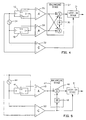
- Permanent magnet structure 11 is shown as having an E configuration, with gap 12 formed between middle leg segments 13 and 14.
- the magnet is comprised of magnet elements 11A and 11B and iron pole pieces 11C and 11D.
- Hall sensors 15 and 16 are mounted on surface 17, which is contemplated to be a flexible printed circuit board providing all the external connectibns required between the Hall sensors and circuitry to which they are connected by means of the leads in tail 18.
- Sample 21 is placed in a defined pattern (generally 1mm x 2mm) on substrate 22 and is moved into gap 12 past Hall sensors 15 and 16 to provide output signals from the Fig. 4 circuitry, for example, as discussed in detail below. Further details of this motion and the sensor outputs will be set out later in discussing Figs. 7 and 8.
- substrate 22 may be formed with extension 20 on which is printed bar code 19.
- the bar code is read by optical detector or bar code reader 28, shown with appropriate electrical leads 29.
- the bar code is spaced from sample pattern 21 by a predetermined distance and reader 28 has a fixed position with respect to the Hall sensors. The signals from the reader can then provide information about the position of the sample pattern with respect to the Hall sensors.
- the optical detector is a fairly sophisticated commercial device which issues two pulses each time one of the bar code lines passes through the detector.
- the first pulse corresponds to the leading edge of the bar coded line
- the second pulse in quadrature
- these pulses are used to trigger the data collection electronics which measures and stores the voltage output of the two Hall sensors, and these pulses are also used to control the current reversal when an AC current is used to bias the Hall sensors.
- the pulses from the optical detector (or perhaps a second optical detector) can be used to initiate and terminate the data collection process.
- the bar code information can tell the electronic control system when to start and stop the data collection, as well as provide the position information for each measurement of the signal from the Hall sensors as the sample moves past.
- Fig. 2 The principal of operation of a Hall sensor is shown in Fig. 2.
- Low frequency AC is applied at I+ and I- to bias or excite Hall sensor 15, the sensitive area 15B of which is on substrate 15A.
- Output voltages V+ and V- are applied to the Figs. 4 and 5 circuitry as will be explained in greater detail below.
- the applied magnetic field from magnet 11 is represented by arrow 23.
- the circuit of Fig. 4 relates to the Fig. 1 embodiment.
- This preferred embodiment has the Hall sensor pair excited by a low frequency alternating current 24.
- the output voltage signals from the sensor pair are sensed in a high impedance manner by amplifiers 25 and 26.
- This circuitry then produces signals indicative of the sum and difference of the sensor signals in the pair.
- Further signal processing by balancing stage 27 is accomplished by adjusting the balance gain by means of element 30 to minimize the output signal of this stage in the absence of a magnetic sample in the proximity of the sensors.
- the resultant signal from the balancing stage is then used as the signal input to lock-in stage 31.
- a reference input to the lock-in stage is preferably synchronously coupled from excitation source 24 via signal amplifier 32.
- the output of the lock-in stage represents the amount of particle material present. A suitable output could be obtained in other ways without the synchronously coupled excitation source to the lock-in stage.
- the lock-in stage is employed for signal processing by the lock-in technique.
- This technique is common and is also known as "phase sensitive detection,” “mixing,” and “heterodyning” in the art of signal processing. It is described as a signal processing stage having two inputs and an output.
- the technique entails exciting the measurement apparatus with an AC signal, and looking for an output signal synchronous to the alternating excitation. This technique serves to reject signal noise and interference present in the sensing apparatus.
- alternating excitation means 24 is the current used to excite the Hall sensors.
- a signal synchronous with the excitation signal is used as the "reference" input signal to the lock-in signal processing stage, as is commonly recognized in the art and as discussed above.
- the resultant difference signal from the sensors is configured as the other input to the lock-in stage.
- This difference signal may be optionally conditioned by the balancing stage mentioned above.
- the output signal of the lock-in stage will be indicative of the amount of particle material 21 present. It is desirable to select the excitation frequency such that signal detection occurs in a region of frequency space where sensor noise and interference are minimized. It may also be desirable to detect at a frequency that is a multiple of the excitation frequency.
- the actual implementation of the signal processing described above may in principle be accomplished by many available means, including active and passive analog electronics, digital signal processing, or a combination of these.
- the implementation may also include analog-to-digital or digital-to-analog conversion, or both.
- the requirement to pass the sample to be measured through a very narrow gap may not be acceptable in some applications.
- the requisite DC magnetic field may be generated by a configuration such as shown in Fig. 3, in which sharply shaped iron "pole tips" generate a DC magnetic field from the back side of the Hall sensors. While this so-called “single sided” magnet design does allow the use of larger and bulk substrates, it has the disadvantage that the_magnetic field at the position of the Hall sensors (and the sample) is non-uniform.
- the output of the Fig. 3 apparatus can be useful in situations where the Fig. 1 embodiment cannot be used and a good estimate of the particle count is needed.
- This measurement in the Fig. 3 apparatus is made by moving a well-defined pattern of magnetically susceptible particles 36 on substrate 37 into proximity of sensor 41 in the direction of arrow 42 and simultaneously in proximity to the magnetic field applied by means of permanent magnet structure 43.
- Magnet structure 43 is comprised of permanent magnet 38 and sharply shaped pole pieces 39, which are secured together by mounting device 40.
- the mounting device may be any non-conductive material such as plastic.
- the volume between pole pieces 39 and magnet 38 may be filed with plastic 40A. That may be a separate plastic element or it may be unitary with mounting device 40.
- Mounting device 40 is configured to be secured to a surface and holes 40B are provided to facilitate such attachment.
- the resulting signal as a function of distance between the patterned particles and the sensor, compared with the signal when no sample particles are present, is indicative of the amount of particle material 36.
- FIG. 5 A circuit diagram for the embodiment of Fig. 3 is shown in Fig. 5.
- Hall sensor 41 is excited by a low frequency alternating current 44.
- the output voltage signal from the sensor is sensed in a high impedance manner by amplifier 45.
- a signal proportional to the excitation is then summed at 46 with this signal indicative of the voltage across the sensor.
- Signal balancing occurs by adjusting the balancing gain in balancing stage 47 with balancing device 48 to minimize the output signal of this stage in the absence of a magnetic sample in the proximity of the sensors.
- the resulting sum signal is then detected by lock-in stage 51 using a reference signal synchronous to the excitation signal through amplifier 52 in the same manner as described in the preferred gradiometer embodiment above.
- the output of the lock-in stage represents the amount of particle material 36 present.
- the invention contemplates two ways to bias the Hall sensors.
- Hall sensors 15, 16 are connected in series, so exactly the same bias current flows in both sensors. Since any variations in the bias current cause a change in the output voltage, any changes in one sensor will be exactly cancelled by the exact same change (of the opposite sign) in the other sensor. However, since there is also a significant voltage drop along the length of each of the Hall sensors, this also means that the voltage points labeled V+ on the two Hall sensors are at rather different voltage potentials. This prevents simply connecting the V- connection at the first sensor to the V+ connection of the second sensor.
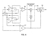
- FIG. 6 An alternative configuration is shown in Fig. 6 in which bias current 55 to the two Hall sensors 15, 16 is connected in parallel.
- This design is more susceptible to erroneous signals arising from variations in the bias current through one sensor, because such variations will not necessarily be exactly matched by a similar variation in the other sensor.
- the voltage potentials at the V+ and V- points on the two sensors will all be at about the same voltage. Indeed, if the sensors were perfectly matched, in the absence of any magnetic field (such that the Hall voltage is zero) all four of the voltage taps on the two sensors would be at exactly the same voltage.
- the voltage taps of the two Hall sensors are connected together and a single differential amplifier 56 is used to detect the difference of the Hall voltages across the two sensors.
- Reference input through amplifier 57 and balancing stage 58 and lock-in stage 59 function in the same manner as previously described.
- the parallel bias scheme might be preferred when using AC current bias, thereby eliminating the large voltage swings when using an AC bias with the sensors wired in series.
- the series bias scheme may be more desirable when using DC current bias.
- any combination of series/parallel and AC/DC can be used, depending on the features to be emphasized.
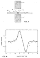
- Figs. 7 and 8 more details of the sensor response and relative motion of the sample and sensors are provided.
- the sensor signal (Fig. 8), recorded as a function of position, reflects the geometry of the sample pattern and the spatial response of the sensor. If there are two sensors in a gradiometer configuration, as in Fig. 1, the sample will generate a signal of one polarity while close to one sensor, it will generate a signal of the opposite polarity while close to the other sensor.
- Fig. 8 illustrates an ensemble of measurements plotted versus sample position.
- the solid curve represents a curve fit of an ideal response function using the method of least squares. It is clear that using both the position and signal voltage information, an absolute calculation of the magnetic moment of the sample can be derived. This is independent of the level of magnetic background and independent of any electronic or imbalance offsets in the signal voltage.
- the magnet pole pieces are preferably made of iron, the requirement is to have high magnetic permeability. They could be made of cobalt, nickel, or an appropriate alloy having the necessary characteristics.
- the pole pieces could be curved so that the gap, such as gap 12, is out front. Instead of the two magnets of Fig. 1, a single C-shaped magnet could be used.
- Substrate 22 could be a lateral flow membrane having region of interest 21.
- the substrate is preferably non-conductive and made of non-magnetic material, and could be made of plastic, wood, or other material satisfying these requirements.
- Substrate 22 can be moved by hand past the sensors, or the motion may be mechanized by using a stepper motor, a servo motor, or other means of generating motion by which the sample is moved relative to the sensors.
- the manner of motion is not critical to the invention.
- the system of the invention has excellent sensitivity, in the range of 1 nanovolt to 10 microvolts.
- the invention is for a very sensitive magnetic sensor in the presence of large fields (500-1000 Oersted) to detect very small signals.
- the signals detected are changes in the magnetic field due to the presence of the target particles and the changes may be in the order of milli-Oersteds.
Landscapes
- Physics & Mathematics (AREA)
- Chemical & Material Sciences (AREA)
- General Physics & Mathematics (AREA)
- Health & Medical Sciences (AREA)
- Chemical Kinetics & Catalysis (AREA)
- Electrochemistry (AREA)
- Condensed Matter Physics & Semiconductors (AREA)
- Life Sciences & Earth Sciences (AREA)
- Analytical Chemistry (AREA)
- Biochemistry (AREA)
- General Health & Medical Sciences (AREA)
- Immunology (AREA)
- Pathology (AREA)
- Investigating Or Analyzing Materials By The Use Of Magnetic Means (AREA)
- Measuring Magnetic Variables (AREA)
Applications Claiming Priority (3)
| Application Number | Priority Date | Filing Date | Title |
|---|---|---|---|
| US785403 | 2001-02-16 | ||
| US09/785,403 US6518747B2 (en) | 2001-02-16 | 2001-02-16 | Method and apparatus for quantitative determination of accumulations of magnetic particles |
| PCT/US2002/005116 WO2002067004A1 (en) | 2001-02-16 | 2002-02-12 | Method and apparatus for detection and measurement of accumulations of magnetic particles |
Publications (2)
| Publication Number | Publication Date |
|---|---|
| EP1360515A1 EP1360515A1 (en) | 2003-11-12 |
| EP1360515B1 true EP1360515B1 (en) | 2006-09-13 |
Family
ID=25135405
Family Applications (1)
| Application Number | Title | Priority Date | Filing Date |
|---|---|---|---|
| EP02719038A Expired - Lifetime EP1360515B1 (en) | 2001-02-16 | 2002-02-12 | Method and apparatus for detection and measurement of accumulations of magnetic particles |
Country Status (8)
| Country | Link |
|---|---|
| US (1) | US6518747B2 (enExample) |
| EP (1) | EP1360515B1 (enExample) |
| JP (1) | JP2004519666A (enExample) |
| CN (1) | CN1300598C (enExample) |
| AT (1) | ATE339696T1 (enExample) |
| CA (1) | CA2438423C (enExample) |
| DE (1) | DE60214674T2 (enExample) |
| WO (1) | WO2002067004A1 (enExample) |
Families Citing this family (129)
| Publication number | Priority date | Publication date | Assignee | Title |
|---|---|---|---|---|
| US6897654B2 (en) * | 2002-04-12 | 2005-05-24 | California Institute Of Technology | System and method of magnetic resonance imaging |
| US8697029B2 (en) * | 2002-04-18 | 2014-04-15 | The Regents Of The University Of Michigan | Modulated physical and chemical sensors |
| JP4066716B2 (ja) * | 2002-05-28 | 2008-03-26 | アイシン精機株式会社 | 位置検出センサ |
| EP1525447A4 (en) * | 2002-05-31 | 2006-12-06 | Univ California | METHOD AND DEVICE FOR DETECTING INTERESTING SUBSTANCES |
| WO2005111597A1 (ja) * | 2004-05-17 | 2005-11-24 | The Circle For The Promotion Of Science And Engineering | 磁性微粒子の検出装置 |
| US20090224755A1 (en) * | 2004-11-30 | 2009-09-10 | Koninklijke Philips Electronics, N.V. | Means and method for sensing a magnetic stray field in biosensors |
| EP1679524A1 (en) * | 2005-01-11 | 2006-07-12 | Ecole Polytechnique Federale De Lausanne Epfl - Sti - Imm - Lmis3 | Hall sensor and method of operating a Hall sensor |
| US7300631B2 (en) | 2005-05-02 | 2007-11-27 | Bioscale, Inc. | Method and apparatus for detection of analyte using a flexural plate wave device and magnetic particles |
| US7611908B2 (en) * | 2005-05-02 | 2009-11-03 | Bioscale, Inc. | Method and apparatus for therapeutic drug monitoring using an acoustic device |
| US7648844B2 (en) * | 2005-05-02 | 2010-01-19 | Bioscale, Inc. | Method and apparatus for detection of analyte using an acoustic device |
| US7749445B2 (en) * | 2005-05-02 | 2010-07-06 | Bioscale, Inc. | Method and apparatus for analyzing bioprocess fluids |
| GB0522968D0 (en) | 2005-11-11 | 2005-12-21 | Popovich Milan M | Holographic illumination device |
| JP4801447B2 (ja) * | 2006-01-13 | 2011-10-26 | 旭化成株式会社 | 磁気センサを用いた測定装置及び測定方法 |
| JP4676361B2 (ja) * | 2006-03-09 | 2011-04-27 | 株式会社日立製作所 | 磁気的免疫検査装置 |
| CN101400984A (zh) * | 2006-03-15 | 2009-04-01 | 皇家飞利浦电子股份有限公司 | 具有交变激励场的传感器设备 |
| US9329181B2 (en) * | 2006-03-21 | 2016-05-03 | Magnisense Technology Limited | Magnetic immunochromatographic test method and device |
| GB0718706D0 (en) | 2007-09-25 | 2007-11-07 | Creative Physics Ltd | Method and apparatus for reducing laser speckle |
| WO2007129262A1 (en) * | 2006-05-10 | 2007-11-15 | Koninklijke Philips Electronics N.V. | Magneto-resistive sensors with improved output signal characteristics |
| US8133439B2 (en) | 2006-08-01 | 2012-03-13 | Magic Technologies, Inc. | GMR biosensor with enhanced sensitivity |
| US7729093B1 (en) * | 2006-09-28 | 2010-06-01 | Headway Technologies, Inc. | Detection of magnetic beads using a magnetoresistive device together with ferromagnetic resonance |
| US8217647B2 (en) * | 2006-12-19 | 2012-07-10 | Koninklijke Philips Electronics N.V. | Measuring agglutination parameters |
| US8970215B2 (en) * | 2007-01-12 | 2015-03-03 | Koninklijkle Philips N.V. | Sensor device for and a method of sensing particles |
| US9068977B2 (en) * | 2007-03-09 | 2015-06-30 | The Regents Of The University Of Michigan | Non-linear rotation rates of remotely driven particles and uses thereof |
| US20100144939A1 (en) * | 2007-03-19 | 2010-06-10 | Koji Okada | Flame Retardant Polycarbonate Resin Composition |
| US8283912B2 (en) * | 2007-04-03 | 2012-10-09 | Koninklijke Philips Electronics N.V. | Sensor device with magnetic washing means |
| US9752615B2 (en) | 2007-06-27 | 2017-09-05 | Brooks Automation, Inc. | Reduced-complexity self-bearing brushless DC motor |
| US8823294B2 (en) * | 2007-06-27 | 2014-09-02 | Brooks Automation, Inc. | Commutation of an electromagnetic propulsion and guidance system |
| US8659205B2 (en) | 2007-06-27 | 2014-02-25 | Brooks Automation, Inc. | Motor stator with lift capability and reduced cogging characteristics |
| KR101660894B1 (ko) | 2007-06-27 | 2016-10-10 | 브룩스 오토메이션 인코퍼레이티드 | 다차원 위치 센서 |
| US8283813B2 (en) | 2007-06-27 | 2012-10-09 | Brooks Automation, Inc. | Robot drive with magnetic spindle bearings |
| JP5416104B2 (ja) * | 2007-06-27 | 2014-02-12 | ブルックス オートメーション インコーポレイテッド | セルフベアリングモータ用位置フィードバック |
| CN101754811A (zh) * | 2007-07-09 | 2010-06-23 | 皇家飞利浦电子股份有限公司 | 具有磁场发生器的微电子传感器设备以及载体 |
| CN101801817B (zh) | 2007-07-17 | 2015-07-22 | 布鲁克斯自动化公司 | 具备集成到室壁上的电动机的基片加工装置 |
| US8354280B2 (en) * | 2007-09-06 | 2013-01-15 | Bioscale, Inc. | Reusable detection surfaces and methods of using same |
| FR2922472B1 (fr) * | 2007-10-22 | 2010-04-02 | Snecma | Dispositif et procede de detection,de localisation et de comptage de billes de grenaillage dans une piece mecanique creuse |
| CN101281191B (zh) * | 2007-11-14 | 2012-10-10 | 石西增 | 一种对磁敏传感生物芯片进行自动测量的仪器 |
| US8154273B2 (en) * | 2008-10-10 | 2012-04-10 | Beckman Coulter, Inc. | Detecting and handling coincidence in particle analysis |
| EP2219033B1 (en) | 2008-12-30 | 2016-05-25 | MicroCoat Biotechnologie GmbH | Device, instrument and process for detecting magnetically labeled analytes |
| US9335604B2 (en) | 2013-12-11 | 2016-05-10 | Milan Momcilo Popovich | Holographic waveguide display |
| US11726332B2 (en) | 2009-04-27 | 2023-08-15 | Digilens Inc. | Diffractive projection apparatus |
| DE102010009161A1 (de) | 2010-02-24 | 2011-08-25 | Technische Hochschule Mittelhessen, 35390 | Verbesserung der Nachweisgrenze von magnetisch markierten Proben |
| JP5560334B2 (ja) * | 2010-07-21 | 2014-07-23 | 株式会社日立製作所 | 磁場計測装置 |
| WO2012027747A2 (en) | 2010-08-27 | 2012-03-01 | The Regents Of The University Of Michigan | Asynchronous magnetic bead rotation sensing systems and methods |
| WO2012136970A1 (en) | 2011-04-07 | 2012-10-11 | Milan Momcilo Popovich | Laser despeckler based on angular diversity |
| US9816993B2 (en) | 2011-04-11 | 2017-11-14 | The Regents Of The University Of Michigan | Magnetically induced microspinning for super-detection and super-characterization of biomarkers and live cells |
| DE102011017096A1 (de) * | 2011-04-14 | 2012-10-18 | Austriamicrosystems Ag | Hall-Sensor-Halbleiterbauelement und Verfahren zum Betrieb des Hall-Sensor-Halbleiterbauelementes |
| HUE034396T2 (en) | 2011-07-12 | 2018-02-28 | Foodchek Systems Inc | Culture media, Method for Salmonella and E. coli cultivation and Method for Detection of Salmonella and E. coli |
| WO2016020630A2 (en) | 2014-08-08 | 2016-02-11 | Milan Momcilo Popovich | Waveguide laser illuminator incorporating a despeckler |
| EP2995986B1 (en) | 2011-08-24 | 2017-04-12 | Rockwell Collins, Inc. | Data display |
| US10670876B2 (en) | 2011-08-24 | 2020-06-02 | Digilens Inc. | Waveguide laser illuminator incorporating a despeckler |
| ES2608930T3 (es) | 2012-01-04 | 2017-04-17 | Magnomics, S.A. | Dispositivo monolítico que combina CMOS con sensores magnetorresistivos |
| US20150010265A1 (en) | 2012-01-06 | 2015-01-08 | Milan, Momcilo POPOVICH | Contact image sensor using switchable bragg gratings |
| EP2842003B1 (en) | 2012-04-25 | 2019-02-27 | Rockwell Collins, Inc. | Holographic wide angle display |
| US9797817B2 (en) | 2012-05-03 | 2017-10-24 | The Regents Of The University Of Michigan | Multi-mode separation for target detection |
| US9456744B2 (en) | 2012-05-11 | 2016-10-04 | Digilens, Inc. | Apparatus for eye tracking |
| EP2685273A1 (en) * | 2012-07-13 | 2014-01-15 | Université Montpellier 2, Sciences et Techniques | Micromagnetometry detection system and method for detecting magnetic signatures of magnetic materials |
| US20140028305A1 (en) * | 2012-07-27 | 2014-01-30 | International Business Machines Corporation | Hall measurement system with rotary magnet |
| US9933684B2 (en) | 2012-11-16 | 2018-04-03 | Rockwell Collins, Inc. | Transparent waveguide display providing upper and lower fields of view having a specific light output aperture configuration |
| US10209517B2 (en) | 2013-05-20 | 2019-02-19 | Digilens, Inc. | Holographic waveguide eye tracker |
| US9727772B2 (en) | 2013-07-31 | 2017-08-08 | Digilens, Inc. | Method and apparatus for contact image sensing |
| US9360294B2 (en) * | 2013-10-31 | 2016-06-07 | Ascension Technology Corporation | Magnetic sensors |
| US9983110B2 (en) | 2013-11-04 | 2018-05-29 | The Regents Of The University Of Michigan | Asynchronous magnetic bead rotation (AMBR) microviscometer for analysis of analytes |
| KR102686315B1 (ko) | 2013-11-13 | 2024-07-19 | 브룩스 오토메이션 인코퍼레이티드 | 씰링된 로봇 드라이브 |
| US10348172B2 (en) | 2013-11-13 | 2019-07-09 | Brooks Automation, Inc. | Sealed switched reluctance motor |
| KR20220000416A (ko) | 2013-11-13 | 2022-01-03 | 브룩스 오토메이션 인코퍼레이티드 | 브러쉬리스 전기 기계 제어 방법 및 장치 |
| TWI695447B (zh) | 2013-11-13 | 2020-06-01 | 布魯克斯自動機械公司 | 運送設備 |
| US9910105B2 (en) | 2014-03-20 | 2018-03-06 | Lockheed Martin Corporation | DNV magnetic field detector |
| US9557391B2 (en) | 2015-01-23 | 2017-01-31 | Lockheed Martin Corporation | Apparatus and method for high sensitivity magnetometry measurement and signal processing in a magnetic detection system |
| US9614589B1 (en) | 2015-12-01 | 2017-04-04 | Lockheed Martin Corporation | Communication via a magnio |
| US10338162B2 (en) | 2016-01-21 | 2019-07-02 | Lockheed Martin Corporation | AC vector magnetic anomaly detection with diamond nitrogen vacancies |
| US9274041B2 (en) * | 2014-04-15 | 2016-03-01 | Spectro Scientific, Inc. | Particle counter and classification system |
| WO2016020632A1 (en) | 2014-08-08 | 2016-02-11 | Milan Momcilo Popovich | Method for holographic mastering and replication |
| US10241330B2 (en) | 2014-09-19 | 2019-03-26 | Digilens, Inc. | Method and apparatus for generating input images for holographic waveguide displays |
| US10423222B2 (en) | 2014-09-26 | 2019-09-24 | Digilens Inc. | Holographic waveguide optical tracker |
| CN104502242A (zh) * | 2014-11-20 | 2015-04-08 | 北京航空航天大学 | 一种基于径向磁场的双边对称结构在线磨粒监测方法及监测传感器 |
| US20180275402A1 (en) | 2015-01-12 | 2018-09-27 | Digilens, Inc. | Holographic waveguide light field displays |
| WO2016113534A1 (en) | 2015-01-12 | 2016-07-21 | Milan Momcilo Popovich | Environmentally isolated waveguide display |
| JP6867947B2 (ja) | 2015-01-20 | 2021-05-12 | ディジレンズ インコーポレイテッド | ホログラフィック導波路ライダー |
| WO2016126436A1 (en) | 2015-02-04 | 2016-08-11 | Lockheed Martin Corporation | Apparatus and method for recovery of three dimensional magnetic field from a magnetic detection system |
| US9632226B2 (en) | 2015-02-12 | 2017-04-25 | Digilens Inc. | Waveguide grating device |
| WO2016146963A1 (en) | 2015-03-16 | 2016-09-22 | Popovich, Milan, Momcilo | Waveguide device incorporating a light pipe |
| US10591756B2 (en) | 2015-03-31 | 2020-03-17 | Digilens Inc. | Method and apparatus for contact image sensing |
| US9678040B2 (en) | 2015-04-09 | 2017-06-13 | International Business Machines Corporation | Rotating magnetic field hall measurement system |
| EP3359999A1 (en) | 2015-10-05 | 2018-08-15 | Popovich, Milan Momcilo | Waveguide display |
| WO2017127096A1 (en) | 2016-01-21 | 2017-07-27 | Lockheed Martin Corporation | Diamond nitrogen vacancy sensor with dual rf sources |
| CN109073889B (zh) | 2016-02-04 | 2021-04-27 | 迪吉伦斯公司 | 全息波导光学跟踪器 |
| EP3208627B1 (en) * | 2016-02-19 | 2021-09-01 | Université de Montpellier | Measurement system and method for characterizing at least one single magnetic object |
| EP3433659B1 (en) | 2016-03-24 | 2024-10-23 | DigiLens, Inc. | Method and apparatus for providing a polarization selective holographic waveguide device |
| US10890707B2 (en) | 2016-04-11 | 2021-01-12 | Digilens Inc. | Holographic waveguide apparatus for structured light projection |
| US10345396B2 (en) | 2016-05-31 | 2019-07-09 | Lockheed Martin Corporation | Selected volume continuous illumination magnetometer |
| US10338163B2 (en) | 2016-07-11 | 2019-07-02 | Lockheed Martin Corporation | Multi-frequency excitation schemes for high sensitivity magnetometry measurement with drift error compensation |
| US10371765B2 (en) | 2016-07-11 | 2019-08-06 | Lockheed Martin Corporation | Geolocation of magnetic sources using vector magnetometer sensors |
| US10527746B2 (en) | 2016-05-31 | 2020-01-07 | Lockheed Martin Corporation | Array of UAVS with magnetometers |
| US10359479B2 (en) | 2017-02-20 | 2019-07-23 | Lockheed Martin Corporation | Efficient thermal drift compensation in DNV vector magnetometry |
| US10330744B2 (en) | 2017-03-24 | 2019-06-25 | Lockheed Martin Corporation | Magnetometer with a waveguide |
| US10408890B2 (en) | 2017-03-24 | 2019-09-10 | Lockheed Martin Corporation | Pulsed RF methods for optimization of CW measurements |
| US10571530B2 (en) | 2016-05-31 | 2020-02-25 | Lockheed Martin Corporation | Buoy array of magnetometers |
| US10677953B2 (en) | 2016-05-31 | 2020-06-09 | Lockheed Martin Corporation | Magneto-optical detecting apparatus and methods |
| US10317279B2 (en) | 2016-05-31 | 2019-06-11 | Lockheed Martin Corporation | Optical filtration system for diamond material with nitrogen vacancy centers |
| US10345395B2 (en) | 2016-12-12 | 2019-07-09 | Lockheed Martin Corporation | Vector magnetometry localization of subsurface liquids |
| US11513350B2 (en) | 2016-12-02 | 2022-11-29 | Digilens Inc. | Waveguide device with uniform output illumination |
| WO2018129398A1 (en) | 2017-01-05 | 2018-07-12 | Digilens, Inc. | Wearable heads up displays |
| GB2558905A (en) * | 2017-01-19 | 2018-07-25 | Mids Medical Ltd | Device and method for accurate measurement of magnetic particles in assay apparatus |
| US10371760B2 (en) | 2017-03-24 | 2019-08-06 | Lockheed Martin Corporation | Standing-wave radio frequency exciter |
| US10459041B2 (en) | 2017-03-24 | 2019-10-29 | Lockheed Martin Corporation | Magnetic detection system with highly integrated diamond nitrogen vacancy sensor |
| US10338164B2 (en) | 2017-03-24 | 2019-07-02 | Lockheed Martin Corporation | Vacancy center material with highly efficient RF excitation |
| US20180275207A1 (en) * | 2017-03-24 | 2018-09-27 | Lockheed Martin Corporation | Magneto-optical defect center sensor with vivaldi rf antenna array |
| US10379174B2 (en) | 2017-03-24 | 2019-08-13 | Lockheed Martin Corporation | Bias magnet array for magnetometer |
| JP7399084B2 (ja) | 2017-10-16 | 2023-12-15 | ディジレンズ インコーポレイテッド | ピクセル化されたディスプレイの画像分解能を倍増させるためのシステムおよび方法 |
| WO2019136476A1 (en) | 2018-01-08 | 2019-07-11 | Digilens, Inc. | Waveguide architectures and related methods of manufacturing |
| WO2019136473A1 (en) | 2018-01-08 | 2019-07-11 | Digilens, Inc. | Methods for fabricating optical waveguides |
| KR102768598B1 (ko) | 2018-01-08 | 2025-02-13 | 디지렌즈 인코포레이티드. | 도파관 셀 내의 홀로그래픽 격자의 높은 처리능력의 레코딩을 위한 시스템 및 방법 |
| KR102819207B1 (ko) | 2018-01-08 | 2025-06-11 | 디지렌즈 인코포레이티드. | 도파관 셀을 제조하기 위한 시스템 및 방법 |
| JP7487109B2 (ja) | 2018-03-16 | 2024-05-20 | ディジレンズ インコーポレイテッド | 複屈折制御を組み込むホログラフィック導波管およびその加工のための方法 |
| WO2020023779A1 (en) | 2018-07-25 | 2020-01-30 | Digilens Inc. | Systems and methods for fabricating a multilayer optical structure |
| DE102018008519A1 (de) * | 2018-10-30 | 2020-04-30 | Giesecke+Devrient Currency Technology Gmbh | Magnetische Prüfung von Wertdokumenten |
| WO2020149956A1 (en) | 2019-01-14 | 2020-07-23 | Digilens Inc. | Holographic waveguide display with light control layer |
| WO2020163524A1 (en) | 2019-02-05 | 2020-08-13 | Digilens Inc. | Methods for compensating for optical surface nonuniformity |
| EP3924759B1 (en) | 2019-02-15 | 2025-07-30 | Digilens Inc. | Methods and apparatuses for providing a holographic waveguide display using integrated gratings |
| US20220283377A1 (en) | 2019-02-15 | 2022-09-08 | Digilens Inc. | Wide Angle Waveguide Display |
| US20200292745A1 (en) | 2019-03-12 | 2020-09-17 | Digilens Inc. | Holographic Waveguide Backlight and Related Methods of Manufacturing |
| CN114207492A (zh) | 2019-06-07 | 2022-03-18 | 迪吉伦斯公司 | 带透射光栅和反射光栅的波导及其生产方法 |
| CN114341729A (zh) | 2019-07-29 | 2022-04-12 | 迪吉伦斯公司 | 用于使像素化显示器的图像分辨率和视场倍增的方法和设备 |
| KR102775783B1 (ko) | 2019-08-29 | 2025-02-28 | 디지렌즈 인코포레이티드. | 진공 격자 및 이의 제조 방법 |
| WO2022140763A1 (en) | 2020-12-21 | 2022-06-30 | Digilens Inc. | Eye glow suppression in waveguide based displays |
| WO2022150841A1 (en) | 2021-01-07 | 2022-07-14 | Digilens Inc. | Grating structures for color waveguides |
| JP2024508926A (ja) | 2021-03-05 | 2024-02-28 | ディジレンズ インコーポレイテッド | 真空周期的構造体および製造の方法 |
| ES2927494B2 (es) * | 2021-12-22 | 2023-07-20 | Univ Madrid Politecnica | Aparato para medir la susceptibilidad magnética de muestras minerales |
| CN114779351A (zh) * | 2022-05-10 | 2022-07-22 | 包头市英思特稀磁新材料股份有限公司 | 磁组件成品检验治具及磁组件成品生产线 |
Family Cites Families (26)
| Publication number | Priority date | Publication date | Assignee | Title |
|---|---|---|---|---|
| US3195043A (en) * | 1961-05-19 | 1965-07-13 | Westinghouse Electric Corp | Hall effect proximity transducer |
| DE1498531C3 (de) * | 1963-11-27 | 1973-11-29 | Varian Mat Gmbh, 2800 Bremen | Vorrichtung zur Bestimmung der Massenzahl aus der im Spalt des Trenn magneten eines Massenspektrometers herrschenden Feldstarke |
| US4037150A (en) * | 1973-05-30 | 1977-07-19 | Sergei Glebovich Taranov | Method of and apparatus for eliminating the effect of non-equipotentiality voltage on the hall voltage |
| US4518919A (en) * | 1981-01-16 | 1985-05-21 | Tokyo Shibaura Denki Kabushiki Kaisha | Detecting device for detecting a magnetic strip embedded in a sheet |
| AT373174B (de) * | 1982-06-23 | 1983-12-27 | Voest Alpine Ag | Vorrichtung zum zufuehren von blechtafeln zu einer biegemaschine |
| US4537861A (en) | 1983-02-03 | 1985-08-27 | Elings Virgil B | Apparatus and method for homogeneous immunoassay |
| GB8408529D0 (en) | 1984-04-03 | 1984-05-16 | Health Lab Service Board | Concentration of biological particles |
| EP0167196B1 (de) * | 1984-07-05 | 1988-09-07 | De La Rue Giori S.A. | Verfahren zum Verarbeiten von Wertscheinbahnen oder Wertscheinbogen zu Wertscheinbündeln |
| JPS6390765A (ja) | 1986-10-03 | 1988-04-21 | Nippon Telegr & Teleph Corp <Ntt> | Squid免疫測定法 |
| GB8717201D0 (en) | 1987-07-21 | 1987-08-26 | Manchester Lasers Ltd | Magnetic sensor |
| JPH0619469B2 (ja) | 1988-04-13 | 1994-03-16 | 大和製衡株式会社 | 金属等の異物混入検出器 |
| US4913863A (en) | 1989-01-30 | 1990-04-03 | Hoechst Celanese Corporation | Split extrusion die assembly for thermoplastic materials and methods of using the same |
| US5001424A (en) | 1989-02-03 | 1991-03-19 | Product Resources, Inc. | Apparatus for measuring magnetic particles suspended in a fluid based on fluctuations in an induced voltage |
| TW199858B (enExample) | 1990-03-30 | 1993-02-11 | Fujirebio Kk | |
| DE4022739A1 (de) * | 1990-07-17 | 1992-01-23 | Gao Ges Automation Org | Vorrichtung zur pruefung von mit magnetischen eigenschaften ausgestatteten messobjekten |
| IL100866A (en) * | 1991-02-06 | 1995-10-31 | Igen Inc | Method and apparatus for magnetic microparticulate based luminescence assay including plurality of magnets |
| FR2679660B1 (fr) | 1991-07-22 | 1993-11-12 | Pasteur Diagnostics | Procede et dispositif magnetique d'analyse immunologique sur phase solide. |
| US5445970A (en) | 1992-03-20 | 1995-08-29 | Abbott Laboratories | Magnetically assisted binding assays using magnetically labeled binding members |
| US5445971A (en) | 1992-03-20 | 1995-08-29 | Abbott Laboratories | Magnetically assisted binding assays using magnetically labeled binding members |
| AU686604B2 (en) | 1993-05-17 | 1998-02-12 | Fujirebio Inc. | Method and apparatus for performing an indirect agglutination immunoassay |
| US5486457A (en) | 1993-08-25 | 1996-01-23 | Children's Medical Center Corporation | Method and system for measurement of mechanical properties of molecules and cells |
| JPH07210833A (ja) * | 1994-01-11 | 1995-08-11 | Murata Mfg Co Ltd | 磁気センサ装置 |
| US5656429A (en) | 1994-10-03 | 1997-08-12 | Adelman; Lonnie W. | Polynucleotide and protein analysis method using magnetizable moieties |
| CN2207510Y (zh) * | 1994-11-11 | 1995-09-13 | 钱淑俊 | 多功能探照灯装置 |
| US6046585A (en) | 1997-11-21 | 2000-04-04 | Quantum Design, Inc. | Method and apparatus for making quantitative measurements of localized accumulations of target particles having magnetic particles bound thereto |
| JP4024964B2 (ja) * | 1998-07-28 | 2007-12-19 | キヤノン電子株式会社 | 磁気インク検知用磁気センサー、その信号処理方法、及び磁気インク検知装置 |
-
2001
- 2001-02-16 US US09/785,403 patent/US6518747B2/en not_active Expired - Lifetime
-
2002
- 2002-02-12 CN CNB028003187A patent/CN1300598C/zh not_active Expired - Fee Related
- 2002-02-12 AT AT02719038T patent/ATE339696T1/de not_active IP Right Cessation
- 2002-02-12 JP JP2002566677A patent/JP2004519666A/ja active Pending
- 2002-02-12 DE DE60214674T patent/DE60214674T2/de not_active Expired - Lifetime
- 2002-02-12 EP EP02719038A patent/EP1360515B1/en not_active Expired - Lifetime
- 2002-02-12 WO PCT/US2002/005116 patent/WO2002067004A1/en not_active Ceased
- 2002-02-12 CA CA002438423A patent/CA2438423C/en not_active Expired - Fee Related
Also Published As
| Publication number | Publication date |
|---|---|
| DE60214674D1 (de) | 2006-10-26 |
| CN1300598C (zh) | 2007-02-14 |
| WO2002067004A1 (en) | 2002-08-29 |
| US20020135358A1 (en) | 2002-09-26 |
| US6518747B2 (en) | 2003-02-11 |
| HK1058550A1 (en) | 2004-05-21 |
| CA2438423A1 (en) | 2002-08-29 |
| ATE339696T1 (de) | 2006-10-15 |
| EP1360515A1 (en) | 2003-11-12 |
| WO2002067004B1 (en) | 2002-10-24 |
| CA2438423C (en) | 2009-09-15 |
| DE60214674T2 (de) | 2007-09-13 |
| CN1457434A (zh) | 2003-11-19 |
| JP2004519666A (ja) | 2004-07-02 |
Similar Documents
| Publication | Publication Date | Title |
|---|---|---|
| EP1360515B1 (en) | Method and apparatus for detection and measurement of accumulations of magnetic particles | |
| EP1036328B1 (en) | Method and apparatus for making quantitave measurements of localized accumulations of magnetic particles | |
| Baselt et al. | Biosensor based on force microscope technology | |
| US6597176B2 (en) | Method and apparatus for making measurements of patterns of magnetic particles in lateral flow membranes and microfluidic systems | |
| US20090224755A1 (en) | Means and method for sensing a magnetic stray field in biosensors | |
| US20090072815A1 (en) | Calibration of a magnetic sensor device | |
| CN101454683A (zh) | 具有自适应场补偿的传感器设备 | |
| WO2005010542A2 (en) | On-chip magnetic particle sensor with improved snr | |
| WO2005010543A1 (en) | On-chip magnetic sensor device with suppressed cross-talk | |
| US20130121879A1 (en) | Magnetic-Field Measurement Device | |
| CN101315429B (zh) | 目标物质检测套件和目标物质检测方法 | |
| CN101438180A (zh) | 具有改进的输出信号特性的磁电阻传感器 | |
| KR101235845B1 (ko) | 자기저항센서를 이용한 검출시스템 및 이를 이용한 검출방법 | |
| HK1058550B (en) | Method and apparatus for detection and measurement of accumulations of magnetic particles | |
| KR20120087668A (ko) | 자기저항센서를 이용한 검출시스템 및 이를 이용한 검출방법 |
Legal Events
| Date | Code | Title | Description |
|---|---|---|---|
| PUAI | Public reference made under article 153(3) epc to a published international application that has entered the european phase |
Free format text: ORIGINAL CODE: 0009012 |
|
| 17P | Request for examination filed |
Effective date: 20030717 |
|
| AK | Designated contracting states |
Kind code of ref document: A1 Designated state(s): AT BE CH CY DE DK ES FI FR GB GR IE IT LI LU MC NL PT SE TR |
|
| AX | Request for extension of the european patent |
Extension state: AL LT LV MK RO SI |
|
| RIN1 | Information on inventor provided before grant (corrected) |
Inventor name: BLACK, RANDALL, C. Inventor name: SIMMONDS, MICHAEL, B. Inventor name: DIEDERICHS, JOST, H. Inventor name: JENSEN, KURT, G. Inventor name: SAGER, RONALD, E. |
|
| 17Q | First examination report despatched |
Effective date: 20041126 |
|
| GRAP | Despatch of communication of intention to grant a patent |
Free format text: ORIGINAL CODE: EPIDOSNIGR1 |
|
| GRAS | Grant fee paid |
Free format text: ORIGINAL CODE: EPIDOSNIGR3 |
|
| GRAA | (expected) grant |
Free format text: ORIGINAL CODE: 0009210 |
|
| RAP1 | Party data changed (applicant data changed or rights of an application transferred) |
Owner name: QUANTUM DESIGN, INC. |
|
| AK | Designated contracting states |
Kind code of ref document: B1 Designated state(s): AT BE CH CY DE DK ES FI FR GB GR IE IT LI LU MC NL PT SE TR |
|
| PG25 | Lapsed in a contracting state [announced via postgrant information from national office to epo] |
Ref country code: CH Free format text: LAPSE BECAUSE OF FAILURE TO SUBMIT A TRANSLATION OF THE DESCRIPTION OR TO PAY THE FEE WITHIN THE PRESCRIBED TIME-LIMIT Effective date: 20060913 Ref country code: BE Free format text: LAPSE BECAUSE OF FAILURE TO SUBMIT A TRANSLATION OF THE DESCRIPTION OR TO PAY THE FEE WITHIN THE PRESCRIBED TIME-LIMIT Effective date: 20060913 Ref country code: IT Free format text: LAPSE BECAUSE OF FAILURE TO SUBMIT A TRANSLATION OF THE DESCRIPTION OR TO PAY THE FEE WITHIN THE PRESCRIBED TIME-LIMIT;WARNING: LAPSES OF ITALIAN PATENTS WITH EFFECTIVE DATE BEFORE 2007 MAY HAVE OCCURRED AT ANY TIME BEFORE 2007. THE CORRECT EFFECTIVE DATE MAY BE DIFFERENT FROM THE ONE RECORDED. Effective date: 20060913 Ref country code: LI Free format text: LAPSE BECAUSE OF FAILURE TO SUBMIT A TRANSLATION OF THE DESCRIPTION OR TO PAY THE FEE WITHIN THE PRESCRIBED TIME-LIMIT Effective date: 20060913 Ref country code: FI Free format text: LAPSE BECAUSE OF FAILURE TO SUBMIT A TRANSLATION OF THE DESCRIPTION OR TO PAY THE FEE WITHIN THE PRESCRIBED TIME-LIMIT Effective date: 20060913 Ref country code: AT Free format text: LAPSE BECAUSE OF FAILURE TO SUBMIT A TRANSLATION OF THE DESCRIPTION OR TO PAY THE FEE WITHIN THE PRESCRIBED TIME-LIMIT Effective date: 20060913 Ref country code: NL Free format text: LAPSE BECAUSE OF FAILURE TO SUBMIT A TRANSLATION OF THE DESCRIPTION OR TO PAY THE FEE WITHIN THE PRESCRIBED TIME-LIMIT Effective date: 20060913 |
|
| REG | Reference to a national code |
Ref country code: GB Ref legal event code: FG4D |
|
| REG | Reference to a national code |
Ref country code: CH Ref legal event code: EP |
|
| REG | Reference to a national code |
Ref country code: IE Ref legal event code: FG4D |
|
| REF | Corresponds to: |
Ref document number: 60214674 Country of ref document: DE Date of ref document: 20061026 Kind code of ref document: P |
|
| PG25 | Lapsed in a contracting state [announced via postgrant information from national office to epo] |
Ref country code: DK Free format text: LAPSE BECAUSE OF FAILURE TO SUBMIT A TRANSLATION OF THE DESCRIPTION OR TO PAY THE FEE WITHIN THE PRESCRIBED TIME-LIMIT Effective date: 20061213 Ref country code: SE Free format text: LAPSE BECAUSE OF FAILURE TO SUBMIT A TRANSLATION OF THE DESCRIPTION OR TO PAY THE FEE WITHIN THE PRESCRIBED TIME-LIMIT Effective date: 20061213 |
|
| PG25 | Lapsed in a contracting state [announced via postgrant information from national office to epo] |
Ref country code: ES Free format text: LAPSE BECAUSE OF FAILURE TO SUBMIT A TRANSLATION OF THE DESCRIPTION OR TO PAY THE FEE WITHIN THE PRESCRIBED TIME-LIMIT Effective date: 20061224 |
|
| PG25 | Lapsed in a contracting state [announced via postgrant information from national office to epo] |
Ref country code: PT Free format text: LAPSE BECAUSE OF FAILURE TO SUBMIT A TRANSLATION OF THE DESCRIPTION OR TO PAY THE FEE WITHIN THE PRESCRIBED TIME-LIMIT Effective date: 20070226 |
|
| PG25 | Lapsed in a contracting state [announced via postgrant information from national office to epo] |
Ref country code: MC Free format text: LAPSE BECAUSE OF NON-PAYMENT OF DUE FEES Effective date: 20070228 |
|
| NLV1 | Nl: lapsed or annulled due to failure to fulfill the requirements of art. 29p and 29m of the patents act | ||
| REG | Reference to a national code |
Ref country code: CH Ref legal event code: PL |
|
| ET | Fr: translation filed | ||
| PLBE | No opposition filed within time limit |
Free format text: ORIGINAL CODE: 0009261 |
|
| STAA | Information on the status of an ep patent application or granted ep patent |
Free format text: STATUS: NO OPPOSITION FILED WITHIN TIME LIMIT |
|
| 26N | No opposition filed |
Effective date: 20070614 |
|
| PG25 | Lapsed in a contracting state [announced via postgrant information from national office to epo] |
Ref country code: IE Free format text: LAPSE BECAUSE OF NON-PAYMENT OF DUE FEES Effective date: 20070212 |
|
| PG25 | Lapsed in a contracting state [announced via postgrant information from national office to epo] |
Ref country code: GR Free format text: LAPSE BECAUSE OF FAILURE TO SUBMIT A TRANSLATION OF THE DESCRIPTION OR TO PAY THE FEE WITHIN THE PRESCRIBED TIME-LIMIT Effective date: 20061214 |
|
| PG25 | Lapsed in a contracting state [announced via postgrant information from national office to epo] |
Ref country code: CY Free format text: LAPSE BECAUSE OF FAILURE TO SUBMIT A TRANSLATION OF THE DESCRIPTION OR TO PAY THE FEE WITHIN THE PRESCRIBED TIME-LIMIT Effective date: 20060913 Ref country code: LU Free format text: LAPSE BECAUSE OF NON-PAYMENT OF DUE FEES Effective date: 20070212 |
|
| PG25 | Lapsed in a contracting state [announced via postgrant information from national office to epo] |
Ref country code: TR Free format text: LAPSE BECAUSE OF FAILURE TO SUBMIT A TRANSLATION OF THE DESCRIPTION OR TO PAY THE FEE WITHIN THE PRESCRIBED TIME-LIMIT Effective date: 20060913 |
|
| REG | Reference to a national code |
Ref country code: FR Ref legal event code: PLFP Year of fee payment: 14 |
|
| PGFP | Annual fee paid to national office [announced via postgrant information from national office to epo] |
Ref country code: DE Payment date: 20150226 Year of fee payment: 14 |
|
| PGFP | Annual fee paid to national office [announced via postgrant information from national office to epo] |
Ref country code: FR Payment date: 20150217 Year of fee payment: 14 Ref country code: GB Payment date: 20150226 Year of fee payment: 14 |
|
| REG | Reference to a national code |
Ref country code: DE Ref legal event code: R119 Ref document number: 60214674 Country of ref document: DE |
|
| GBPC | Gb: european patent ceased through non-payment of renewal fee |
Effective date: 20160212 |
|
| REG | Reference to a national code |
Ref country code: FR Ref legal event code: ST Effective date: 20161028 |
|
| PG25 | Lapsed in a contracting state [announced via postgrant information from national office to epo] |
Ref country code: GB Free format text: LAPSE BECAUSE OF NON-PAYMENT OF DUE FEES Effective date: 20160212 Ref country code: DE Free format text: LAPSE BECAUSE OF NON-PAYMENT OF DUE FEES Effective date: 20160901 Ref country code: FR Free format text: LAPSE BECAUSE OF NON-PAYMENT OF DUE FEES Effective date: 20160229 |