EP1360034B1 - Article a abrasif fixe destine a la modification d'une tranche semi-conductrice - Google Patents
Article a abrasif fixe destine a la modification d'une tranche semi-conductrice Download PDFInfo
- Publication number
- EP1360034B1 EP1360034B1 EP01948459A EP01948459A EP1360034B1 EP 1360034 B1 EP1360034 B1 EP 1360034B1 EP 01948459 A EP01948459 A EP 01948459A EP 01948459 A EP01948459 A EP 01948459A EP 1360034 B1 EP1360034 B1 EP 1360034B1
- Authority
- EP
- European Patent Office
- Prior art keywords
- article
- rigid
- web
- abrasive
- rigid segments
- Prior art date
- Legal status (The legal status is an assumption and is not a legal conclusion. Google has not performed a legal analysis and makes no representation as to the accuracy of the status listed.)
- Expired - Lifetime
Links
- 239000004065 semiconductor Substances 0.000 title claims description 53
- 230000000051 modifying effect Effects 0.000 title claims description 16
- 239000002245 particle Substances 0.000 claims abstract description 19
- 239000000463 material Substances 0.000 claims description 33
- 238000000034 method Methods 0.000 claims description 33
- 239000002131 composite material Substances 0.000 claims description 17
- 239000000758 substrate Substances 0.000 claims description 11
- 239000002184 metal Substances 0.000 claims description 7
- 229910052751 metal Inorganic materials 0.000 claims description 7
- 229920003023 plastic Polymers 0.000 claims description 5
- 239000004033 plastic Substances 0.000 claims description 5
- 235000012431 wafers Nutrition 0.000 description 62
- 230000008569 process Effects 0.000 description 21
- 238000005498 polishing Methods 0.000 description 15
- 239000012858 resilient material Substances 0.000 description 11
- 239000000853 adhesive Substances 0.000 description 8
- 230000001070 adhesive effect Effects 0.000 description 8
- -1 polyperfluoroolefins Polymers 0.000 description 8
- 230000007717 exclusion Effects 0.000 description 7
- 239000006260 foam Substances 0.000 description 7
- 229920000620 organic polymer Polymers 0.000 description 7
- 239000011230 binding agent Substances 0.000 description 6
- 238000010276 construction Methods 0.000 description 6
- 229920001577 copolymer Polymers 0.000 description 6
- 239000000203 mixture Substances 0.000 description 6
- 239000002002 slurry Substances 0.000 description 6
- 239000000835 fiber Substances 0.000 description 5
- 230000007246 mechanism Effects 0.000 description 5
- 230000004048 modification Effects 0.000 description 5
- 238000012986 modification Methods 0.000 description 5
- VYPSYNLAJGMNEJ-UHFFFAOYSA-N Silicium dioxide Chemical compound O=[Si]=O VYPSYNLAJGMNEJ-UHFFFAOYSA-N 0.000 description 4
- 238000004519 manufacturing process Methods 0.000 description 4
- 229920000728 polyester Polymers 0.000 description 4
- 229920000098 polyolefin Polymers 0.000 description 4
- 238000012360 testing method Methods 0.000 description 4
- 239000004593 Epoxy Substances 0.000 description 3
- 239000004952 Polyamide Substances 0.000 description 3
- 239000004820 Pressure-sensitive adhesive Substances 0.000 description 3
- 230000006835 compression Effects 0.000 description 3
- 238000007906 compression Methods 0.000 description 3
- 238000007517 polishing process Methods 0.000 description 3
- 229920002647 polyamide Polymers 0.000 description 3
- 229920000642 polymer Polymers 0.000 description 3
- 229920002635 polyurethane Polymers 0.000 description 3
- 239000004814 polyurethane Substances 0.000 description 3
- 238000007655 standard test method Methods 0.000 description 3
- 239000000126 substance Substances 0.000 description 3
- 229920002725 thermoplastic elastomer Polymers 0.000 description 3
- 229920001187 thermosetting polymer Polymers 0.000 description 3
- VTYYLEPIZMXCLO-UHFFFAOYSA-L Calcium carbonate Chemical compound [Ca+2].[O-]C([O-])=O VTYYLEPIZMXCLO-UHFFFAOYSA-L 0.000 description 2
- 239000004831 Hot glue Substances 0.000 description 2
- RRHGJUQNOFWUDK-UHFFFAOYSA-N Isoprene Chemical compound CC(=C)C=C RRHGJUQNOFWUDK-UHFFFAOYSA-N 0.000 description 2
- 239000004698 Polyethylene Substances 0.000 description 2
- PPBRXRYQALVLMV-UHFFFAOYSA-N Styrene Chemical compound C=CC1=CC=CC=C1 PPBRXRYQALVLMV-UHFFFAOYSA-N 0.000 description 2
- 229910052782 aluminium Inorganic materials 0.000 description 2
- XAGFODPZIPBFFR-UHFFFAOYSA-N aluminium Chemical compound [Al] XAGFODPZIPBFFR-UHFFFAOYSA-N 0.000 description 2
- 229920001400 block copolymer Polymers 0.000 description 2
- 230000000694 effects Effects 0.000 description 2
- 125000003700 epoxy group Chemical group 0.000 description 2
- 239000005038 ethylene vinyl acetate Substances 0.000 description 2
- 239000007788 liquid Substances 0.000 description 2
- 150000002739 metals Chemical class 0.000 description 2
- 229920003052 natural elastomer Polymers 0.000 description 2
- 229920001194 natural rubber Polymers 0.000 description 2
- 229920001084 poly(chloroprene) Polymers 0.000 description 2
- 229920001200 poly(ethylene-vinyl acetate) Polymers 0.000 description 2
- 229920000515 polycarbonate Polymers 0.000 description 2
- 239000004417 polycarbonate Substances 0.000 description 2
- 229920000647 polyepoxide Polymers 0.000 description 2
- 229920000573 polyethylene Polymers 0.000 description 2
- 229920000915 polyvinyl chloride Polymers 0.000 description 2
- 239000011148 porous material Substances 0.000 description 2
- 230000002787 reinforcement Effects 0.000 description 2
- 229910001220 stainless steel Inorganic materials 0.000 description 2
- 239000010935 stainless steel Substances 0.000 description 2
- 229920001169 thermoplastic Polymers 0.000 description 2
- 239000004416 thermosoftening plastic Substances 0.000 description 2
- 238000012876 topography Methods 0.000 description 2
- 230000032258 transport Effects 0.000 description 2
- RYGMFSIKBFXOCR-UHFFFAOYSA-N Copper Chemical compound [Cu] RYGMFSIKBFXOCR-UHFFFAOYSA-N 0.000 description 1
- 229920002943 EPDM rubber Polymers 0.000 description 1
- 244000043261 Hevea brasiliensis Species 0.000 description 1
- 229920002633 Kraton (polymer) Polymers 0.000 description 1
- 229920001054 Poly(ethylene‐co‐vinyl acetate) Polymers 0.000 description 1
- 239000004642 Polyimide Substances 0.000 description 1
- 239000004793 Polystyrene Substances 0.000 description 1
- 229920005830 Polyurethane Foam Polymers 0.000 description 1
- DQXBYHZEEUGOBF-UHFFFAOYSA-N but-3-enoic acid;ethene Chemical compound C=C.OC(=O)CC=C DQXBYHZEEUGOBF-UHFFFAOYSA-N 0.000 description 1
- MTAZNLWOLGHBHU-UHFFFAOYSA-N butadiene-styrene rubber Chemical compound C=CC=C.C=CC1=CC=CC=C1 MTAZNLWOLGHBHU-UHFFFAOYSA-N 0.000 description 1
- 229920005549 butyl rubber Polymers 0.000 description 1
- 229910000019 calcium carbonate Inorganic materials 0.000 description 1
- 239000000919 ceramic Substances 0.000 description 1
- 238000002144 chemical decomposition reaction Methods 0.000 description 1
- 229910052802 copper Inorganic materials 0.000 description 1
- 239000010949 copper Substances 0.000 description 1
- 230000007423 decrease Effects 0.000 description 1
- 230000001419 dependent effect Effects 0.000 description 1
- 239000013013 elastic material Substances 0.000 description 1
- 229920001971 elastomer Polymers 0.000 description 1
- 239000006263 elastomeric foam Substances 0.000 description 1
- HQQADJVZYDDRJT-UHFFFAOYSA-N ethene;prop-1-ene Chemical group C=C.CC=C HQQADJVZYDDRJT-UHFFFAOYSA-N 0.000 description 1
- BFMKFCLXZSUVPI-UHFFFAOYSA-N ethyl but-3-enoate Chemical compound CCOC(=O)CC=C BFMKFCLXZSUVPI-UHFFFAOYSA-N 0.000 description 1
- 230000001747 exhibiting effect Effects 0.000 description 1
- 239000011888 foil Substances 0.000 description 1
- 239000011521 glass Substances 0.000 description 1
- 239000003365 glass fiber Substances 0.000 description 1
- 239000003292 glue Substances 0.000 description 1
- 239000012784 inorganic fiber Substances 0.000 description 1
- 229920000592 inorganic polymer Polymers 0.000 description 1
- 230000003993 interaction Effects 0.000 description 1
- 229910044991 metal oxide Inorganic materials 0.000 description 1
- 239000010445 mica Substances 0.000 description 1
- 229910052618 mica group Inorganic materials 0.000 description 1
- 238000005065 mining Methods 0.000 description 1
- 239000000178 monomer Substances 0.000 description 1
- 239000011236 particulate material Substances 0.000 description 1
- 238000000206 photolithography Methods 0.000 description 1
- 239000002985 plastic film Substances 0.000 description 1
- 229920000058 polyacrylate Polymers 0.000 description 1
- 229920002857 polybutadiene Polymers 0.000 description 1
- 229920006149 polyester-amide block copolymer Polymers 0.000 description 1
- 229920000139 polyethylene terephthalate Polymers 0.000 description 1
- 239000005020 polyethylene terephthalate Substances 0.000 description 1
- 229920001721 polyimide Polymers 0.000 description 1
- 229920001195 polyisoprene Polymers 0.000 description 1
- 229920002223 polystyrene Polymers 0.000 description 1
- 239000011496 polyurethane foam Substances 0.000 description 1
- 230000036316 preload Effects 0.000 description 1
- 239000010453 quartz Substances 0.000 description 1
- 239000002990 reinforced plastic Substances 0.000 description 1
- 229920005989 resin Polymers 0.000 description 1
- 239000011347 resin Substances 0.000 description 1
- 239000005060 rubber Substances 0.000 description 1
- 239000004576 sand Substances 0.000 description 1
- 150000004760 silicates Chemical class 0.000 description 1
- 239000000377 silicon dioxide Substances 0.000 description 1
- 238000003860 storage Methods 0.000 description 1
- 229920003048 styrene butadiene rubber Polymers 0.000 description 1
- 229920003051 synthetic elastomer Polymers 0.000 description 1
- 239000005061 synthetic rubber Substances 0.000 description 1
- 239000000454 talc Substances 0.000 description 1
- 229910052623 talc Inorganic materials 0.000 description 1
- 229920001897 terpolymer Polymers 0.000 description 1
- 229920006029 tetra-polymer Polymers 0.000 description 1
- 239000012815 thermoplastic material Substances 0.000 description 1
- 239000004634 thermosetting polymer Substances 0.000 description 1
- 230000007704 transition Effects 0.000 description 1
- 238000003466 welding Methods 0.000 description 1
Images


Classifications
-
- B—PERFORMING OPERATIONS; TRANSPORTING
- B24—GRINDING; POLISHING
- B24B—MACHINES, DEVICES, OR PROCESSES FOR GRINDING OR POLISHING; DRESSING OR CONDITIONING OF ABRADING SURFACES; FEEDING OF GRINDING, POLISHING, OR LAPPING AGENTS
- B24B37/00—Lapping machines or devices; Accessories
- B24B37/11—Lapping tools
- B24B37/20—Lapping pads for working plane surfaces
- B24B37/24—Lapping pads for working plane surfaces characterised by the composition or properties of the pad materials
- B24B37/245—Pads with fixed abrasives
-
- B—PERFORMING OPERATIONS; TRANSPORTING
- B24—GRINDING; POLISHING
- B24B—MACHINES, DEVICES, OR PROCESSES FOR GRINDING OR POLISHING; DRESSING OR CONDITIONING OF ABRADING SURFACES; FEEDING OF GRINDING, POLISHING, OR LAPPING AGENTS
- B24B37/00—Lapping machines or devices; Accessories
- B24B37/11—Lapping tools
- B24B37/20—Lapping pads for working plane surfaces
- B24B37/24—Lapping pads for working plane surfaces characterised by the composition or properties of the pad materials
-
- B—PERFORMING OPERATIONS; TRANSPORTING
- B24—GRINDING; POLISHING
- B24B—MACHINES, DEVICES, OR PROCESSES FOR GRINDING OR POLISHING; DRESSING OR CONDITIONING OF ABRADING SURFACES; FEEDING OF GRINDING, POLISHING, OR LAPPING AGENTS
- B24B37/00—Lapping machines or devices; Accessories
-
- B—PERFORMING OPERATIONS; TRANSPORTING
- B24—GRINDING; POLISHING
- B24B—MACHINES, DEVICES, OR PROCESSES FOR GRINDING OR POLISHING; DRESSING OR CONDITIONING OF ABRADING SURFACES; FEEDING OF GRINDING, POLISHING, OR LAPPING AGENTS
- B24B37/00—Lapping machines or devices; Accessories
- B24B37/11—Lapping tools
- B24B37/20—Lapping pads for working plane surfaces
- B24B37/22—Lapping pads for working plane surfaces characterised by a multi-layered structure
-
- B—PERFORMING OPERATIONS; TRANSPORTING
- B24—GRINDING; POLISHING
- B24B—MACHINES, DEVICES, OR PROCESSES FOR GRINDING OR POLISHING; DRESSING OR CONDITIONING OF ABRADING SURFACES; FEEDING OF GRINDING, POLISHING, OR LAPPING AGENTS
- B24B37/00—Lapping machines or devices; Accessories
- B24B37/11—Lapping tools
- B24B37/20—Lapping pads for working plane surfaces
- B24B37/26—Lapping pads for working plane surfaces characterised by the shape of the lapping pad surface, e.g. grooved
-
- H—ELECTRICITY
- H01—ELECTRIC ELEMENTS
- H01L—SEMICONDUCTOR DEVICES NOT COVERED BY CLASS H10
- H01L21/00—Processes or apparatus adapted for the manufacture or treatment of semiconductor or solid state devices or of parts thereof
- H01L21/02—Manufacture or treatment of semiconductor devices or of parts thereof
- H01L21/04—Manufacture or treatment of semiconductor devices or of parts thereof the devices having potential barriers, e.g. a PN junction, depletion layer or carrier concentration layer
- H01L21/18—Manufacture or treatment of semiconductor devices or of parts thereof the devices having potential barriers, e.g. a PN junction, depletion layer or carrier concentration layer the devices having semiconductor bodies comprising elements of Group IV of the Periodic Table or AIIIBV compounds with or without impurities, e.g. doping materials
- H01L21/30—Treatment of semiconductor bodies using processes or apparatus not provided for in groups H01L21/20 - H01L21/26
- H01L21/302—Treatment of semiconductor bodies using processes or apparatus not provided for in groups H01L21/20 - H01L21/26 to change their surface-physical characteristics or shape, e.g. etching, polishing, cutting
- H01L21/304—Mechanical treatment, e.g. grinding, polishing, cutting
Definitions
- the invention relates to modifying the rigid substrate of a fixed abrasive article used in semiconductor wafer modification.
- CMP processes are used in semiconductor wafer fabrication to polish and planarize a semiconductor wafer.
- CMP processes involve placing an abrasive between a relatively stiff pad and a semiconductor wafer and moving the pad and the semiconductor wafer in relation to each other to modify the surface of the wafer.
- the abrasive used in a CMP process can be in the form of a slurry, i.e., a liquid medium that includes abrasive particles, or a fixed abrasive element, e.g., an element that includes abrasive particles bonded to a backing, such as disclosed by WO-A- 98/06541.
- CMP processes attempt to remove material selectively from relatively higher locations, i.e., features having dimensions on the scale of those features commonly produced by photolithography, to planarize the wafer surface. CMP processes also attempt to remove material uniformly on the scale of the semiconductor wafer so that each die on the wafer is planarized to the same degree in an equivalent period of time. The rate of planarization for each die is preferably uniform over the entire wafer. It is difficult to achieve both of these objectives simultaneously because semiconductor wafers are often warped or curved. Some semiconductor wafers also include numerous step height variations or protrusions, which are produced during the fabrication sequence of an integrated circuit on a wafer. These height variations and the curvature and warp of the semiconductor wafer can interfere with the uniformity of the polishing process such that some regions of the wafer become over polished while other regions remain under polished.
- CMP processes that employ a slurry have been modified in an effort to overcome the problem of non-uniform polishing.
- One such effort employs a composite polishing pad that includes a first layer of elastic material, which is attached to a polishing table, and a second layer of a stiff material covering the elastic layer.
- the second layer includes an array of tiles separated by channel regions. The channel regions channel slurry across the surface of the polishing pad during the polishing process.
- Other composite polishing pads include a third layer of a relatively low modulus spongy porous material that transports slurry across the surface of the wafer being polished.
- Composite polishing pads of this type are disclosed e.g. in US-A-5,212,910. During polishing liquid can be transported through the porous material and into the lower layers of the polishing pad.
- Fixed abrasive CMP processes do not rely on the transport of loose abrasive particles over the surface of the polishing pad to effect polishing. Instead, such processes use fixed abrasive polishing pads, which include a number of three-dimensional abrasive composites fixed in location on a backing.
- the three-dimensional abrasive composites include abrasive particles disposed in a binder and bonded to the backing, which forms a relatively high modulus fixed abrasive element.
- the wafer surface is polished by contact with the fixed abrasive composites and a substantial majority of the abrasive particles in the abrasive composites remain bonded to the backing.
- the semiconductor wafer After a CMP polishing process the semiconductor wafer will have an edge exclusion zone, i.e., a zone at the edge of a polished semiconductor wafer that is not polished sufficiently to provide useful components, e.g., semiconductor components.
- the portion of the semiconductor wafer that constitutes the edge exclusion zone could be used to make semiconductor devices if it were uniform.
- the area of the edge exclusion zone affects the die yield of the wafer.
- the present invention provides for an abrasive article as defined in claim 1, an apparatus for modifying the surface of a semiconductor waver as defined in claim 20, and a method of modifying the surface of a semiconductor waver as defined in claim 26.
- the dependent claims relate to individual embodiments of the invention.
- the invention features an abrasive article including a) a fixed abrasive element including a plurality of abrasive particles, b) a resilient element, and c) a plurality of rigid segments disposed between the fixed abrasive element and the resilient element.
- the rigid segments are attached to one another. In other embodiments the rigid segments are detached from one another. In one embodiment the rigid segments extend from a common substrate and are at least partially defined by a plurality of intersecting grooves in the substrate.
- the fixed abrasive element includes a discontinuous layer.
- the fixed abrasive element includes a plurality of fixed abrasive segments, each fixed abrasive segment being coextensive with one of the rigid segments.
- the fixed abrasive element extends continuously across a plurality of the rigid segments.
- the fixed abrasive element is bonded to the rigid segments.
- the rigid segments are bonded to the resilient element.
- the resilient element includes a plurality of resilient segments. In some embodiments the resilient segments are bonded to the rigid segments.
- the fixed abrasive element includes a textured, three-dimensional fixed abrasive element. In some embodiments the fixed abrasive element includes a plurality of three-dimensional fixed abrasive composites.
- the rigid segments include a top surface, a side wall and a union between the top surface and the sidewall, wherein the union is beveled. In other embodiments the rigid segments include a top surface, a side wall and a union between the top surface and the side wall, wherein the union between the top surface and the sidewall is curved. Another embodiment includes rigid segments that interdigitate with one another.
- the rigid segments define a shape selected from the group consisting of a circle, ellipse, triangle, square, rectangle, pentagon, hexagon, heptagon, and octagon.
- the rigid segments are selected from the group consisting of pyramidal, conical, cylindrical, frusto-conical, frusto-pyramidal and other frusta.
- the rigid segments have a cross-sectional area taken in a plane of the segment that is parallel with the abrasive surface of no greater than 400 mm 2 .
- the abrasive article includes a fixed abrasive element including a plurality of abrasive particles, a resilient element and a plurality of rigid elements disposed between the fixed abrasive element and the resilient element, the abrasive article being capable of conforming to the curvature of the surface of a semiconductor wafer and being rigid relative to a die on the surface of a semiconductor wafer.
- the invention features an apparatus for modifying the surface of a semiconductor wafer, the apparatus including a fixed abrasive element including a plurality of abrasive particles, a resilient element and a plurality of rigid segments disposed between the fixed abrasive element and the resilient element.
- the fixed abrasive element includes a textured, three-dimensional, fixed abrasive element.
- the fixed abrasive element includes a three-dimensional fixed abrasive composites.
- the fixed abrasive element is bonded to the rigid segments.
- the rigid segments are bonded to the resilient element.
- the fixed abrasive element is capable of moving relative to the rigid segments.
- the fixed abrasive element and the rigid segments are capable of moving relative to the resilient element.
- the apparatus further includes a first web including the fixed abrasive element, a second web including the plurality of rigid segments, and a third web including the resilient element.
- first web and the second web are movable relative to each other. In other embodiments the second web and the third web are movable relative to each other. In another embodiment the first web and the third web are movable relative to each other. In some embodiments the first web, the second web and the third web are movable relative to each other.
- the apparatus further includes a web including a first region including a first plurality of rigid segments having a first cross-sectional area and a second region including a second plurality of rigid segments having a second cross-sectional area, the first cross-sectional area being different from the second cross-sectional area.
- the rigid layer includes a material selected from the group consisting of metal and plastic.
- the invention features a method of modifying the surface of a semiconductor wafer, the method including contacting an above-described abrasive article with a semiconductor wafer and moving the semiconductor wafer and the abrasive article relative to each other.
- the method further includes contacting a first region of the abrasive article with a semiconductor wafer, the first region including a first plurality of rigid segments having a first cross-sectional area, moving the semiconductor wafer and the fixed abrasive article relative to each other, contacting a second region of the abrasive article with the semiconductor wafer, the second region including a second plurality of the rigid segments having a second cross-sectional area and moving the semiconductor wafer and the fixed abrasive article relative to each other.
- the abrasive article further includes a web, the web including the plurality of rigid segments, the method further including indexing the web from a first position to a second position.
- fixed abrasive article refers to an abrasive article that is substantially free of unattached abrasive particles except as incidentally may be generated during the planarization process.
- three-dimensional abrasive article refers to an abrasive article having numerous abrasive particles extending throughout at least a portion of its thickness such that removing some of the particles during planarization exposes additional abrasive particles capable of performing the planarization function.
- textured abrasive article refers to an abrasive article having raised portions and recessed portions in which at least the raised portions contain abrasive particles and binder.
- abrasive composite refers to a shaped body that includes abrasive particles and a binder.
- the invention features an abrasive article that is able to substantially conform to the global topography of the surface of the wafer to be modified while maintaining uniform pressure on the wafer.
- the abrasive article is particularly well suited to producing semiconductor wafers that exhibit good surface uniformity.
- the presence of rigid segments in the subpad of the abrasive article provides an abrasive article that exhibits localized rigidity, i.e., the interaction between the abrasive article and the semiconductor wafer is rigid over an area that approximates the area of the rigid segment, which facilitates preferentially removing material from the wafer surface at points that are high relative to their surrounding area, i.e., an area that approximates the area of the rigid segment, while maintaining the global wafer-scale topography on the wafer surface.
- the abrasive article is also capable of polishing a semiconductor wafer so as to minimize the degree of edge exclusion present on the surface of the wafer, and maximize the useful region of the wafer.
- the segmented rigid element when combined with a fixed abrasive element, provides enhanced wafer uniformity while maintaining good planarization.
- the segmented rigid element provides a mechanism for managing the competing requirements of local non-uniform material removal, which is necessary for planarization, and global uniform material removal, which is necessary for uniform processing of each die, including the die at the edge of the wafer.
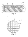
- a fixed abrasive article 10 that includes a fixed abrasive element 14 in the form of a layer disposed on a subpad 2 that includes a relatively more rigid element 34 disposed between the fixed abrasive element 14 and a relatively more resilient element 26.
- the fixed abrasive element 14 is bonded to the rigid element 34 through an adhesive composition 24.
- the rigid element 34 is bonded to the resilient element 26 through an adhesive composition 28.
- the abrasive article 10 further includes a layer of adhesive composition 30 disposed on the bottom surface of the resilient element 26 for use in attaching the abrasive article to a machine platen.
- the abrasive article 10 is suitable for modifying the surface of a substrate, e.g., the surface of a semiconductor wafer.
- the rigid element 34 includes a number of rigid segments 22 spaced apart from each other by grooves 32.
- the dimension of the rigid segments, the distance the rigid segments are spaced apart from each other and the shape of the rigid segments are selected to achieve a localized rigidity that is suitable for the substrate to be modified.
- the dimensions of the rigid segments 22 are selected to optimize localized planarity and global uniformity and to achieve a predetermined edge exclusion zone on a semiconductor wafer being modified by the abrasive article constructed with the rigid element.
- the size of the rigid segment 22 can be selected based upon the surface characteristics, e.g., die layout, e.g., repeat pattern of the die, and die size relative to the desired edge exclusion zone, of the semiconductor wafer being modified therewith.
- the footprint of the rigid segment is no greater than the desired maximum edge exclusion such that the pressure exerted by a rigid segment that does not extend beyond the edge of the semiconductor wafer is not affected by the proximity of the rigid segment to the edge of the semiconductor wafer.
- the rigid segments 22 are also preferably dimensioned to provide a neighborhood of localized rigidity that approximates or is slightly larger than the footprint of an individual die or repeating lithographic pattern on the semiconductor wafer to be modified.
- the rigid segments are from about 0.5 to about 4 times the size of the smallest dimension of the die being polished.
- Useful rigid segments have a cross-sectional area taken in a plane of the segment that is parallel to the working surface of the abrasive article that is no greater than about 400 mm 2 .
- the rigid segments 22 are separated from one another by grooves 32 extending into the depth of a rigid element 34 and across the surface of the rigid element 34.
- the grooves 32 render the rigid element 34 relatively more flexible than the rigid element without the grooves such that the rigid element 34 as a whole is capable of conforming to the surface of a semiconductor wafer while the individual segments 22 remain rigid.
- the depth to which the grooves 32 extend into the rigid element 34 can vary.
- the rigid element can include, e.g., grooves 32 that extend into the rigid element 34, through the rigid element 34, through the rigid element 34 and into the underlying relatively more resilient element 26, through the rigid element 34 and through the underlying relatively more resilient element 26, and combinations thereof.
- the abrasive article construction becomes more flexible.
- the grooves extend through the rigid element 34 to provide rigid segments 22 that sit on the resilient element 26 and move substantially independently of the other rigid segments so as to allow the rigid element to conform to the surface of the semiconductor wafer while maintaining localized planarization; more preferably the movement of one rigid segment is not imparted or transferred to any of its neighboring segments.
- Fig. 1 illustrates an abrasive article 10 that includes grooves 32 extending into the rigid element 34.
- Fig. 3 illustrates grooves 32a passing through the rigid element 34 such that rigid segments 22a are independently suspended on the resilient element 26.
- Fig. 5 illustrates grooves 32b passing through the rigid element 34 and extending into the resilient element 26 and grooves 32c passing through the rigid element 34 and through the resilient element 26.
- Fig. 6 illustrates an abrasive article 40 that includes grooves 42a extending into the rigid element 34 from the top surface 43 of the rigid element 34 and grooves 42b extending into the rigid element 34 from the bottom surface 44 of the rigid element 34.
- the width of the grooves i.e., the spacing between segments, is selected based on the desired subpad flexibility and conformity.
- the width of the groove can be increased such that the segments are completely separated or substantially completely separated from each other.
- the nominal pressure at the wafer surface is controlled by imposing pressure on the back side of the wafer.
- the fraction of the total plan area occupied by the rigid segments is reduced. Since pressure is transmitted through the rigid segments, the total force exerted on the back side of the wafer is transmitted through a smaller total area relative to an unsegmented rigid element and the nominal pressure at the tops of the rigid segments, where material removal processes occur, is increased.
- the nominal pressure exerted on the segments and transferred to the semiconductor wafer can be controlled by changing the percentage of segments, e.g., if 50% of the plan area of the rigid element includes segments, the average pressure at the process surface increases by a factor of 2 over the nominal applied pressure.
- the effect of groove width on the process pressure is another factor to be considered in choosing groove width.
- the shape of the groove is defined by at least one side wall, e.g., a continuous arcuate side wall, and can be defined by two or more side walls including, e.g., two substantially parallel side walls, two diverging or converging side walls, and two side walls separated by the bottom wall of the groove.
- the grooves 32 can be arranged to define rigid segments having a variety of shapes including, e.g., circular, elliptical, polygonal, e.g., triangles, rectangles, hexagons, and octagons.
- the rigid segments can be in a variety of forms including, e.g., parallelepiped, cylindrical, conical, pyramidal, frusto-pyramidal, frusto-conical, frusto-hemispherical, and other frusta.
- Fig. 2 illustrates an array of grooves positioned at right angles to each other to define generally square rigid segments 22.
- the rigid segments 22 can also be shaped to interdigitate with one another as illustrated, e.g., in Fig. 7.
- Fig. 4a illustrates a rigid segment 22a in which the union 76a of a side wall 72a and the top wall 74a, i.e., the surface of the rigid segment that is closest to the abrasive element, of a rigid segment 22a form a 90° angle.
- the union 76 of the side walls 72 and the top wall 74 can also be other than a 90° angle including, e.g., a slanted or curved union.
- Fig. 4b illustrates a rigid segment 22b in which the union 76b between the side wall 72b and the top wall 74b is tapered, i.e., beveled.
- 4c illustrates a rigid segment in which the union 76c between the side walls 72c and the top wall 74c is rounded. Tapering or rounding one or more of the corners of the rigid segment at the top of the rigid segment provides for a relatively smoother transition for the semiconductor wafer moving across the surface of an abrasive article constructed therewith.
- Fig. 9 illustrates an embodiment in which the rigid element 54 includes a number of rigid segments 64a, 64b and 64c having different dimensions (e.g., cross-sectional area), spacing or shapes, and located in different regions 68a, 68b and 68c on the rigid element.
- the rigid element 54 includes a number of rigid segments 64a, 64b and 64c having different dimensions (e.g., cross-sectional area), spacing or shapes, and located in different regions 68a, 68b and 68c on the rigid element.
- the rigid element is preferably in the form of a layer that is coextensive with the abrasive element and the abrasive element preferably extends across the rigid segments and the spaces, i.e., the grooves, between the rigid segments.
- the segmented rigid element can be in a variety of forms including, e.g., a round disk and a continuous web, e.g., a belt.
- the material of the segmented rigid element is selected in combination with the material of the resilient element and rigid segment geometry to provide an abrasive construction that exhibits uniform material removal across the surface of the substrate to be modified, and good planarization of lithographically produced features.
- Preferred rigid materials have a Young's Modulus value of at least about 100 MPa.
- the Young's Modulus of the rigid element is determined using the appropriate ASTM test in the plane defined by the two major surfaces of the material at room temperature (20°C to 25°C).
- the Young's Modulus of an organic polymer e.g.. plastics or reinforced plastics
- ASTM D638-84 Standard Test Methods for Tensile Properties of Plastics
- ASTM D882-88 Standard Tensile Properties of Thin Plastic Sheet
- the Young's Modulus of a metal is measured according to ASTM E345-93 (Standard Test Methods of Tension Testing of Metallic Foil).
- ASTM E345-93 Standard Test Methods of Tension Testing of Metallic Foil.
- the Young's Modulus of the overall element i.e., the laminate modulus
- the Young's Modulus of the overall element can be measured using the test for the highest modulus material.
- the thickness of the rigid element is selected based upon its modulus and the desired properties of the resulting abrasive construction. Useful thickness values for the rigid element range from about 0.075 mm to about 1.5 mm. Often as the Young's Modulus for a material increases, the required thickness of the material decreases.
- the rigid element can be made from a variety of materials including, e.g., organic polymers, inorganic polymers, ceramics, metals, composites of organic polymers, and combinations thereof.
- Suitable organic polymers can be thermoplastic or thermoset.
- Suitable thermoplastic materials include, polycarbonates, polyesters, polyurethanes, polystyrenes, polyolefins, polyperfluoroolefins, polyvinyl chlorides, and copolymers thereof.
- Suitable thermosetting polymers include, e.g., epoxies, polyimides, polyesters, and copolymers thereof (i.e., polymers containing at least two different monomers including, e.g., terpolymers and tetrapolymers).
- the polymer of the rigid element may be reinforced.
- the reinforcement can be in the form of fibers or particulate material. Suitable materials for use as reinforcement include, e.g., organic or inorganic fibers (e.g., continuous or staple), silicates, e.g., mica or talc, silica-based materials, e.g., sand and quartz, metal particulates, glass, metallic oxides and calcium carbonate, or a combination thereof.
- Metal sheets can also be used as the rigid element. Suitable metals include, e.g., aluminum, stainless steel and copper.
- Particularly useful rigid materials include poly(ethylene terephthalate), polycarbonate, glass fiber reinforced epoxy boards, aluminum, stainless steel and IC 1000 (available from Rodel, Inc., Newark, Del.).
- the resilient element 26 can be a continuous layer or a discontinuous layer and can be divided into segments as described above with respect to the segmenting of the rigid substrate as illustrated in Fig. 5.
- the resilient element can include one layer of material or a number of layers of the same or different materials, provided that the mechanical behavior of the layered element is acceptable for the desired application.
- the resilient element is preferably capable of undergoing compression during a surface modification process.
- the resiliency, i.e., the stiffness in compression and elastic rebound, of the resilient element is related to the modulus of the material of the resilient element in the thickness direction and is also affected by the thickness of the resilient element.
- the choice of material for the resilient element, as well as the thickness of the resilient element, will vary depending on the variables in the process including, e.g., the composition of the workpiece surface and fixed abrasive element, the shape and initial flatness of the workpiece surface, the type of apparatus used for modifying the surface (e.g.. planarizing the surface), and the pressures used in the modification process.
- Preferred resilient materials including, e.g., the overall resilient element itself, have a Young's Modulus value of less than about 100 MPa, more preferably less than about 50 MPa.
- Dynamic compressive testing of resilient materials can be used to measure the Young's Modulus (often referred to as the storage or elastic modulus) in the thickness direction of the resilient material.
- ASTM D5024-94 Standard Test Methods for Measuring the Dynamic Mechanical Properties of Plastics in Compression
- the Young's Modulus of the resilient element is determined according to ASTM D5024-94 in the thickness direction of the material at 20°C and 0.1 Hz with a preload equal to the nominal CMP process pressure.
- Suitable resilient materials can also be selected by additionally evaluating their stress relaxation. Stress relaxation is evaluated by deforming a material and holding it in the deformed state while the force or stress needed to maintain deformation is measured. Suitable resilient materials (or the overall resilient element) preferably retain at least about 60% (more preferably at least about 70%) of the initially applied stress, after 120 seconds. This is referred to herein, as the "remaining stress” and is determined by first compressing a sample of material no less than 0.5 mm thick at a rate of 25.4 mm/minute until an initial stress of 83 kPa is achieved at room temperature (20°C-25°C) and measuring the remaining stress after 2 minutes.
- the resilient element can include a wide variety of resilient materials.
- useful resilient materials include organic polymers, e.g., thermoplastic or thermoset polymers, that may be elastomeric.
- Suitable organic polymers include those organic polymers that are foamed or blown to produce porous organic structures, i.e., foams.
- foams may be prepared from natural or synthetic rubber or other thermoplastic elastomers, e.g., polyolefins, polyesters, polyamides, polyurethanes, and copolymers thereof.
- Suitable synthetic thermoplastic elastomers include, e.g., chloroprene rubbers, ethylene/propylene rubbers, butyl rubbers, polybutadienes, polyisoprenes, EPDM polymer, polyvinyl chlorides, polychloroprenes, styrene-butadiene copolymers, and styrene-isoprene copolymers, and mixtures thereof.
- a useful resilient material is a copolymer of polyethylene and ethylvinyl acetate in the form of foam.
- Other useful resilient materials include polyurethane impregnated felt-based materials, nonwoven or woven fiber mats that include, e.g., polyolefin, polyester or polyamide fibers, and resin impregnated woven and nonwoven materials.
- the fibers may be of finite length (i.e., staple) or substantially continuous in the fiber mat.
- Examples of useful commercially available resilient materials include poly(ethylene-co-vinyl acetate) foams available under the trade designations 3M SCOTCH brand CUSHIONMOUNT Plate Mounting Tape 949 double-coated high density elastomeric foam tape (Minnesota Mining and Manufacturing Company, St. Paul, MN), EO EVA foam (Voltek, Lawrence, MA), EMR 1025 polyethylene foam (Sentinel Products, Hyannis, N.J.), HD200 polyurethane foam (Illbruck, Inc. Minneapolis, MN), MC8000 and MC8000EVA foams (Sentinel Products), SUBA IV Impregnated Nonwoven (Rodel, Inc., Newark, DE).
- poly(ethylene-co-vinyl acetate) foams available under the trade designations 3M SCOTCH brand CUSHIONMOUNT Plate Mounting Tape 949 double-coated high density elastomeric foam tape (Minnesota Mining and Manufacturing Company, St. Paul, MN),
- pads having rigid and resilient elements that are used in slurry polishing operations are also suitable.
- An example of such a pad is available under the trade designation IC1000-SUBA IV from Rodel, Inc. (Newark, Delaware).
- the abrasive element 14 of Figs. 1 and 3 includes a plurality of abrasive particles in fixed position in a binder, optionally bonded to a support 18, e.g., a backing.
- the abrasive element is a textured, three-dimensional, fixed abrasive element that includes a number of composites 16 of abrasive particles disposed in a binder and bonded to a backing 18.
- the abrasive composites 16 of the textured, three-dimensional, fixed abrasive element can be arranged in a pattern, randomly and combinations thereof. Examples of useful textured, three-dimensional, fixed abrasive elements are disclosed in U.S.-A-5,958,794 and WO-A- 98/49723.
- the fixed abrasive element with its abrasive particles disposed in a binder has a relatively high modulus.
- the backing of the fixed abrasive element may have high in plane modulus, yet be sufficiently thin to be flexible.
- the in plane stiffness and flexibility of the fixed abrasive element is preferably sufficient to enable the fixed abrasive element to be used in the form of a web including, e.g., being capable of being wound in a roll on take up and unwind rollers.
- the abrasive element can be in the form of a layer extending across the rigid segments.
- the abrasive element can also be coextensive with individual rigid segments.
- Useful abrasive article constructions include, e.g., disc, web and multiple web constructions.
- the components of the abrasive article can be maintained in fixed relation to each other.
- useful means for maintaining the various components of the abrasive article in fixed relation to each another include, e.g., adhesive compositions, mechanical fastening devices, tie layers, and combinations thereof.
- the components can also be bonded together through processes including, e.g., thermal bonding, ultrasonic welding, microwave-activated bonding, coextrusion of at least two components of the abrasive article, and combinations thereof.
- Useful adhesives include, e.g., pressure sensitive adhesives, hot melt adhesives and glue.
- Suitable pressure sensitive adhesives include a wide variety of pressure sensitive adhesives including, e.g., natural rubber-based adhesives, (meth)acrylate polymers and copolymers, AB or ABA block copolymers of thermoplastic rubbers, e.g., styrene/butadiene or styrene/isoprene block copolymers available under the trade designation KRATON (Shell Chemical Co., Houston, Texas) or polyolefins.
- Suitable hot melt adhesives include, e.g., polyester, ethylene vinyl acetate (EVA), polyamides, epoxies, and combinations thereof.
- the adhesive preferably has sufficient cohesive strength and peel resistance to maintain the components of the fixed abrasive article in fixed relation to each other during use and is resistant to chemical degradation under conditions of use.
- the abrasive article can also include a variety of mechanisms for attachment to a machine platen, e.g., a machine platen used in chemical mechanical planarization, including, e.g., adhesive or mechanical means including, e.g., placement pins, retaining ring, tension, vacuum or a combination thereof.
- the abrasive article can be adapted for use in many types of semiconductor wafer planarizing machines including those suitable for use with polishing pads and loose abrasive slurries.
- An example of a suitable commercially available machine is a Chemical Mechanical Planarization (CMP) machine available from Applied Materials, Inc. (Santa Clara, CA).
- CMP Chemical Mechanical Planarization
- At least one component of the abrasive article including, e.g., the resilient element, the abrasive element, the rigid element or a combination thereof, can also be moveable relative to another component either during or before and after wafer surface modification.
- This arrangement may be desirable for a variety of purposes including, e.g., introducing a fresh fixed abrasive surface and maintaining stable web properties (including, e.g., the level of resiliency of the resilient element and the abrasive nature of the abrasive element) from wafer to wafer.
- Fig. 8 illustrates an apparatus 50 for modifying a substrate that includes a number of webs 52, 54, 56 where each web extends between an unwind roller 51, 55, and 59, respectively, and a take-up roller 53, 57 and 61, respectively.
- Web 52 includes an abrasive element 58 of fixed abrasive composites 60 bonded to a backing 62.
- Web 54 includes a number of rigid segments 64. Web 54 is capable of being rolled up due to the reduced flexural rigidity of the rigid element that results from segmenting the rigid element.
- Web 56 includes a resilient element 66.
- the individual webs 52, 54, 56 can move independently of one another, e.g., the abrasive web 52 is capable of moving independently of the segmented rigid web 54 and the resilient web 56. Individual webs 52, 54, 56 can also move at the same speed or different speeds and at least one web can remain stationary while another web moves. Alternatively, at least two of the webs 52, 54, 56 can be in a fixed relationship to each other, e.g., bonded together, and capable of moving as a single unit.
- the individual webs can be held stationary using mechanisms that include, e.g., exerting tension using the wind and unwind rollers, applying forces at the edges of the webs by a variety of mechanisms including, e.g., vacuum hold-down to the machine platen, and combinations thereof.
- the individual webs 52, 54, 56 can also move independently of or simultaneously with one another to provide an abrasive article that includes one or more regions exhibiting different properties to achieve an abrasive article having desired surface modifying properties.
- the apparatus 50 may include an abrasive web 58 that includes regions in which the textured, fixed abrasive composites 60 have a more aggressive abrading property, and regions in which the textured, fixed abrasive composites 60 have a less aggressive abrading property, which may result from, e.g., the abrasive web fabrication process or use in a previous polishing operation.
- the mechanism that controls the movement of the semiconductor wafer relative to the abrasive article can be preprogrammed such that the wafer contacts the various regions of the abrasive article according to a predetermined surface modifying sequence to achieve a desired surface modification.
- the abrasive article and apparatus can be used in a variety of semiconductor wafer -A-surface modifying processes including those methods described in, e.g., U.S.-A-5,958,794 and US-A-6,007,407.
Landscapes
- Engineering & Computer Science (AREA)
- Mechanical Engineering (AREA)
- Physics & Mathematics (AREA)
- Condensed Matter Physics & Semiconductors (AREA)
- General Physics & Mathematics (AREA)
- Manufacturing & Machinery (AREA)
- Computer Hardware Design (AREA)
- Microelectronics & Electronic Packaging (AREA)
- Power Engineering (AREA)
- Polishing Bodies And Polishing Tools (AREA)
- Mechanical Treatment Of Semiconductor (AREA)
- Finish Polishing, Edge Sharpening, And Grinding By Specific Grinding Devices (AREA)
Claims (28)
- Article à abrasif comprenant :caractérisé parun élément abrasif fixe (14,58) comprenant une pluralité de particules abrasives (16,60) ; etun élément élastique (26) ;une pluralité de segments rigides (22, 22a, 22b, 22c, 64, 64a, 64b, 64c) disposés entre ledit élément abrasif fixe (14) et ledit élément élastique (26).
- Article selon la revendication 1, dans lequel lesdits segments rigides (22, 22a, 22b, 22c, 64, 64a, 64b, 64c) sont attachés les uns aux autres.
- Article selon la revendication 2, dans lequel lesdits segments rigides (22, 22a, 22b, 22c, 64, 64a, 64b, 64c) s'étendent à partir d'un support commun et sont définis au moins en partie par une pluralité de rainures intersectées (32, 32a, 32b, 32c) dans ledit support.
- Article selon la revendication 1, dans lequel lesdits segments rigides (22, 22a, 22b, 22c, 64, 64a, 64b, 64c) sont détachés les uns des autres.
- Article selon l'une quelconque des revendications 1 à 4, dans lequel ledit élément abrasif fixe (14, 58) comprend une couche discontinue.
- Article selon l'une quelconque des revendications 1 à 5, dans lequel ledit élément abrasif fixe (14, 58) comprend une pluralité de segments abrasifs fixes, chaque segment abrasif fixe étant de même étendue que l'un desdits segments rigides (22, 22a, 22b, 22c, 64, 64a, 64b, 64c).
- Article selon l'une quelconque des revendications 1 à 6, dans lequel ledit élément abrasif fixe (14, 58) s'étend de façon continue à travers une pluralité desdits segments rigides (22, 22a, 22b, 22c, 64, 64a, 64b, 64c).
- Article selon l'une quelconque des revendications 1 à 7, dans lequel ledit élément abrasif fixe (14, 58) est lié auxdits segments rigides (22, 22a, 22b, 22c, 64, 64a, 64b, 64c).
- Article selon l'une quelconque des revendications 1 à 8, dans lequel lesdits segments rigides (22, 22a, 22b, 22c, 64, 64a, 64b, 64c) sont liés audit élément élastique (26).
- Article selon l'une quelconque des revendications 1 à 9, dans lequel ledit élément élastique (26) comprend une pluralité de segments élastiques.
- Article selon la revendication 10, dans lequel lesdits segments élastiques sont liés auxdits segments rigides (22, 22a, 22b, 22c, 64, 64a, 64b, 64c).
- Article selon l'une quelconque des revendications 1 à 11, dans lequel ledit élément abrasif fixe (14, 58) comprend un élément abrasif fixe texturé, en trois dimensions.
- Article selon l'une quelconque des revendications 1 à 12, dans lequel ledit élément abrasif fixe (14, 58) comprend une pluralité de composites abrasifs fixes en trois dimensions (16, 60).
- Article selon l'une quelconque des revendications 1 à 13, dans lequel lesdits segments rigides (22, 22a, 22b, 22c, 64, 64a, 64b, 64c) comprennent une surface supérieure (74, 74a, 74b, 74c), une paroi latérale (72, 72a, 72b, 72c) et une arête. (76, 76a, 76b, 76c) disposée entre la surface supérieure (74, 74a, 74b, 74c) et la paroi latérale (72, 72a, 72b, 72c), ladite arête (76, 76a, 76b, 76c) étant biseautée.
- Article selon l'une quelconque des revendications 1 à 13, dans lequel lesdits segments rigides (22, 22a, 22b, 22c, 64, 64a, 64b, 64c) comprennent une surface supérieure (74, 74a, 74b, 74c), une paroi latérale (72, 72a, 72b, 72c) et une arête (76, 76a, 76b, 76c) disposée entre la surface supérieure (74, 74a, 74b, 74c) et la paroi latérale (72, 72a, 72b, 72c), ladite arête (76, 76a, 76b, 76c) étant courbe.
- Article selon l'une quelconque des revendications 1 à 15, dans lequel lesdits segments rigides sont interdigités.
- Article selon l'une quelconque des revendications 1 à 16, dans lequel lesdits segments rigides (22, 22a, 22b, 22c, 64, 64a, 64b, 64c) sont sélectionnés dans le groupe constitué de formes pyramidales, coniques, cylindriques, de troncs de cônes, de troncs de pyramides, de troncs d'hémisphères, et d'autres troncs.
- Article selon l'une quelconque des revendications 1 à 17, dans lequel lesdits segments rigides (22, 22a, 22b, 22c, 64, 64a, 64b, 64c) ont une surface de section transversale, mesurée dans un plan du segment qui est parallèle à la surface abrasive, ne dépassant pas 400 mm2.
- Article selon l'une quelconque des revendications 1 à 18, dans lequel l'article à abrasif est capable de s'adapter à la courbure d'une surface d'une tranche semi-conductrice et d'être rigide par rapport à une pastille présente sur la surface de la tranche semi-conductrice.
- Dispositif pour modifier la surface d'une tranche semi-conductrice, ledit dispositif comprenant l'article à abrasif selon l'une quelconque des revendications 1 à 19.
- Dispositif selon la revendication 20, comprenant en outreune première feuille (52) comprenant ledit élément abrasif fixe (58) ;une deuxième feuille (54) comprenant ladite pluralité de segments rigides (64) ; etune troisième feuille (56) comprenant ledit élément élastique (66).
- Dispositif selon la revendication 21, dans lequel ladite première feuille (52) et ladite deuxième feuille (54) ou ladite deuxième feuille (54) et ladite troisième feuille (56) ou ladite première feuille (52) et ladite troisième feuille (56) peuvent être déplacées les unes par rapport aux autres.
- Dispositif selon la revendication 21, dans lequel ladite première feuille (52), ladite deuxième feuille (54) et ladite troisième feuille (56) peuvent être déplacées les unes par rapport aux autres.
- Dispositif selon la revendication 21, comprenant en outre une feuille (54) comprenant :une première zone (68a) comprenant une première pluralité de segments rigides (64a) ayant une première surface de section transversale ; etune deuxième zone (68b, 68c) comprenant une deuxième pluralité de segments rigides (64b, 64c) ayant une deuxième surface de section transversale ;ladite première surface de section transversale étant différente de ladite deuxième surface de section transversale.
- Dispositif selon l'une quelconque des revendications 20 à 24, dans lequel ladite couche rigide comprend un matériau sélectionné dans le groupe constitué du métal et du plastique.
- Méthode de modification de la surface d'une tranche semi-conductrice, ladite méthode comprenant :la mise en contact de l'article à abrasif (10, 20, 40, 50) selon l'une quelconque des revendications 1 à 19 avec une tranche semi-conductrice ; etle déplacement de ladite tranche semi-conductrice et dudit article à abrasif (10, 20, 40, 50) l'un par rapport à l'autre.
- Méthode selon la revendication 26, comprenant en outre :la mise en contact d'une première zone de l'article à abrasif (10, 20, 40, 50) avec une tranche semi-conductrice, ladite première zone comprenant une première pluralité de segments rigides (64a) ayant une première surface de section transversale ;le déplacement de ladite tranche semi-conductrice et dudit article à abrasif fixe (10, 20, 40, 50) l'un par rapport à l'autre ;la mise en contact d'une deuxième zone de l'article à abrasif (10, 20, 40, 50) avec la tranche semi-conductrice, ladite deuxième zone comprenant une deuxième pluralité desdits segments rigides (64b, 64c) ayant une deuxième dimension de section transversale ; etle déplacement de ladite tranche semi-conductrice et dudit article à abrasif fixe (10, 20, 40, 50) l'un par rapport à l'autre.
- Méthode selon la revendication 26 ou 27, dans laquelle ledit article à abrasif (10, 20, 40, 50) comprend en outre une feuille (54), ladite feuille (54) comprenant ladite pluralité de segments rigides (64, 64a, 64b, 64c), ladite méthode comprenant en outre le déplacement de ladite feuille (54) d'une première position à une deuxième position.
Applications Claiming Priority (3)
| Application Number | Priority Date | Filing Date | Title |
|---|---|---|---|
| US09/784,667 US6632129B2 (en) | 2001-02-15 | 2001-02-15 | Fixed abrasive article for use in modifying a semiconductor wafer |
| US784667 | 2001-02-15 | ||
| PCT/US2001/019522 WO2002074490A1 (fr) | 2001-02-15 | 2001-06-19 | Article a abrasif fixe destine a la modification d'une tranche semi-conductrice |
Publications (2)
| Publication Number | Publication Date |
|---|---|
| EP1360034A1 EP1360034A1 (fr) | 2003-11-12 |
| EP1360034B1 true EP1360034B1 (fr) | 2005-12-07 |
Family
ID=25133157
Family Applications (1)
| Application Number | Title | Priority Date | Filing Date |
|---|---|---|---|
| EP01948459A Expired - Lifetime EP1360034B1 (fr) | 2001-02-15 | 2001-06-19 | Article a abrasif fixe destine a la modification d'une tranche semi-conductrice |
Country Status (8)
| Country | Link |
|---|---|
| US (2) | US6632129B2 (fr) |
| EP (1) | EP1360034B1 (fr) |
| JP (1) | JP2004524697A (fr) |
| KR (1) | KR100742794B1 (fr) |
| CN (1) | CN1289263C (fr) |
| AT (1) | ATE311958T1 (fr) |
| DE (1) | DE60115710T2 (fr) |
| WO (1) | WO2002074490A1 (fr) |
Families Citing this family (59)
| Publication number | Priority date | Publication date | Assignee | Title |
|---|---|---|---|---|
| US7516536B2 (en) * | 1999-07-08 | 2009-04-14 | Toho Engineering Kabushiki Kaisha | Method of producing polishing pad |
| US6869343B2 (en) * | 2001-12-19 | 2005-03-22 | Toho Engineering Kabushiki Kaisha | Turning tool for grooving polishing pad, apparatus and method of producing polishing pad using the tool, and polishing pad produced by using the tool |
| US7192340B2 (en) * | 2000-12-01 | 2007-03-20 | Toyo Tire & Rubber Co., Ltd. | Polishing pad, method of producing the same, and cushion layer for polishing pad |
| US7070480B2 (en) * | 2001-10-11 | 2006-07-04 | Applied Materials, Inc. | Method and apparatus for polishing substrates |
| US6908366B2 (en) | 2003-01-10 | 2005-06-21 | 3M Innovative Properties Company | Method of using a soft subpad for chemical mechanical polishing |
| KR101018942B1 (ko) | 2003-01-10 | 2011-03-02 | 쓰리엠 이노베이티브 프로퍼티즈 컴파니 | 화학 기계적 평탄화 적용을 위한 패드 구조물 |
| KR100504941B1 (ko) * | 2003-05-09 | 2005-08-02 | 매그나칩 반도체 유한회사 | 화학적 기계적 연마 장치 |
| US7435161B2 (en) * | 2003-06-17 | 2008-10-14 | Cabot Microelectronics Corporation | Multi-layer polishing pad material for CMP |
| US6997777B2 (en) * | 2003-06-17 | 2006-02-14 | Cabot Microelectronics Corporation | Ultrasonic welding method for the manufacture of a polishing pad comprising an optically transmissive region |
| US6884156B2 (en) * | 2003-06-17 | 2005-04-26 | Cabot Microelectronics Corporation | Multi-layer polishing pad material for CMP |
| JP4484466B2 (ja) * | 2003-07-10 | 2010-06-16 | パナソニック株式会社 | 研磨方法およびその研磨方法に用いる粘弾性ポリッシャー |
| US7160178B2 (en) * | 2003-08-07 | 2007-01-09 | 3M Innovative Properties Company | In situ activation of a three-dimensional fixed abrasive article |
| US20050054277A1 (en) * | 2003-09-04 | 2005-03-10 | Teng-Chun Tsai | Polishing pad and method of polishing wafer |
| US7654885B2 (en) * | 2003-10-03 | 2010-02-02 | Applied Materials, Inc. | Multi-layer polishing pad |
| US8066552B2 (en) | 2003-10-03 | 2011-11-29 | Applied Materials, Inc. | Multi-layer polishing pad for low-pressure polishing |
| DE102004007747B3 (de) * | 2004-02-18 | 2004-12-23 | Jöst, Peter | Schleifbandträger und Schleifbandanordnung |
| US6951509B1 (en) * | 2004-03-09 | 2005-10-04 | 3M Innovative Properties Company | Undulated pad conditioner and method of using same |
| US7485028B2 (en) | 2004-03-19 | 2009-02-03 | Saint-Gobain Performance Plastics Corporation | Chemical mechanical polishing retaining ring, apparatuses and methods incorporating same |
| US7086939B2 (en) * | 2004-03-19 | 2006-08-08 | Saint-Gobain Performance Plastics Corporation | Chemical mechanical polishing retaining ring with integral polymer backing |
| US20050227590A1 (en) * | 2004-04-09 | 2005-10-13 | Chien-Min Sung | Fixed abrasive tools and associated methods |
| US8075372B2 (en) * | 2004-09-01 | 2011-12-13 | Cabot Microelectronics Corporation | Polishing pad with microporous regions |
| JP2006127606A (ja) * | 2004-10-27 | 2006-05-18 | Hitachi Global Storage Technologies Netherlands Bv | 磁気ディスクの製造方法 |
| US20060150992A1 (en) * | 2005-01-07 | 2006-07-13 | Nevakshonoff Michael G | Device for sanding buffing or grinding elongate objects |
| US7875091B2 (en) * | 2005-02-22 | 2011-01-25 | Saint-Gobain Abrasives, Inc. | Rapid tooling system and methods for manufacturing abrasive articles |
| US7524345B2 (en) * | 2005-02-22 | 2009-04-28 | Saint-Gobain Abrasives, Inc. | Rapid tooling system and methods for manufacturing abrasive articles |
| US7867302B2 (en) * | 2005-02-22 | 2011-01-11 | Saint-Gobain Abrasives, Inc. | Rapid tooling system and methods for manufacturing abrasive articles |
| US7179159B2 (en) * | 2005-05-02 | 2007-02-20 | Applied Materials, Inc. | Materials for chemical mechanical polishing |
| KR100655584B1 (ko) * | 2005-07-08 | 2006-12-08 | 동부일렉트로닉스 주식회사 | 실접촉 면적이 서로 다른 영역을 하나의 패드로 구현한고정입자 패드 및 및 그 제조방법 |
| US7618306B2 (en) * | 2005-09-22 | 2009-11-17 | 3M Innovative Properties Company | Conformable abrasive articles and methods of making and using the same |
| US20070066186A1 (en) * | 2005-09-22 | 2007-03-22 | 3M Innovative Properties Company | Flexible abrasive article and methods of making and using the same |
| CN101244535B (zh) * | 2006-02-15 | 2012-06-13 | 应用材料公司 | 抛光仓 |
| TWI287486B (en) | 2006-05-04 | 2007-10-01 | Iv Technologies Co Ltd | Polishing pad and method thereof |
| US20080274674A1 (en) * | 2007-05-03 | 2008-11-06 | Cabot Microelectronics Corporation | Stacked polishing pad for high temperature applications |
| WO2009058463A1 (fr) * | 2007-10-31 | 2009-05-07 | 3M Innovative Properties Company | Composition, méthode et procédé de polissage d'une galette |
| TWI387508B (zh) * | 2008-05-15 | 2013-03-01 | 3M Innovative Properties Co | 具有終點窗孔之拋光墊及使用其之系統及方法 |
| KR20110019442A (ko) * | 2008-06-26 | 2011-02-25 | 쓰리엠 이노베이티브 프로퍼티즈 캄파니 | 다공성 요소를 구비한 연마 패드 및 이 연마 패드의 제작 방법 및 이용 방법 |
| US8662962B2 (en) * | 2008-06-30 | 2014-03-04 | 3M Innovative Properties Company | Sandpaper with non-slip coating layer and method of using |
| CN102131887B (zh) * | 2008-07-03 | 2013-07-31 | 3M创新有限公司 | 固定磨料颗粒和由其制得的制品 |
| JP5450622B2 (ja) * | 2008-07-18 | 2014-03-26 | スリーエム イノベイティブ プロパティズ カンパニー | 浮遊要素を備えた研磨パッド、その製造方法及び使用方法 |
| KR101007134B1 (ko) * | 2009-06-05 | 2011-01-10 | 엘지이노텍 주식회사 | 조명 장치 |
| DE102009030297B3 (de) * | 2009-06-24 | 2011-01-20 | Siltronic Ag | Verfahren zum Polieren einer Halbleiterscheibe |
| DE102009030294B4 (de) * | 2009-06-24 | 2013-04-25 | Siltronic Ag | Verfahren zur Politur der Kante einer Halbleiterscheibe |
| KR20120112662A (ko) * | 2009-12-30 | 2012-10-11 | 쓰리엠 이노베이티브 프로퍼티즈 컴파니 | 유기 미립자 로딩된 폴리싱 패드 및 이를 제조 및 사용하는 방법 |
| US9205530B2 (en) | 2010-07-07 | 2015-12-08 | Seagate Technology Llc | Lapping a workpiece |
| KR20140018880A (ko) * | 2011-01-26 | 2014-02-13 | 쓰리엠 이노베이티브 프로퍼티즈 컴파니 | 복제된 미세구조화 배킹을 갖는 연마재 물품 및 그것을 이용하는 방법 |
| CN102672548A (zh) * | 2011-11-08 | 2012-09-19 | 刘广庆 | 一种有机涂层研磨工艺 |
| US9649742B2 (en) * | 2013-01-22 | 2017-05-16 | Nexplanar Corporation | Polishing pad having polishing surface with continuous protrusions |
| JP6279309B2 (ja) * | 2013-12-20 | 2018-02-14 | スリーエム イノベイティブ プロパティズ カンパニー | 研磨用クッション、研磨装置、研磨方法、及び当該研磨方法により研磨された対象物を含む物品 |
| CN106376234B (zh) | 2014-05-02 | 2019-11-05 | 3M创新有限公司 | 间断的结构化磨料制品以及抛光工件的方法 |
| US10201886B2 (en) * | 2014-05-21 | 2019-02-12 | Fujibo Holdings, Inc. | Polishing pad and method for manufacturing the same |
| CN106181652A (zh) * | 2015-05-08 | 2016-12-07 | 蓝思科技股份有限公司 | 磨机的磨皮开槽方法及修复弯片玻璃的方法 |
| CN108472789B (zh) * | 2016-01-08 | 2020-06-05 | 阪东化学株式会社 | 研磨材 |
| US10259099B2 (en) * | 2016-08-04 | 2019-04-16 | Rohm And Haas Electronic Materials Cmp Holdings, Inc. | Tapering method for poromeric polishing pad |
| US10864612B2 (en) * | 2016-12-14 | 2020-12-15 | Taiwan Semiconductor Manufacturing Company, Ltd. | Polishing pad and method of using |
| TWI621501B (zh) * | 2017-01-06 | 2018-04-21 | 三芳化學工業股份有限公司 | 研磨墊及研磨裝置 |
| JP6883475B2 (ja) * | 2017-06-06 | 2021-06-09 | 株式会社荏原製作所 | 研磨テーブル及びこれを備える研磨装置 |
| CN112154377A (zh) * | 2018-05-22 | 2020-12-29 | Asml控股股份有限公司 | 用于原位夹具表面粗糙化的装置和方法 |
| US11331767B2 (en) | 2019-02-01 | 2022-05-17 | Micron Technology, Inc. | Pads for chemical mechanical planarization tools, chemical mechanical planarization tools, and related methods |
| JP7538397B2 (ja) | 2020-03-23 | 2024-08-22 | 富士紡ホールディングス株式会社 | 研磨パッド |
Family Cites Families (41)
| Publication number | Priority date | Publication date | Assignee | Title |
|---|---|---|---|---|
| US4576850A (en) | 1978-07-20 | 1986-03-18 | Minnesota Mining And Manufacturing Company | Shaped plastic articles having replicated microstructure surfaces |
| US4244775A (en) | 1979-04-30 | 1981-01-13 | Bell Telephone Laboratories, Incorporated | Process for the chemical etch polishing of semiconductors |
| US4374077A (en) | 1980-02-01 | 1983-02-15 | Minnesota Mining And Manufacturing Company | Process for making information carrying discs |
| US4712552A (en) * | 1982-03-10 | 1987-12-15 | William W. Haefliger | Cushioned abrasive composite |
| CH669138A5 (de) | 1982-11-22 | 1989-02-28 | Schweizer Schmirgel Schleif | Schleifmittel auf dehnbarer und flexibler unterlage. |
| US4588258A (en) | 1983-09-12 | 1986-05-13 | Minnesota Mining And Manufacturing Company | Cube-corner retroreflective articles having wide angularity in multiple viewing planes |
| US5183597A (en) | 1989-02-10 | 1993-02-02 | Minnesota Mining And Manufacturing Company | Method of molding microstructure bearing composite plastic articles |
| US5109638A (en) | 1989-03-13 | 1992-05-05 | Microsurface Finishing Products, Inc. | Abrasive sheet material with non-slip backing |
| US5020283A (en) | 1990-01-22 | 1991-06-04 | Micron Technology, Inc. | Polishing pad with uniform abrasion |
| US5177908A (en) | 1990-01-22 | 1993-01-12 | Micron Technology, Inc. | Polishing pad |
| US5127197A (en) * | 1991-04-25 | 1992-07-07 | Brukvoort Wesley J | Abrasive article and processes for producing it |
| US5230184A (en) | 1991-07-05 | 1993-07-27 | Motorola, Inc. | Distributed polishing head |
| US5212910A (en) * | 1991-07-09 | 1993-05-25 | Intel Corporation | Composite polishing pad for semiconductor process |
| US5287663A (en) | 1992-01-21 | 1994-02-22 | National Semiconductor Corporation | Polishing pad and method for polishing semiconductor wafers |
| US6022264A (en) | 1997-02-10 | 2000-02-08 | Rodel Inc. | Polishing pad and methods relating thereto |
| US5564965A (en) * | 1993-12-14 | 1996-10-15 | Shin-Etsu Handotai Co., Ltd. | Polishing member and wafer polishing apparatus |
| BR9506932A (pt) | 1994-02-22 | 1997-09-09 | Minnesota Mining & Mfg | Artigo abrasivo e processo para produzir o mesmo |
| US5489233A (en) | 1994-04-08 | 1996-02-06 | Rodel, Inc. | Polishing pads and methods for their use |
| US5607341A (en) | 1994-08-08 | 1997-03-04 | Leach; Michael A. | Method and structure for polishing a wafer during manufacture of integrated circuits |
| JPH10506579A (ja) | 1994-09-30 | 1998-06-30 | ミネソタ・マイニング・アンド・マニュファクチュアリング・カンパニー | 被覆研磨物品、その製造法及び使用方法 |
| US5575707A (en) | 1994-10-11 | 1996-11-19 | Ontrak Systems, Inc. | Polishing pad cluster for polishing a semiconductor wafer |
| EP0812456B1 (fr) * | 1995-03-02 | 2000-01-12 | Minnesota Mining And Manufacturing Company | Procede de texturation d'un substrat a l'aide d'un article abrasif structure |
| US5897424A (en) | 1995-07-10 | 1999-04-27 | The United States Of America As Represented By The Secretary Of Commerce | Renewable polishing lap |
| US5958794A (en) | 1995-09-22 | 1999-09-28 | Minnesota Mining And Manufacturing Company | Method of modifying an exposed surface of a semiconductor wafer |
| JPH0985631A (ja) * | 1995-09-28 | 1997-03-31 | Fuji Photo Film Co Ltd | 研磨体 |
| US5609517A (en) | 1995-11-20 | 1997-03-11 | International Business Machines Corporation | Composite polishing pad |
| TW349896B (en) | 1996-05-02 | 1999-01-11 | Applied Materials Inc | Apparatus and chemical mechanical polishing system for polishing a substrate |
| US5692950A (en) | 1996-08-08 | 1997-12-02 | Minnesota Mining And Manufacturing Company | Abrasive construction for semiconductor wafer modification |
| JPH10156705A (ja) | 1996-11-29 | 1998-06-16 | Sumitomo Metal Ind Ltd | 研磨装置および研磨方法 |
| CA2192880C (fr) * | 1996-12-13 | 2005-02-22 | Brian H. Parrott | Dispositifs de poncage et elements similaires pour l'enlevement de materiau |
| US5897930A (en) | 1996-12-31 | 1999-04-27 | Minnesota Mining And Manufacturing Company | Multiple embossed webs |
| TW479285B (en) | 1997-04-30 | 2002-03-11 | Minnesota Mining & Mfg | Method of modifying a wafer suited for semiconductor fabrication |
| WO1998050201A1 (fr) | 1997-05-09 | 1998-11-12 | Rodel Holdings, Inc. | Tampons a polir mosaiques et procedes afferents |
| DE19727104C2 (de) * | 1997-06-26 | 2000-07-20 | Ver Schmirgel & Maschf | Flexibler Schleifkörper und Verfahren zu seiner Herstellung |
| AU9122298A (en) | 1997-08-26 | 1999-03-16 | Ning Wang | A pad for chemical-mechanical polishing and apparatus and methods of manufacturethereof |
| JPH11156699A (ja) | 1997-11-25 | 1999-06-15 | Speedfam Co Ltd | 平面研磨用パッド |
| US6059850A (en) | 1998-07-15 | 2000-05-09 | 3M Innovative Properties Company | Resilient abrasive article with hard anti-loading size coating |
| US6206759B1 (en) * | 1998-11-30 | 2001-03-27 | Micron Technology, Inc. | Polishing pads and planarizing machines for mechanical or chemical-mechanical planarization of microelectronic-device substrate assemblies, and methods for making and using such pads and machines |
| US6217426B1 (en) | 1999-04-06 | 2001-04-17 | Applied Materials, Inc. | CMP polishing pad |
| US6234875B1 (en) | 1999-06-09 | 2001-05-22 | 3M Innovative Properties Company | Method of modifying a surface |
| US6612917B2 (en) * | 2001-02-07 | 2003-09-02 | 3M Innovative Properties Company | Abrasive article suitable for modifying a semiconductor wafer |
-
2001
- 2001-02-15 US US09/784,667 patent/US6632129B2/en not_active Expired - Lifetime
- 2001-06-19 CN CNB018226604A patent/CN1289263C/zh not_active Expired - Fee Related
- 2001-06-19 EP EP01948459A patent/EP1360034B1/fr not_active Expired - Lifetime
- 2001-06-19 WO PCT/US2001/019522 patent/WO2002074490A1/fr active IP Right Grant
- 2001-06-19 DE DE60115710T patent/DE60115710T2/de not_active Expired - Lifetime
- 2001-06-19 KR KR1020037010726A patent/KR100742794B1/ko not_active IP Right Cessation
- 2001-06-19 JP JP2002573189A patent/JP2004524697A/ja active Pending
- 2001-06-19 AT AT01948459T patent/ATE311958T1/de not_active IP Right Cessation
-
2003
- 2003-09-12 US US10/662,084 patent/US7329171B2/en not_active Expired - Fee Related
Also Published As
| Publication number | Publication date |
|---|---|
| US7329171B2 (en) | 2008-02-12 |
| KR20030077622A (ko) | 2003-10-01 |
| DE60115710D1 (de) | 2006-01-12 |
| US20020111120A1 (en) | 2002-08-15 |
| DE60115710T2 (de) | 2006-08-31 |
| KR100742794B1 (ko) | 2007-07-25 |
| CN1289263C (zh) | 2006-12-13 |
| US20040072506A1 (en) | 2004-04-15 |
| CN1489508A (zh) | 2004-04-14 |
| EP1360034A1 (fr) | 2003-11-12 |
| US6632129B2 (en) | 2003-10-14 |
| JP2004524697A (ja) | 2004-08-12 |
| ATE311958T1 (de) | 2005-12-15 |
| WO2002074490A1 (fr) | 2002-09-26 |
Similar Documents
| Publication | Publication Date | Title |
|---|---|---|
| EP1360034B1 (fr) | Article a abrasif fixe destine a la modification d'une tranche semi-conductrice | |
| US6612917B2 (en) | Abrasive article suitable for modifying a semiconductor wafer | |
| US6007407A (en) | Abrasive construction for semiconductor wafer modification | |
| KR101161883B1 (ko) | 고정화된 3차원 연삭 용품의 제자리 활성화 | |
| US6220942B1 (en) | CMP platen with patterned surface | |
| US6575825B2 (en) | CMP polishing pad | |
| JP2001505489A5 (fr) | ||
| TWI535526B (zh) | 研磨物件、固定研磨物件及拋光工件表面之方法 | |
| JPH0623664A (ja) | シート状弾性発泡体及びそれを用いたウェーハ研磨加工用治具 | |
| US20020197946A1 (en) | Multi-phase polishing pad | |
| JP4384136B2 (ja) | 研磨パッド | |
| JP5600400B2 (ja) | 研磨装置及び研磨パッドの固定方法 | |
| JP5033357B2 (ja) | 研磨パッド |
Legal Events
| Date | Code | Title | Description |
|---|---|---|---|
| PUAI | Public reference made under article 153(3) epc to a published international application that has entered the european phase |
Free format text: ORIGINAL CODE: 0009012 |
|
| 17P | Request for examination filed |
Effective date: 20030809 |
|
| AK | Designated contracting states |
Kind code of ref document: A1 Designated state(s): AT BE CH CY DE DK ES FI FR GB GR IE IT LI LU MC NL PT SE TR |
|
| AX | Request for extension of the european patent |
Extension state: AL LT LV MK RO SI |
|
| 17Q | First examination report despatched |
Effective date: 20040426 |
|
| GRAP | Despatch of communication of intention to grant a patent |
Free format text: ORIGINAL CODE: EPIDOSNIGR1 |
|
| GRAS | Grant fee paid |
Free format text: ORIGINAL CODE: EPIDOSNIGR3 |
|
| GRAA | (expected) grant |
Free format text: ORIGINAL CODE: 0009210 |
|
| AK | Designated contracting states |
Kind code of ref document: B1 Designated state(s): AT BE CH CY DE DK ES FI FR GB GR IE IT LI LU MC NL PT SE TR |
|
| PG25 | Lapsed in a contracting state [announced via postgrant information from national office to epo] |
Ref country code: IT Free format text: LAPSE BECAUSE OF FAILURE TO SUBMIT A TRANSLATION OF THE DESCRIPTION OR TO PAY THE FEE WITHIN THE PRESCRIBED TIME-LIMIT;WARNING: LAPSES OF ITALIAN PATENTS WITH EFFECTIVE DATE BEFORE 2007 MAY HAVE OCCURRED AT ANY TIME BEFORE 2007. THE CORRECT EFFECTIVE DATE MAY BE DIFFERENT FROM THE ONE RECORDED. Effective date: 20051207 Ref country code: LI Free format text: LAPSE BECAUSE OF FAILURE TO SUBMIT A TRANSLATION OF THE DESCRIPTION OR TO PAY THE FEE WITHIN THE PRESCRIBED TIME-LIMIT Effective date: 20051207 Ref country code: NL Free format text: LAPSE BECAUSE OF FAILURE TO SUBMIT A TRANSLATION OF THE DESCRIPTION OR TO PAY THE FEE WITHIN THE PRESCRIBED TIME-LIMIT Effective date: 20051207 Ref country code: FI Free format text: LAPSE BECAUSE OF FAILURE TO SUBMIT A TRANSLATION OF THE DESCRIPTION OR TO PAY THE FEE WITHIN THE PRESCRIBED TIME-LIMIT Effective date: 20051207 Ref country code: BE Free format text: LAPSE BECAUSE OF FAILURE TO SUBMIT A TRANSLATION OF THE DESCRIPTION OR TO PAY THE FEE WITHIN THE PRESCRIBED TIME-LIMIT Effective date: 20051207 Ref country code: CH Free format text: LAPSE BECAUSE OF FAILURE TO SUBMIT A TRANSLATION OF THE DESCRIPTION OR TO PAY THE FEE WITHIN THE PRESCRIBED TIME-LIMIT Effective date: 20051207 Ref country code: AT Free format text: LAPSE BECAUSE OF FAILURE TO SUBMIT A TRANSLATION OF THE DESCRIPTION OR TO PAY THE FEE WITHIN THE PRESCRIBED TIME-LIMIT Effective date: 20051207 |
|
| REG | Reference to a national code |
Ref country code: GB Ref legal event code: FG4D |
|
| REG | Reference to a national code |
Ref country code: CH Ref legal event code: EP |
|
| REG | Reference to a national code |
Ref country code: IE Ref legal event code: FG4D |
|
| REF | Corresponds to: |
Ref document number: 60115710 Country of ref document: DE Date of ref document: 20060112 Kind code of ref document: P |
|
| PG25 | Lapsed in a contracting state [announced via postgrant information from national office to epo] |
Ref country code: GR Free format text: LAPSE BECAUSE OF FAILURE TO SUBMIT A TRANSLATION OF THE DESCRIPTION OR TO PAY THE FEE WITHIN THE PRESCRIBED TIME-LIMIT Effective date: 20060307 Ref country code: SE Free format text: LAPSE BECAUSE OF FAILURE TO SUBMIT A TRANSLATION OF THE DESCRIPTION OR TO PAY THE FEE WITHIN THE PRESCRIBED TIME-LIMIT Effective date: 20060307 Ref country code: DK Free format text: LAPSE BECAUSE OF FAILURE TO SUBMIT A TRANSLATION OF THE DESCRIPTION OR TO PAY THE FEE WITHIN THE PRESCRIBED TIME-LIMIT Effective date: 20060307 |
|
| PG25 | Lapsed in a contracting state [announced via postgrant information from national office to epo] |
Ref country code: ES Free format text: LAPSE BECAUSE OF FAILURE TO SUBMIT A TRANSLATION OF THE DESCRIPTION OR TO PAY THE FEE WITHIN THE PRESCRIBED TIME-LIMIT Effective date: 20060318 |
|
| PG25 | Lapsed in a contracting state [announced via postgrant information from national office to epo] |
Ref country code: PT Free format text: LAPSE BECAUSE OF FAILURE TO SUBMIT A TRANSLATION OF THE DESCRIPTION OR TO PAY THE FEE WITHIN THE PRESCRIBED TIME-LIMIT Effective date: 20060508 |
|
| NLV1 | Nl: lapsed or annulled due to failure to fulfill the requirements of art. 29p and 29m of the patents act | ||
| REG | Reference to a national code |
Ref country code: CH Ref legal event code: PL |
|
| PG25 | Lapsed in a contracting state [announced via postgrant information from national office to epo] |
Ref country code: IE Free format text: LAPSE BECAUSE OF NON-PAYMENT OF DUE FEES Effective date: 20060619 |
|
| PG25 | Lapsed in a contracting state [announced via postgrant information from national office to epo] |
Ref country code: MC Free format text: LAPSE BECAUSE OF NON-PAYMENT OF DUE FEES Effective date: 20060630 |
|
| ET | Fr: translation filed | ||
| PLBE | No opposition filed within time limit |
Free format text: ORIGINAL CODE: 0009261 |
|
| STAA | Information on the status of an ep patent application or granted ep patent |
Free format text: STATUS: NO OPPOSITION FILED WITHIN TIME LIMIT |
|
| 26N | No opposition filed |
Effective date: 20060908 |
|
| REG | Reference to a national code |
Ref country code: IE Ref legal event code: MM4A |
|
| PG25 | Lapsed in a contracting state [announced via postgrant information from national office to epo] |
Ref country code: TR Free format text: LAPSE BECAUSE OF FAILURE TO SUBMIT A TRANSLATION OF THE DESCRIPTION OR TO PAY THE FEE WITHIN THE PRESCRIBED TIME-LIMIT Effective date: 20051207 Ref country code: LU Free format text: LAPSE BECAUSE OF NON-PAYMENT OF DUE FEES Effective date: 20060619 |
|
| PG25 | Lapsed in a contracting state [announced via postgrant information from national office to epo] |
Ref country code: CY Free format text: LAPSE BECAUSE OF FAILURE TO SUBMIT A TRANSLATION OF THE DESCRIPTION OR TO PAY THE FEE WITHIN THE PRESCRIBED TIME-LIMIT Effective date: 20051207 |
|
| PGFP | Annual fee paid to national office [announced via postgrant information from national office to epo] |
Ref country code: FR Payment date: 20080617 Year of fee payment: 8 |
|
| PGFP | Annual fee paid to national office [announced via postgrant information from national office to epo] |
Ref country code: GB Payment date: 20080627 Year of fee payment: 8 |
|
| GBPC | Gb: european patent ceased through non-payment of renewal fee |
Effective date: 20090619 |
|
| REG | Reference to a national code |
Ref country code: FR Ref legal event code: ST Effective date: 20100226 |
|
| PG25 | Lapsed in a contracting state [announced via postgrant information from national office to epo] |
Ref country code: FR Free format text: LAPSE BECAUSE OF NON-PAYMENT OF DUE FEES Effective date: 20090630 |
|
| PG25 | Lapsed in a contracting state [announced via postgrant information from national office to epo] |
Ref country code: GB Free format text: LAPSE BECAUSE OF NON-PAYMENT OF DUE FEES Effective date: 20090619 |
|
| PGFP | Annual fee paid to national office [announced via postgrant information from national office to epo] |
Ref country code: DE Payment date: 20170613 Year of fee payment: 17 |
|
| REG | Reference to a national code |
Ref country code: DE Ref legal event code: R119 Ref document number: 60115710 Country of ref document: DE |
|
| PG25 | Lapsed in a contracting state [announced via postgrant information from national office to epo] |
Ref country code: DE Free format text: LAPSE BECAUSE OF NON-PAYMENT OF DUE FEES Effective date: 20190101 |