EP1354321B1 - Mram-anordnung - Google Patents
Mram-anordnung Download PDFInfo
- Publication number
- EP1354321B1 EP1354321B1 EP02704605A EP02704605A EP1354321B1 EP 1354321 B1 EP1354321 B1 EP 1354321B1 EP 02704605 A EP02704605 A EP 02704605A EP 02704605 A EP02704605 A EP 02704605A EP 1354321 B1 EP1354321 B1 EP 1354321B1
- Authority
- EP
- European Patent Office
- Prior art keywords
- mtj layer
- selection transistors
- lines
- mram
- memory cell
- Prior art date
- Legal status (The legal status is an assumption and is not a legal conclusion. Google has not performed a legal analysis and makes no representation as to the accuracy of the status listed.)
- Expired - Lifetime
Links
- 239000011159 matrix material Substances 0.000 claims description 11
- 230000005415 magnetization Effects 0.000 description 8
- 230000003071 parasitic effect Effects 0.000 description 5
- 230000004888 barrier function Effects 0.000 description 4
- 102100028423 MAP6 domain-containing protein 1 Human genes 0.000 description 1
- 101710163760 MAP6 domain-containing protein 1 Proteins 0.000 description 1
- 230000004913 activation Effects 0.000 description 1
- 239000004020 conductor Substances 0.000 description 1
- 238000010586 diagram Methods 0.000 description 1
- 238000012856 packing Methods 0.000 description 1
- 230000005641 tunneling Effects 0.000 description 1
Images
Classifications
-
- H—ELECTRICITY
- H10—SEMICONDUCTOR DEVICES; ELECTRIC SOLID-STATE DEVICES NOT OTHERWISE PROVIDED FOR
- H10B—ELECTRONIC MEMORY DEVICES
- H10B61/00—Magnetic memory devices, e.g. magnetoresistive RAM [MRAM] devices
- H10B61/20—Magnetic memory devices, e.g. magnetoresistive RAM [MRAM] devices comprising components having three or more electrodes, e.g. transistors
- H10B61/22—Magnetic memory devices, e.g. magnetoresistive RAM [MRAM] devices comprising components having three or more electrodes, e.g. transistors of the field-effect transistor [FET] type
-
- G—PHYSICS
- G11—INFORMATION STORAGE
- G11C—STATIC STORES
- G11C11/00—Digital stores characterised by the use of particular electric or magnetic storage elements; Storage elements therefor
- G11C11/02—Digital stores characterised by the use of particular electric or magnetic storage elements; Storage elements therefor using magnetic elements
- G11C11/14—Digital stores characterised by the use of particular electric or magnetic storage elements; Storage elements therefor using magnetic elements using thin-film elements
- G11C11/15—Digital stores characterised by the use of particular electric or magnetic storage elements; Storage elements therefor using magnetic elements using thin-film elements using multiple magnetic layers
-
- G—PHYSICS
- G11—INFORMATION STORAGE
- G11C—STATIC STORES
- G11C11/00—Digital stores characterised by the use of particular electric or magnetic storage elements; Storage elements therefor
- G11C11/02—Digital stores characterised by the use of particular electric or magnetic storage elements; Storage elements therefor using magnetic elements
- G11C11/16—Digital stores characterised by the use of particular electric or magnetic storage elements; Storage elements therefor using magnetic elements using elements in which the storage effect is based on magnetic spin effect
Definitions
- MRAM magnetoresistive RAM
- MRAM arrangements-also referred to below as MRAMs-in their simplest embodiment consist of memory cells arranged in a memory matrix, each of which has only one MTJ layer sequence at a time.
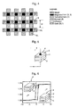
- Such an MTJ layer sequence is shown in FIG. 5: a tunnel barrier layer 1 lies between a soft magnetic layer 2 and a hard magnetic layer 3 and consists of an oxide barrier.
- the tunnel barrier layer 1, the soft magnetic layer 2 and the hard magnetic layer 3 thus form an MTJ layer sequence 4 whose electrical resistance depends on the orientation of the magnetic moments in the two magnetic layers 2 and 3.
- the resistance of the MTJ layer sequence 4 is low, while an antiparallel orientation of these magnetizations results in a higher resistance of the MTJ layer sequence.
- the determination of the cell content of a memory cell formed from such an MTJ layer sequence is measured by passing a current I through the MTJ layer sequence 4. From the height of this stream I It can then be concluded whether the MTJ layer sequence 4 is in a state of high resistance (antiparallel orientation of the magnetizations) or in a state of low resistance (parallel orientation of the magnetizations). Each of these states can then be assigned an information content "0" or "1".
- the abscissa represents the magnetic field generated by corresponding currents in the bit lines and word lines and the ordinate the normalized resistance value. It can clearly be seen that with parallel orientation of the magnetizations, the resistance of the MTJ layer sequence 4 is about 15% lower than in antiparallel orientation.
- the parallel orientation of the magnetization is here associated with the information content "0", while the antiparallel orientation of the magnetization has the information content "1". Of course, other assignments are possible.
- the writing in memory cells consisting of MTJ layer sequences 4 takes place by controlling the orientation of the magnetic moments in a controlled manner.
- the memory cell is placed between two electrical conductors, namely a bit line BL and a word line WL, as shown in FIG.
- suitable currents are sent through these lines BL and WL, a magnetic field can be generated at the location of the MTJ layer sequence 4, ie in the existing memory cell, by which the direction of the magnetic moments, ie in particular the direction of the magnetic moments in the soft magnetic layer 2, can be adjusted.
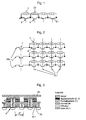
- FIG. 8 shows the already mentioned simplest imaginable structure of an MRAM arrangement: MTJ layer sequences 4, which each form memory cells, are located at the crossing points of parallel word lines WL1, WL2, WL3 and bit lines BL1, BL2.
- a particular memory cell will be described, for example, by sending corresponding currents through bit line BL2 and word line WL3.
- bit line BL2 At the point of intersection of the bit line BL2 with the word line WL3 (ie in the rightmost direction in FIG. 8), a corresponding magnetic field prevails as a result of these currents, so that the MTJ layer sequence lying there or the memory cell formed by it are described accordingly.
- An advantage of the arrangement shown in FIG. 8 is its high-density design: per information content or bit, only an area of 4 F 2 is required in a perfectly ideal manner, where F is the "minimum feature size", ie the smallest possible feature size of the technology used means.
- F is the "minimum feature size", ie the smallest possible feature size of the technology used means.
- a major disadvantage of such a design of an MRAM arrangement is to be regarded as meaning that considerable parasitic currents flow through neighboring cells during read-out as a result of the only slight differences in the resistance value (about 15%, see above), so that such an MRAM arrangement as a whole is only very can be read out slowly.
- each individual one Memory cell consists of an MTJ layer sequence 4 and a selection transistor 5.
- a write-in to a memory cell surrounded by a dashed line 6 takes place by sending corresponding currents through the word line WL2 and the bit line BL2.
- the MTJ layer sequence 4 of this memory cell is programmed in a corresponding manner.
- select lines SL11 and SL13 are driven in such a way that the selection transistors 5 connected to them are all blocked.
- a voltage is applied to a select line SL12 such that the selection transistors 5 connected to this line conduct.
- a read signal is applied to a select line SL22 of the select lines SL21 to SL23.
- a signal indicating the state of the MTJ layer sequence 4 ie an information content "0" or "1" can be obtained at the output of the select line SL22.
- the selection transistors and the MTJ layer sequences of the individual memory cells lie parallel to one another. These memory cells or "primitives" are then assembled into chains, with mutually parallel chains forming a memory matrix.
- the selection of a chain in such a memory matrix can be done by a separate selection transistor. That is, each individual string is assigned a separate select transistor at one end of the string.
- the writing into the MRAM arrangement according to the invention takes place in the usual way by applying to the desired word and bit lines in each case a corresponding signal.
- a chain of the memory matrix is first determined via the separate selection transistors. Then all the transistors of this chain are switched through to the transistor of the memory cell whose cell content is to be read. The transistor of the memory cell to be read thus remains locked. If then a current is sent through the chain of this transistor to be read, so the current flows solely through the MTJ layer sequence of the memory cell to be read and through all the selection transistors of the remaining memory cells of the chain. Thus, the cell content of the memory cell to be read can be determined.
- the MRAM device according to the invention is characterized by a small area requirement: in the chain, if designed appropriately, a memory cell comprising an MTJ layer sequence and a selection transistor lying parallel to it has an effective cell area of 4 F 2 . For this, the separate selection transistor of a chain must be counted, which in turn requires an area of 4 F 2 . This results in an effective cell area for each memory cell of 4 F 2 (N + 1) / N for a chain of N memory cells.
- N 1, ie a chain consisting of only one memory cell, there is an effective cell area of 8 F 2 , which corresponds exactly to the hitherto known solution of a series connection of a selection transistor with an MTJ layer sequence.
- the invention can be used particularly advantageously if the condition N> 1 exists in an MRAM arrangement, which of course applies to all memory cells arranged in memory matrices.
- the hitherto conventional principle of a series connection of an MTJ layer arrangement and a selection transistor is completely omitted, and a novel concept is proposed in which the MTJ layer sequence and the selection transistor in each memory cell lie parallel to one another and are combined into chains ,
- FIGS. 5 to 9 have already been explained at the beginning.
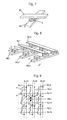
- Fig. 1 shows a chain of an MRAM device according to an embodiment of the present invention with selection transistors 5 and MTJ layer sequences 4, which are each parallel to each other. That is, over the drain-source paths of the selection transistors 5 is in each case an MTJ layer sequence 4, which in turn are connected in series in the chain, as is also true for the drain-source paths of the selection transistors 5.
- FIG. 2 shows an embodiment of the MRAM device according to the invention.
- Fig. 1 shows several of the chains shown in Fig. 1 with MTJ layer sequences 4 and selection transistors 5 parallel to each other, wherein in addition to each chain still a separate selection transistor 7 is connected.
- FIG. 2 also shows first select lines SL1 and row select lines RSL, which are each formed by the separate selection transistors 7 and the drain-source paths of the selection transistors 5.
- a specific memory cell for example a memory cell Z2 of the chain shown in FIG. 1
- the separate selection transistor 7 of this chain is first turned on, while all other separate selection transistors of the memory matrix remain switched off or nonconductive. Then, in this chain, by applying a corresponding signal to the memory cell Z2 associated select line SL1 of the selection transistor 5 of the memory cell Z2 is switched non-conductive, while all other selection transistors 5 of the chain are transferred to the conductive state.
- This is in the chain before a current path I1, as this is indicated in a solid line with arrow schematically in Fig. 1. That is, the resistance state of the MTJ layer sequence of the memory cell Z2 can be easily read out.
- the MTJ layer sequences 4 are located between word lines WL and these perpendicularly crossing bit lines BL. By sending respective currents through the word lines WL and bit lines BL, MTJ layer sequences 4 located at the intersections of such word lines and bit lines can be programmed, as explained above.
- the separate selection transistor 7 of the chain with the memory cell to be read is turned on, while all other separate selection transistors 7 remain blocked. Then, the selection transistor 5 of the memory cell to be read in this chain is blocked or switched off by corresponding activation of the select line SL1, while all other selection transistors of this chain are converted into the conducting state by appropriate control of their gates via the select lines SL1.
- the read current then flows via the row select line RSL, that is to say via the drain-source paths of the selection transistors of the unselected memory cells of the chain and via the MTJ layer sequence 4 selected memory cell with the locked selection transistor 5. In this way, the cell content of the selected memory cell can be read out quickly and without parasitic currents.
- FIGS. 3 and 4 also illustrate the "minimum feature sizes" F of the individual memory cells, each having 2 F.
- the invention thus enables a simply constructed MRAM arrangement, which completely deviates from the previous concept of a series connection of selection transistor and memory cell and instead provides for a parallel connection of selection transistor and MTJ layer sequence.
- a high packing density can be ensured, so that the above object of the invention is achieved in an excellent manner.
- bit lines BL run above the selection transistors 5 and especially above their gate electrodes at a distance from them.
Landscapes
- Engineering & Computer Science (AREA)
- Computer Hardware Design (AREA)
- Mram Or Spin Memory Techniques (AREA)
- Hall/Mr Elements (AREA)
- Semiconductor Memories (AREA)
Applications Claiming Priority (3)
| Application Number | Priority Date | Filing Date | Title |
|---|---|---|---|
| DE10103313A DE10103313A1 (de) | 2001-01-25 | 2001-01-25 | MRAM-Anordnung |
| DE10103313 | 2001-01-25 | ||
| PCT/DE2002/000207 WO2002059898A2 (de) | 2001-01-25 | 2002-01-23 | Mram-anordnung |
Publications (2)
| Publication Number | Publication Date |
|---|---|
| EP1354321A2 EP1354321A2 (de) | 2003-10-22 |
| EP1354321B1 true EP1354321B1 (de) | 2007-05-09 |
Family
ID=7671712
Family Applications (1)
| Application Number | Title | Priority Date | Filing Date |
|---|---|---|---|
| EP02704605A Expired - Lifetime EP1354321B1 (de) | 2001-01-25 | 2002-01-23 | Mram-anordnung |
Country Status (7)
Families Citing this family (33)
| Publication number | Priority date | Publication date | Assignee | Title |
|---|---|---|---|---|
| US6490194B2 (en) * | 2001-01-24 | 2002-12-03 | Infineon Technologies Ag | Serial MRAM device |
| US6911682B2 (en) | 2001-12-28 | 2005-06-28 | Nantero, Inc. | Electromechanical three-trace junction devices |
| US6574130B2 (en) | 2001-07-25 | 2003-06-03 | Nantero, Inc. | Hybrid circuit having nanotube electromechanical memory |
| US7259410B2 (en) | 2001-07-25 | 2007-08-21 | Nantero, Inc. | Devices having horizontally-disposed nanofabric articles and methods of making the same |
| US7566478B2 (en) | 2001-07-25 | 2009-07-28 | Nantero, Inc. | Methods of making carbon nanotube films, layers, fabrics, ribbons, elements and articles |
| US6706402B2 (en) | 2001-07-25 | 2004-03-16 | Nantero, Inc. | Nanotube films and articles |
| US6835591B2 (en) | 2001-07-25 | 2004-12-28 | Nantero, Inc. | Methods of nanotube films and articles |
| US6643165B2 (en) | 2001-07-25 | 2003-11-04 | Nantero, Inc. | Electromechanical memory having cell selection circuitry constructed with nanotube technology |
| US6924538B2 (en) | 2001-07-25 | 2005-08-02 | Nantero, Inc. | Devices having vertically-disposed nanofabric articles and methods of making the same |
| US6919592B2 (en) | 2001-07-25 | 2005-07-19 | Nantero, Inc. | Electromechanical memory array using nanotube ribbons and method for making same |
| DE10149737A1 (de) * | 2001-10-09 | 2003-04-24 | Infineon Technologies Ag | Halbleiterspeicher mit sich kreuzenden Wort- und Bitleitungen, an denen magnetoresistive Speicherzellen angeordnet sind |
| US7176505B2 (en) | 2001-12-28 | 2007-02-13 | Nantero, Inc. | Electromechanical three-trace junction devices |
| US6784028B2 (en) | 2001-12-28 | 2004-08-31 | Nantero, Inc. | Methods of making electromechanical three-trace junction devices |
| US7335395B2 (en) | 2002-04-23 | 2008-02-26 | Nantero, Inc. | Methods of using pre-formed nanotubes to make carbon nanotube films, layers, fabrics, ribbons, elements and articles |
| KR20030089078A (ko) * | 2002-05-16 | 2003-11-21 | 주식회사 하이닉스반도체 | 자기터널접합소자를 갖는 자기메모리셀 |
| US6791867B2 (en) * | 2002-11-18 | 2004-09-14 | Hewlett-Packard Development Company, L.P. | Selection of memory cells in data storage devices |
| US7560136B2 (en) | 2003-01-13 | 2009-07-14 | Nantero, Inc. | Methods of using thin metal layers to make carbon nanotube films, layers, fabrics, ribbons, elements and articles |
| JP4415745B2 (ja) * | 2004-04-22 | 2010-02-17 | ソニー株式会社 | 固体メモリ装置 |
| DE102004026003B3 (de) * | 2004-05-27 | 2006-01-19 | Infineon Technologies Ag | Resistive Speicherzellen-Anordnung |
| EP1768187B1 (en) * | 2005-09-26 | 2008-03-26 | Qimonda AG | Microelectronic device with storage elements and method of producing the same |
| US7423281B2 (en) * | 2005-09-26 | 2008-09-09 | Infineon Technologies Ag | Microelectronic device with a plurality of storage elements in serial connection and method of producing the same |
| US7362644B2 (en) * | 2005-12-20 | 2008-04-22 | Magic Technologies, Inc. | Configurable MRAM and method of configuration |
| JP2008159612A (ja) | 2006-12-20 | 2008-07-10 | Toshiba Corp | 半導体記憶装置 |
| US8211557B2 (en) * | 2007-01-31 | 2012-07-03 | Carnegie Mellon University | Binary anisotropy media |
| JP2008251059A (ja) * | 2007-03-29 | 2008-10-16 | Toshiba Corp | 不揮発性半導体記憶装置およびそのデータ消去方法 |
| US7826258B2 (en) * | 2008-03-24 | 2010-11-02 | Carnegie Mellon University | Crossbar diode-switched magnetoresistive random access memory system |
| JP2012234884A (ja) * | 2011-04-28 | 2012-11-29 | Toshiba Corp | 磁気ランダムアクセスメモリ及びその製造方法 |
| JP2013026337A (ja) | 2011-07-19 | 2013-02-04 | Renesas Electronics Corp | 半導体装置及び磁気ランダムアクセスメモリ |
| US8995180B2 (en) * | 2012-11-29 | 2015-03-31 | Taiwan Semiconductor Manufacturing Company, Ltd. | Magnetoresistive random access memory (MRAM) differential bit cell and method of use |
| US9653137B2 (en) * | 2015-04-10 | 2017-05-16 | Globalfoundries Singapore Pte. Ltd. | STT-MRAM bitcell for embedded flash applications |
| US9647037B2 (en) | 2015-08-25 | 2017-05-09 | Qualcomm Incorporated | Resistive random access memory device with resistance-based storage element and method of fabricating same |
| US10630296B2 (en) * | 2017-09-12 | 2020-04-21 | iCometrue Company Ltd. | Logic drive with brain-like elasticity and integrality based on standard commodity FPGA IC chips using non-volatile memory cells |
| CN115917648A (zh) * | 2020-08-31 | 2023-04-04 | 华为技术有限公司 | 一种存储器 |
Citations (3)
| Publication number | Priority date | Publication date | Assignee | Title |
|---|---|---|---|---|
| EP1316091A2 (en) * | 2000-08-28 | 2003-06-04 | Motorola, Inc. | Mtj mram parallel-parallel architecture |
| EP1356469A2 (en) * | 2000-08-28 | 2003-10-29 | Motorola, Inc. | Mtj mram series-parallel architecture |
| EP1358679A2 (en) * | 2001-01-24 | 2003-11-05 | Infineon Technologies North America Corp. | Serial mram device |
Family Cites Families (7)
| Publication number | Priority date | Publication date | Assignee | Title |
|---|---|---|---|---|
| US5734605A (en) * | 1996-09-10 | 1998-03-31 | Motorola, Inc. | Multi-layer magnetic tunneling junction memory cells |
| US5894447A (en) * | 1996-09-26 | 1999-04-13 | Kabushiki Kaisha Toshiba | Semiconductor memory device including a particular memory cell block structure |
| US5940319A (en) * | 1998-08-31 | 1999-08-17 | Motorola, Inc. | Magnetic random access memory and fabricating method thereof |
| JP2000132961A (ja) * | 1998-10-23 | 2000-05-12 | Canon Inc | 磁気薄膜メモリ、磁気薄膜メモリの読出し方法、及び磁気薄膜メモリの書込み方法 |
| US6153443A (en) * | 1998-12-21 | 2000-11-28 | Motorola, Inc. | Method of fabricating a magnetic random access memory |
| US6165803A (en) * | 1999-05-17 | 2000-12-26 | Motorola, Inc. | Magnetic random access memory and fabricating method thereof |
| US6512690B1 (en) * | 2001-08-15 | 2003-01-28 | Read-Rite Corporation | High sensitivity common source amplifier MRAM cell, memory array and read/write scheme |
-
2001
- 2001-01-25 DE DE10103313A patent/DE10103313A1/de not_active Ceased
-
2002
- 2002-01-23 EP EP02704605A patent/EP1354321B1/de not_active Expired - Lifetime
- 2002-01-23 DE DE50210116T patent/DE50210116D1/de not_active Expired - Fee Related
- 2002-01-23 JP JP2002560137A patent/JP2004517504A/ja active Pending
- 2002-01-23 KR KR10-2003-7009798A patent/KR20030072605A/ko not_active Ceased
- 2002-01-23 CN CNB028041763A patent/CN100365734C/zh not_active Expired - Fee Related
- 2002-01-23 WO PCT/DE2002/000207 patent/WO2002059898A2/de active IP Right Grant
-
2003
- 2003-07-25 US US10/627,904 patent/US6791871B2/en not_active Expired - Fee Related
Patent Citations (3)
| Publication number | Priority date | Publication date | Assignee | Title |
|---|---|---|---|---|
| EP1316091A2 (en) * | 2000-08-28 | 2003-06-04 | Motorola, Inc. | Mtj mram parallel-parallel architecture |
| EP1356469A2 (en) * | 2000-08-28 | 2003-10-29 | Motorola, Inc. | Mtj mram series-parallel architecture |
| EP1358679A2 (en) * | 2001-01-24 | 2003-11-05 | Infineon Technologies North America Corp. | Serial mram device |
Also Published As
| Publication number | Publication date |
|---|---|
| WO2002059898A2 (de) | 2002-08-01 |
| JP2004517504A (ja) | 2004-06-10 |
| DE10103313A1 (de) | 2002-08-22 |
| CN1489767A (zh) | 2004-04-14 |
| US20040017706A1 (en) | 2004-01-29 |
| US6791871B2 (en) | 2004-09-14 |
| CN100365734C (zh) | 2008-01-30 |
| DE50210116D1 (de) | 2007-06-21 |
| EP1354321A2 (de) | 2003-10-22 |
| KR20030072605A (ko) | 2003-09-15 |
| WO2002059898A3 (de) | 2002-09-26 |
Similar Documents
| Publication | Publication Date | Title |
|---|---|---|
| EP1354321B1 (de) | Mram-anordnung | |
| DE10041378C1 (de) | MRAM-Anordnung | |
| DE102005046426B4 (de) | MRAM und Verfahren zu dessen Herstellung | |
| DE112010003400B4 (de) | Speicherarchitektur und Verwendung eines magnetischen Racetrack-Speichers | |
| EP1141960B1 (de) | Schreib-/lesearchitektur für mram | |
| DE102005035166B4 (de) | Magnetisches Speicherelement mit magnetischer Durchführung und magnetischem Sensorelement sowie magnetischem Direktzugriffsspeicher | |
| DE10032271C2 (de) | MRAM-Anordnung | |
| DE10314812A1 (de) | Magnetische Kleinbereichs-Speichervorrichtungen | |
| DE10235424A1 (de) | Magnetische Dünnfilm-Speichervorrichtung mit Speicherzellen mit einem magnetischen Tunnelübergang | |
| DE112012004304B4 (de) | Magnetoresistiver Direktzugriffsspeicher mit Mehrbit-Spinmomenttransfer mit einem einzelnen Stapel von Magnettunnelübergängen | |
| DE60311954T2 (de) | Magnetischer Direktzugriffspeicher zur Speicherung von Informationen unter Verwendung des Magnetoresistiveffekts | |
| DE60307459T2 (de) | Mram-zelle und speicherarchitektur mit maximalem lesesignal und reduzierter elektromagnetischer interferenz | |
| DE19823826A1 (de) | MRAM-Speicher sowie Verfahren zum Lesen/Schreiben digitaler Information in einen derartigen Speicher | |
| DE102005046425A1 (de) | Array resistiver Speicherzellen und Verfahren zum Erfassen von Widerstandswerten solcher Zellen | |
| EP1202283B1 (de) | MRAM-Anordnung | |
| EP1174924A2 (de) | MRAM-Speicherzelle | |
| DE10032272C2 (de) | Strom-Treiberanordnung für MRAM | |
| DE102008045542A1 (de) | Integrierter Schaltkreis, Zellenanordnung, Verfahren zum Betreiben eines integrierten Schaltkreises, Speichermodul | |
| DE10342359A1 (de) | MRAM mit zwei Schreibleitern | |
| DE10056830C2 (de) | Integrierte magnetoresistive Halbleiterspeicheranordnung | |
| DE102005046777B4 (de) | Halbleiterspeicher-Einrichtung | |
| WO2002084705A2 (de) | Verfahren zum betrieb einer mram-halbleiterspeicheranordnung | |
| DE102005035164A1 (de) | MRAM mit vertikalem Speicherelement und Feldsensor | |
| DE1524886A1 (de) | Assoziativspeicher mit Duennschichtelementen | |
| DE10033486A1 (de) | Integrierter Speicher mit Speicherzellen mit magnetoresistivem Speichereffekt |
Legal Events
| Date | Code | Title | Description |
|---|---|---|---|
| PUAI | Public reference made under article 153(3) epc to a published international application that has entered the european phase |
Free format text: ORIGINAL CODE: 0009012 |
|
| 17P | Request for examination filed |
Effective date: 20030708 |
|
| AK | Designated contracting states |
Kind code of ref document: A2 Designated state(s): DE FR GB IE IT |
|
| AX | Request for extension of the european patent |
Extension state: AL LT LV MK RO SI |
|
| 17Q | First examination report despatched |
Effective date: 20040129 |
|
| GRAP | Despatch of communication of intention to grant a patent |
Free format text: ORIGINAL CODE: EPIDOSNIGR1 |
|
| GRAS | Grant fee paid |
Free format text: ORIGINAL CODE: EPIDOSNIGR3 |
|
| GRAA | (expected) grant |
Free format text: ORIGINAL CODE: 0009210 |
|
| AK | Designated contracting states |
Kind code of ref document: B1 Designated state(s): DE FR GB IE IT |
|
| REG | Reference to a national code |
Ref country code: GB Ref legal event code: FG4D Free format text: NOT ENGLISH |
|
| REG | Reference to a national code |
Ref country code: IE Ref legal event code: FG4D Free format text: LANGUAGE OF EP DOCUMENT: GERMAN |
|
| REF | Corresponds to: |
Ref document number: 50210116 Country of ref document: DE Date of ref document: 20070621 Kind code of ref document: P |
|
| GBV | Gb: ep patent (uk) treated as always having been void in accordance with gb section 77(7)/1977 [no translation filed] |
Effective date: 20070509 |
|
| REG | Reference to a national code |
Ref country code: IE Ref legal event code: FD4D |
|
| EN | Fr: translation not filed | ||
| PG25 | Lapsed in a contracting state [announced via postgrant information from national office to epo] |
Ref country code: IE Free format text: LAPSE BECAUSE OF FAILURE TO SUBMIT A TRANSLATION OF THE DESCRIPTION OR TO PAY THE FEE WITHIN THE PRESCRIBED TIME-LIMIT Effective date: 20070509 |
|
| PLBE | No opposition filed within time limit |
Free format text: ORIGINAL CODE: 0009261 |
|
| STAA | Information on the status of an ep patent application or granted ep patent |
Free format text: STATUS: NO OPPOSITION FILED WITHIN TIME LIMIT |
|
| 26N | No opposition filed |
Effective date: 20080212 |
|
| PG25 | Lapsed in a contracting state [announced via postgrant information from national office to epo] |
Ref country code: GB Free format text: LAPSE BECAUSE OF FAILURE TO SUBMIT A TRANSLATION OF THE DESCRIPTION OR TO PAY THE FEE WITHIN THE PRESCRIBED TIME-LIMIT Effective date: 20070509 Ref country code: IT Free format text: LAPSE BECAUSE OF FAILURE TO SUBMIT A TRANSLATION OF THE DESCRIPTION OR TO PAY THE FEE WITHIN THE PRESCRIBED TIME-LIMIT Effective date: 20070509 |
|
| PG25 | Lapsed in a contracting state [announced via postgrant information from national office to epo] |
Ref country code: FR Free format text: LAPSE BECAUSE OF FAILURE TO SUBMIT A TRANSLATION OF THE DESCRIPTION OR TO PAY THE FEE WITHIN THE PRESCRIBED TIME-LIMIT Effective date: 20080104 |
|
| PGFP | Annual fee paid to national office [announced via postgrant information from national office to epo] |
Ref country code: DE Payment date: 20080315 Year of fee payment: 7 |
|
| PG25 | Lapsed in a contracting state [announced via postgrant information from national office to epo] |
Ref country code: DE Free format text: LAPSE BECAUSE OF NON-PAYMENT OF DUE FEES Effective date: 20090801 |