EP1349138A2 - Elektrolumineszenzanzeigevorrichtung und Ansteuerungsverfahren dafür - Google Patents
Elektrolumineszenzanzeigevorrichtung und Ansteuerungsverfahren dafür Download PDFInfo
- Publication number
- EP1349138A2 EP1349138A2 EP03006078A EP03006078A EP1349138A2 EP 1349138 A2 EP1349138 A2 EP 1349138A2 EP 03006078 A EP03006078 A EP 03006078A EP 03006078 A EP03006078 A EP 03006078A EP 1349138 A2 EP1349138 A2 EP 1349138A2
- Authority
- EP
- European Patent Office
- Prior art keywords
- electrodes
- organic
- row direction
- direction electrodes
- column
- Prior art date
- Legal status (The legal status is an assumption and is not a legal conclusion. Google has not performed a legal analysis and makes no representation as to the accuracy of the status listed.)
- Withdrawn
Links
Images


Classifications
-
- G—PHYSICS
- G09—EDUCATION; CRYPTOGRAPHY; DISPLAY; ADVERTISING; SEALS
- G09G—ARRANGEMENTS OR CIRCUITS FOR CONTROL OF INDICATING DEVICES USING STATIC MEANS TO PRESENT VARIABLE INFORMATION
- G09G3/00—Control arrangements or circuits, of interest only in connection with visual indicators other than cathode-ray tubes
- G09G3/20—Control arrangements or circuits, of interest only in connection with visual indicators other than cathode-ray tubes for presentation of an assembly of a number of characters, e.g. a page, by composing the assembly by combination of individual elements arranged in a matrix no fixed position being assigned to or needed to be assigned to the individual characters or partial characters
- G09G3/22—Control arrangements or circuits, of interest only in connection with visual indicators other than cathode-ray tubes for presentation of an assembly of a number of characters, e.g. a page, by composing the assembly by combination of individual elements arranged in a matrix no fixed position being assigned to or needed to be assigned to the individual characters or partial characters using controlled light sources
- G09G3/30—Control arrangements or circuits, of interest only in connection with visual indicators other than cathode-ray tubes for presentation of an assembly of a number of characters, e.g. a page, by composing the assembly by combination of individual elements arranged in a matrix no fixed position being assigned to or needed to be assigned to the individual characters or partial characters using controlled light sources using electroluminescent panels
- G09G3/32—Control arrangements or circuits, of interest only in connection with visual indicators other than cathode-ray tubes for presentation of an assembly of a number of characters, e.g. a page, by composing the assembly by combination of individual elements arranged in a matrix no fixed position being assigned to or needed to be assigned to the individual characters or partial characters using controlled light sources using electroluminescent panels semiconductive, e.g. using light-emitting diodes [LED]
- G09G3/3208—Control arrangements or circuits, of interest only in connection with visual indicators other than cathode-ray tubes for presentation of an assembly of a number of characters, e.g. a page, by composing the assembly by combination of individual elements arranged in a matrix no fixed position being assigned to or needed to be assigned to the individual characters or partial characters using controlled light sources using electroluminescent panels semiconductive, e.g. using light-emitting diodes [LED] organic, e.g. using organic light-emitting diodes [OLED]
- G09G3/3216—Control arrangements or circuits, of interest only in connection with visual indicators other than cathode-ray tubes for presentation of an assembly of a number of characters, e.g. a page, by composing the assembly by combination of individual elements arranged in a matrix no fixed position being assigned to or needed to be assigned to the individual characters or partial characters using controlled light sources using electroluminescent panels semiconductive, e.g. using light-emitting diodes [LED] organic, e.g. using organic light-emitting diodes [OLED] using a passive matrix
-
- G—PHYSICS
- G09—EDUCATION; CRYPTOGRAPHY; DISPLAY; ADVERTISING; SEALS
- G09G—ARRANGEMENTS OR CIRCUITS FOR CONTROL OF INDICATING DEVICES USING STATIC MEANS TO PRESENT VARIABLE INFORMATION
- G09G3/00—Control arrangements or circuits, of interest only in connection with visual indicators other than cathode-ray tubes
- G09G3/20—Control arrangements or circuits, of interest only in connection with visual indicators other than cathode-ray tubes for presentation of an assembly of a number of characters, e.g. a page, by composing the assembly by combination of individual elements arranged in a matrix no fixed position being assigned to or needed to be assigned to the individual characters or partial characters
- G09G3/22—Control arrangements or circuits, of interest only in connection with visual indicators other than cathode-ray tubes for presentation of an assembly of a number of characters, e.g. a page, by composing the assembly by combination of individual elements arranged in a matrix no fixed position being assigned to or needed to be assigned to the individual characters or partial characters using controlled light sources
- G09G3/30—Control arrangements or circuits, of interest only in connection with visual indicators other than cathode-ray tubes for presentation of an assembly of a number of characters, e.g. a page, by composing the assembly by combination of individual elements arranged in a matrix no fixed position being assigned to or needed to be assigned to the individual characters or partial characters using controlled light sources using electroluminescent panels
- G09G3/32—Control arrangements or circuits, of interest only in connection with visual indicators other than cathode-ray tubes for presentation of an assembly of a number of characters, e.g. a page, by composing the assembly by combination of individual elements arranged in a matrix no fixed position being assigned to or needed to be assigned to the individual characters or partial characters using controlled light sources using electroluminescent panels semiconductive, e.g. using light-emitting diodes [LED]
- G09G3/3208—Control arrangements or circuits, of interest only in connection with visual indicators other than cathode-ray tubes for presentation of an assembly of a number of characters, e.g. a page, by composing the assembly by combination of individual elements arranged in a matrix no fixed position being assigned to or needed to be assigned to the individual characters or partial characters using controlled light sources using electroluminescent panels semiconductive, e.g. using light-emitting diodes [LED] organic, e.g. using organic light-emitting diodes [OLED]
-
- G—PHYSICS
- G09—EDUCATION; CRYPTOGRAPHY; DISPLAY; ADVERTISING; SEALS
- G09G—ARRANGEMENTS OR CIRCUITS FOR CONTROL OF INDICATING DEVICES USING STATIC MEANS TO PRESENT VARIABLE INFORMATION
- G09G2300/00—Aspects of the constitution of display devices
- G09G2300/04—Structural and physical details of display devices
- G09G2300/0421—Structural details of the set of electrodes
- G09G2300/0426—Layout of electrodes and connections
-
- G—PHYSICS
- G09—EDUCATION; CRYPTOGRAPHY; DISPLAY; ADVERTISING; SEALS
- G09G—ARRANGEMENTS OR CIRCUITS FOR CONTROL OF INDICATING DEVICES USING STATIC MEANS TO PRESENT VARIABLE INFORMATION
- G09G2300/00—Aspects of the constitution of display devices
- G09G2300/04—Structural and physical details of display devices
- G09G2300/0439—Pixel structures
-
- G—PHYSICS
- G09—EDUCATION; CRYPTOGRAPHY; DISPLAY; ADVERTISING; SEALS
- G09G—ARRANGEMENTS OR CIRCUITS FOR CONTROL OF INDICATING DEVICES USING STATIC MEANS TO PRESENT VARIABLE INFORMATION
- G09G2310/00—Command of the display device
- G09G2310/02—Addressing, scanning or driving the display screen or processing steps related thereto
- G09G2310/0202—Addressing of scan or signal lines
- G09G2310/0205—Simultaneous scanning of several lines in flat panels
-
- G—PHYSICS
- G09—EDUCATION; CRYPTOGRAPHY; DISPLAY; ADVERTISING; SEALS
- G09G—ARRANGEMENTS OR CIRCUITS FOR CONTROL OF INDICATING DEVICES USING STATIC MEANS TO PRESENT VARIABLE INFORMATION
- G09G2310/00—Command of the display device
- G09G2310/02—Addressing, scanning or driving the display screen or processing steps related thereto
- G09G2310/0202—Addressing of scan or signal lines
- G09G2310/0221—Addressing of scan or signal lines with use of split matrices
-
- G—PHYSICS
- G09—EDUCATION; CRYPTOGRAPHY; DISPLAY; ADVERTISING; SEALS
- G09G—ARRANGEMENTS OR CIRCUITS FOR CONTROL OF INDICATING DEVICES USING STATIC MEANS TO PRESENT VARIABLE INFORMATION
- G09G2310/00—Command of the display device
- G09G2310/04—Partial updating of the display screen
Definitions
- the present invention relates to a driving method and a driving apparatus for a display panel using an organic EL element. More particularly, in an organic EL matrix panel based on the multiple line driving method, a driving method is achieved which is capable of obtaining sufficient luminance necessary for the matrix panel and which improves the reliability of an organic EL element, without applying an excessive voltage for high duty drive to the organic EL element that forms pixels.
- the organic EL elements are now being commercialized as information displays having characteristics such as spontaneous light, high luminance, high efficiency and light weight mainly in compact panels and portable information terminals.
- Displaying types for the displays are generally classified into the following types: an active matrix type having an active device such as, for example, an FET and a charge storage capacitor for each pixel, and a passive type having a plurality of electrodes that expand simply in row and column directions, and for forming an image by selecting intersection points thereof to emit light.
- the FET circuit and the charge storage capacitor are disposed at a positive pole of each pixel, and a voltage applied to each pixel by the stored charge of the capacitor is maintained for a certain period of time.
- the active matrix type has a system in which each pixel is selected once in one frame of a screen display while luminance information to be displayed is sent thereto, and the same voltage is applied to the organic EL element constituting the pixels constantly during one frame, thereby performing each display. Therefore, in the active matrix type, 100% duty drive is possible.
- the FET circuit constituted of, for example, a TFT, and the capacitor must both be formed on the same substrate, together with each organic EL element.
- the passive type a plurality of anode electrodes and a plurality of cathode electrodes are formed into strips via an organic EL thin film, in such a way that they cross each other at right angles, thereby preparing a matrix structure in which the luminescence of the organic EL thin film is controlled by the row electrodes and column electrodes at orthogonal points. Since the response speed of an organic EL element is usually 1 ⁇ s or less, scanning display due to this matrix structure is possible.
- the advantage of the passive type is that production costs can be reduced since the configuration of the element is simple and the accuracy of processing is not required as severely as in the active matrix type.
- the organic EL thin film element has rectification properties that can adequately suppress crosstalk caused by a current flowing in the opposite direction, and has such characteristics that a high-capacity panel can be driven with a simple drive waveform. For this reason, most of the organic EL element panels in present use utilize the passive type.
- FIG. 1 schematically shows a conventional passive type display panel and its control circuit.
- a display panel 1 a plurality of strip-shaped anodes 3 made of a transparent electrode material such as indium tin oxide (ITO) are formed in parallel with each other on the surface of a transparent substrate 2.
- An organic light emitting layer 4 is formed covering the plurality of anodes 3, and on its upper surface, a plurality of strip-shaped cathodes 5 constituted of a metallic thin film are formed in parallel with each other.
- the anodes 3 and cathodes 5 are usually formed to cross each other at right angles, and the organic light emitting layer at each intersection 6 forms a pixel.
- Each of the strip-shaped anodes 3 are connected to a data electrode driving portion 7, and each of the strip-shaped cathodes 5 is connected to a scanning electrode driving portion 8.
- the data electrode driving portion 7 and scanning electrode driving portion 8 are controlled by a display control portion 9, and the display control portion 9 is controlled by a main control portion 13 for receiving a video signal 30 and controlling the operation of the entire panel.
- Light emission processing for one frame period of the display panel is performed in such a way that the scanning electrode driving portion 8 first sequentially selects each cathode 5 in 1 to N (rows) so as to enable each row to be conductive.
- the luminance of each pixel belonging to each selected row is controlled by the data electrode driving portion 7 by corresponding conduction state of each corresponding row with the signal strength of the video signal 30 by means of 1 to M (columns) of the anodes 3.
- each organic EL element needs to emit light with a luminance N times as high as the luminance to be actually displayed.
- one object of this invention is to accomplish a driving method which, in the driving of the organic EL matrix panel based on a multiple line driving method, enables the matrix panel to have a sufficient luminance, without driving the organic EL element in accordance with an inappropriate duty ratio, which improves the reliability of the organic EL element.
- a driving method for a matrix type organic EL element which has a plurality of row direction electrodes and a plurality of column direction electrodes arranged via an organic light emitting layer and which is capable of displaying a predetermined image, the method comprising:
- the driving method for the organic EL element comprises the steps of:
- the driving method for the organic EL element can be provided which comprises the step of:
- the present invention can provide a matrix type organic EL apparatus which has a plurality of row direction electrodes and a plurality of column direction electrodes arranged via an organic light emitting layer and which is capable of displaying a predetermined image, and the apparatus has:
- the organic EL apparatus can be provided in which the two or more adjacent rows of the plurality of row direction electrodes are integrally formed as one set of row direction electrodes, and the organic EL apparatus can be provided in which low-resistance wiring electrodes are provided as auxiliary electrodes connected to each display portion of the column direction electrodes.
- FIG. 2 shows a basic configuration of an organic electroluminescence element display based on a double line driving method according to the present invention.
- This display is a matrix type organic electroluminescence element capable of displaying various gradations, colors and optional shapes, for example. Color specification does not particularly limits the present invention, and known methods can be applied as the color specification of the normal organic electroluminescence element.
- the display is divided into two upper and lower portions.
- 10 1 , 10 2 , 10 3 , ..., 10 N-1 , 10 N on the left side are no. 1, 2, 3 ..., N-1, N row wires in the display and used in common in the divided two upper and lower portions.
- Horizontally extending electrodes 11 1 , 11 2 , 11 3, ..., 11 N respectively connected to the above row wires are a first set of no. 1, 2, 3 ..., N (upper) row electrodes
- 12 1 , 12 2 , 12 3 , ..., 12 N are a second set of no. 1, 2, 3 ..., N (lower) row electrodes.
- Vertically extending electrodes 21 1 , 21 2 , 21 3 , 21 4 , ..., 21 M are a first set of no. 1, 2, 3, 4 ..., M (upper) column electrodes, and 22 1 , 22 2 , 22 3 , 22 4 , ..., 22 M are a second set of no. 1, 2, 3, 4 ..., M (lower) column electrodes.
- a control signal for row scanning is sequentially applied to the common row wires 10 1 , 10 2 , 10 3 , ..., 10 N-1 , 10 N on a time division basis totally without reference to a signal image.
- signal voltage patterns corresponding to each luminance to be displayed in the row presently targeted for scanning are applied respectively at the same time to column wires (not shown) connected to the electrode columns 21 1 , 21 2 , 21 3 , 21 4 , ..., 21 M and the electrode columns 22 1 , 22 2 , 22 3 , 22 4 , ..., 22 M respectively.
- FIG. 3 shows the relation of luminance to a voltage applied to the organic electroluminescence element.
- FIG. 4 shows one example of the time-related change of one portion of the control voltage applied to the organic electroluminescence element panel, when it emits light with a certain degree of luminance.
- (a) indicates the time-related change of a voltage V211, which is a luminance signal voltage applied to the row electrode 21 1 .
- (b 1 ), (b 2 )...(b N ) indicate the time-related change of voltages V11 1 , V11 2 , ..., V11 N respectively applied to the row electrodes 11 1 , 11 2, ..., 11 N on a scanned side.
- (c) indicates the time-related change of a voltage V EL applied to the organic electroluminescence element in the portion of the intersection 31.
- Successive selection of the row electrodes 11 1 , 11 2 , 11 3 , 11 4 , ..., 11 N for one frame period are performed by sequentially changing the voltage applied to the row electrodes from +V to 0, and then returning it from 0 to +V after each selection period.
- Signals are applied to the column electrodes with 0V in a pixel region where light is not emitted and +V in a pixel region where light is emitted, thereby enabling light emission with a certain degree of luminance in a predetermined pixel region on a horizontal scanning line of the display.
- Timing numbers 1, 2...N are indicated at the top.
- the voltage +V is applied to the V21 1 , and the voltage 0 to the V11 1 .
- the voltage applied to the V11 2 to V11 N that are not scanned apart from the V11 1 is +V.
- the voltage +V is applied as V EL to the selected intersection 31 of FIG. 2 as indicated by (c), and thus the region of this selected intersection 31 emits light.
- +V is applied to the other row electrodes 11 2 , 11 3 , 11 4 , ..., 11 N , and 0V biases between the row electrodes 11 2 , 11 3 , 11 4 , ..., 11 N and the column electrode V21 1 , so that these areas will be in a nonluminous state.
- each intersection of the row electrode 11 2 and the column electrodes 21 1 , 21 2 , 21 3 , 21 4 , ..., 21M generally emits light or is in the nonluminous state, in connection with the signal voltage applied to the voltages V21 1 , V21 2 , ..., V21 M , which are applied to the column electrodes 21 1 , 31 3 , 21 3 , 21 4 , ..., 21 M .
- 0V is applied to the column electrode 211 selected at the timing 1. This causes the V EL at the intersection 31 to be -V, leading the intersection 31 into the nonluminous state. Even if +V were applied to the column electrode 21 1 at the timing 2, the V EL would be 0V (not shown), and the intersection 31 in an unselected state would be in the nonluminous state.
- the intersection will be in a luminous state when the voltage applied to the organic electroluminescence element is +Vn, and in a nonluminous state when the voltage is 0 or -V, thereby enabling the matrix panel to be driven. Therefore, when a desired luminance is to be obtained by means of the voltage applied to each organic electroluminescence element, the relationship between the voltage applied to each organic electroluminescence element and the luminance is important. In general, in the organic electroluminescence element with favorable characteristics, its luminance is essentially proportionate to a current flowing in its organic electroluminescence element portion in a broad range.
- the column electrodes 21 1 , 21 2 , 21 3 , 21 4 , ..., 21 M of the actual luminous panel are desirably driven selectively by a current driving power source by which currents are controlled in response to the amplitude of a video signal 30, respectively.
- the display panel of FIG. 2 here comprises the basically equivalent upper and lower two display portions 14 and 15, the same scanning signal is applied at the same timing to the wires of pairs of the row wires 11 1 and 121, 11 2 and 12 2 , 11 3 and 12 3 , ..., 11 N and 12 N .
- a data signal corresponding to the luminance of the display portions is applied to the column wires 21 1 , 21 2 , 21 3 , 21 4 , ..., 21 M , and 22 1 , 22 2 , 22 3 , 22 4 , ..., 22 M , thereby allowing information display, that is, image display corresponding to each portion at each timing.
- an indium tin oxide (ITO) electrode or an indium zinc oxide (IZO) electrode which are generally high-resistance anode materials as compared with electrode materials generally used, is used as a wiring material for the column electrodes 21 1 , 21 2 , 21 3 , 21 4 , ..., 21 M and 22 1 , 22 2 , 22 3 , 22 4 , ..., 22 M in the upper portion 14 and lower portion 15 in the drawing, such an advantage is obtained that the resistance of the column electrodes can be substantially reduced, since the length of each electrode is half. Thus, a voltage drop due to serial resistance effects is reduced in each element, so that response time can be shortened.
- ITO indium tin oxide
- IZO indium zinc oxide
- the electrode (cathode 5) after the organic material is formed is formed by a method such as deposition, in association with chemical resistance and adhesion properties of an organic material 4. Therefore, in the most convenient method that can keep the electrode shape of FIG. 2 unchanged, although this is not an exclusive method, it is desirable that, after an anode such as ITO to be the column electrode in which patters are formed in advance is produced, an organic thin film is formed by deposition, and finally the electrode 5 to be the common row electrode is formed by such a method as mask deposition.
- FIG. 5 schematically shows the display panel and its control circuit in the embodiment of FIG. 2.
- the main difference from the conventional display panel and its control circuit shown in FIG. 1 is in that the display panel is formed with a plurality of equivalent display portions 14 and 15, as described above.
- the row electrode (not shown) of each display portion is driven by a scanning electrode diving portion 8 common to the display portions, but the point is that the column electrodes (not shown) are driven by each of the data electrode driving portions 16 and 17 that are separately provided in each display portion.
- the continuous data signal 30 constituting one frame is sequentially divided into a plurality of continuous data signals in accordance with the number of display portions 14 and 15. Each divided signal portion is once stored in a signal data storage portion 18. Each corresponding piece of data is sent to each of the electrode driving portions 16 and 17, and by controlling each corresponding pixel to emit light at the same time in each of the display portions 15 and 16 synchronously with the signal of the common scanning electrode driving portion, an image is reproduced as one entire display panel image.
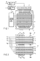
- FIG. 6, FIG. 7 and FIG. 8 show a concrete example of the row and column electrodes in an alternative embodiment.
- FIG. 6 shows the arrangement of the electrodes in accordance with the double line driving method in the alternative embodiment
- 11 1 , 11 2 , 11 3 , ..., 11 N indicate a set of no. 1, 2, 3, ..., N row electrodes
- 21 1 , 21 2 , 21 3 , 21 4 , ..., 21 M indicate a first set of no. 1, 2, 3, 4 ..., M column electrodes.
- 12 1 , 12 2 , 12 3 , ..., 12 N indicate a second set of no. 1, 2, 3 ..., N row electrodes
- 22 1 , 22 2 , 22 3 , 22 4 , ..., 22 M indicate a second set of no. 1, 2, 3, 4 ..., M column electrodes.
- FIG. 7 here shows an example of a row electrode arrangement, and 111, 11 2 , ..., 11 N respectively indicate no. 1, 2, 3, ..., N row electrodes.
- FIG. 8 shows the constitution of column electrodes, and 21 1 , 21 2 , 21 3 , 21 4 , ..., 21 M indicate a first set of column electrodes, and 22 1 , 22 2 , 22 3 , 22 4 , ..., 22 M indicate a second set of column electrodes.
- FIG. 6 shows the first set of column electrodes 21 1 , 21 2 , 21 3 , 21 4 , .... 21 M and the second set of column electrodes 22 1 , 22 2 , 22 3 , 22 4 , ..., 22 M of FIG. 8 that are disposed via an organic luminous film (not shown) on the row electrodes 11 1 , 11 2 , ...11 N of FIG. 7.
- a crossing electrode constitution given only as an example of a convenient constitution, would be built by such a form that two row scanning electrodes are commonly driven, and a voltage is independently applied to each of the upper and lower column signal electrodes.
- second electrode regions 19 and 20 from the top of the column electrodes 21 1 and 221 are formed as adjacent electrode regions 23 and 24 on the same second electrode 11 2 from the top in the case of FIG. 6, and then a simultaneous luminance data signal is applied, thus controlling light emission, as in FIG. 2.
- FIG. 9 shows a further alternative embodiment, and an example of an arrangement where the column electrodes are constituted with a combination of an electrode 25 of a light emitting portion and an auxiliary wire 26 made of a low-resistance metallic material such as gold.
- 21 1 , 21 2 , 21 3 , 21 4 , ..., 21M are the first set of no. 1, 2, 3, 4, ..., M column electrodes.
- 22 1 , 22 2 , 22 3 , 22 4 , ..., 22 M are the second set of no. 1, 2, 3, 4, ..., M column electrodes.
- 25 is the electrode of the light emitting portion. Basically, the organic thin film is formed on the entire surface.
- the double line driving method has been given as an example of a multiple line driving method in the above embodiments, but in a selecting method of a plurality of lines, such as triple lines or four lines, the same line selection can be performed as in the above embodiments, so that impossible driving conditions for the organic electroluminescence element can be eliminated and sufficient luminance can be achieved.
- an ITO electrode is used for the anode and an Al electrode for the cathode, thus producing an element having an ITO/triphenylamine derivative/Al quinolinol complex/LiF/Al constitution.
- the width of the ITO electrode is 450 ⁇ m, and the auxiliary wiring similar to that of FIG. 9 is formed of Al.
- the width of the cathode electrode is 2 mm.
- Driving patterns are constituted by means of a ROM for computer writing, and a multipurpose IC which is a general IC for driving a shift register or the like.
- the typical luminance is 2,370 cd/m 2 with 6.1 V, 100 mA/cm 2 .
- a favorable response is achieved with a voltage drop of less than 0.4 V at the end of the device, and a luminous response of less than 5 ⁇ s.
Landscapes
- Engineering & Computer Science (AREA)
- Physics & Mathematics (AREA)
- Computer Hardware Design (AREA)
- General Physics & Mathematics (AREA)
- Theoretical Computer Science (AREA)
- Control Of Indicators Other Than Cathode Ray Tubes (AREA)
- Control Of El Displays (AREA)
- Electroluminescent Light Sources (AREA)
Applications Claiming Priority (2)
| Application Number | Priority Date | Filing Date | Title |
|---|---|---|---|
| JP2002086993A JP2003280586A (ja) | 2002-03-26 | 2002-03-26 | 有機el素子およびその駆動方法 |
| JP2002086993 | 2002-03-26 |
Publications (2)
| Publication Number | Publication Date |
|---|---|
| EP1349138A2 true EP1349138A2 (de) | 2003-10-01 |
| EP1349138A3 EP1349138A3 (de) | 2005-03-16 |
Family
ID=27800455
Family Applications (1)
| Application Number | Title | Priority Date | Filing Date |
|---|---|---|---|
| EP03006078A Withdrawn EP1349138A3 (de) | 2002-03-26 | 2003-03-19 | Elektrolumineszenzanzeigevorrichtung und Ansteuerungsverfahren dafür |
Country Status (5)
| Country | Link |
|---|---|
| US (1) | US6710549B2 (de) |
| EP (1) | EP1349138A3 (de) |
| JP (1) | JP2003280586A (de) |
| KR (1) | KR20030077419A (de) |
| TW (1) | TW588309B (de) |
Cited By (3)
| Publication number | Priority date | Publication date | Assignee | Title |
|---|---|---|---|---|
| US7271784B2 (en) | 2002-12-18 | 2007-09-18 | Semiconductor Energy Laboratory Co., Ltd. | Display device and driving method thereof |
| EP1600918A3 (de) * | 2004-05-27 | 2007-10-03 | Sony Corporation | Anzeigemodul, Verfahren zum Treiben einer Anzeigetafel und Anzeigegerät |
| WO2013070944A1 (en) * | 2011-11-11 | 2013-05-16 | Qualcomm Mems Technologies, Inc. | Systems, devices, and methods for driving a display |
Families Citing this family (15)
| Publication number | Priority date | Publication date | Assignee | Title |
|---|---|---|---|---|
| US20030190644A1 (en) | 1999-10-13 | 2003-10-09 | Andreas Braun | Methods for generating databases and databases for identifying polymorphic genetic markers |
| US7295192B2 (en) * | 2004-05-04 | 2007-11-13 | Au Optronics Corporation | Compensating color shift of electro-luminescent displays |
| JP2006010742A (ja) * | 2004-06-22 | 2006-01-12 | Sony Corp | マトリクス型表示装置およびその駆動方法 |
| KR100667023B1 (ko) * | 2005-11-28 | 2007-01-10 | 주식회사 대우일렉트로닉스 | 유기 전계 발광 소자 |
| KR100835009B1 (ko) * | 2006-09-25 | 2008-06-04 | 엘지디스플레이 주식회사 | 발광 소자 및 이를 구동하는 방법 |
| JP4483905B2 (ja) | 2007-08-03 | 2010-06-16 | ソニー株式会社 | 表示装置および配線引き回し方法 |
| JP2009037165A (ja) | 2007-08-03 | 2009-02-19 | Sony Corp | 表示装置および表示方法 |
| JP5130820B2 (ja) * | 2007-08-03 | 2013-01-30 | ソニー株式会社 | 表示装置および表示方法 |
| US8207951B2 (en) | 2007-08-08 | 2012-06-26 | Rohm Co., Ltd. | Matrix array drive device, display and image sensor |
| JP4329868B2 (ja) * | 2008-04-14 | 2009-09-09 | カシオ計算機株式会社 | 表示装置 |
| JP5338605B2 (ja) * | 2009-10-02 | 2013-11-13 | ソニー株式会社 | 自発光素子パネル、画像表示装置、および、自発光素子のパッシブ駆動方法 |
| KR101182238B1 (ko) * | 2010-06-28 | 2012-09-12 | 삼성디스플레이 주식회사 | 유기 발광 표시장치 및 그의 구동방법 |
| US10515606B2 (en) * | 2016-09-28 | 2019-12-24 | Samsung Electronics Co., Ltd. | Parallelizing display update |
| US20190080645A1 (en) * | 2017-09-11 | 2019-03-14 | Vuereal Inc. | Display optimization techniques for micro-led devices and arrays |
| CN110568677B (zh) | 2019-09-12 | 2022-04-22 | 京东方科技集团股份有限公司 | 一种显示面板及其制备方法、显示装置 |
Family Cites Families (6)
| Publication number | Priority date | Publication date | Assignee | Title |
|---|---|---|---|---|
| JPH0634151B2 (ja) * | 1985-06-10 | 1994-05-02 | シャープ株式会社 | 薄膜el表示装置の駆動回路 |
| JP3547561B2 (ja) * | 1996-05-15 | 2004-07-28 | パイオニア株式会社 | 表示装置 |
| JP2000029432A (ja) * | 1998-07-08 | 2000-01-28 | Tdk Corp | 有機el表示装置 |
| US6426595B1 (en) * | 1999-02-08 | 2002-07-30 | Sony Corporation | Flat display apparatus |
| JP3758930B2 (ja) * | 2000-03-17 | 2006-03-22 | 三星エスディアイ株式会社 | 画像表示装置及びその駆動方法 |
| KR100394006B1 (ko) * | 2001-05-04 | 2003-08-06 | 엘지전자 주식회사 | 전류구동 표시소자의 더블 스캔 구조 및 제조방법 |
-
2002
- 2002-03-26 JP JP2002086993A patent/JP2003280586A/ja active Pending
-
2003
- 2003-03-18 US US10/389,952 patent/US6710549B2/en not_active Expired - Fee Related
- 2003-03-18 TW TW092105926A patent/TW588309B/zh not_active IP Right Cessation
- 2003-03-19 EP EP03006078A patent/EP1349138A3/de not_active Withdrawn
- 2003-03-25 KR KR10-2003-0018379A patent/KR20030077419A/ko not_active Ceased
Cited By (3)
| Publication number | Priority date | Publication date | Assignee | Title |
|---|---|---|---|---|
| US7271784B2 (en) | 2002-12-18 | 2007-09-18 | Semiconductor Energy Laboratory Co., Ltd. | Display device and driving method thereof |
| EP1600918A3 (de) * | 2004-05-27 | 2007-10-03 | Sony Corporation | Anzeigemodul, Verfahren zum Treiben einer Anzeigetafel und Anzeigegerät |
| WO2013070944A1 (en) * | 2011-11-11 | 2013-05-16 | Qualcomm Mems Technologies, Inc. | Systems, devices, and methods for driving a display |
Also Published As
| Publication number | Publication date |
|---|---|
| US20030193298A1 (en) | 2003-10-16 |
| EP1349138A3 (de) | 2005-03-16 |
| JP2003280586A (ja) | 2003-10-02 |
| TW588309B (en) | 2004-05-21 |
| KR20030077419A (ko) | 2003-10-01 |
| US6710549B2 (en) | 2004-03-23 |
| TW200304632A (en) | 2003-10-01 |
Similar Documents
| Publication | Publication Date | Title |
|---|---|---|
| US6710549B2 (en) | Driving method for matrix type organic EL element and matrix type organic EL apparatus | |
| EP2206104B1 (de) | Mosaik-passivmatrix-elektrolumineszenzdisplay | |
| TWI230560B (en) | Optoelectronic apparatus, matrix substrate and electronic machine | |
| CN1191737C (zh) | 有源矩阵型显示设备 | |
| US6788298B2 (en) | Driving circuit of display and display device | |
| EP2137716B1 (de) | Elektrolumineszentes passivmatrixanzeigesystem | |
| US7202840B2 (en) | Method for driving an organic electroluminescent display device | |
| JP2010533890A (ja) | Oledディスプレイ・システムにおける電力消費の低下 | |
| JPH09106887A (ja) | 有機エレクトロルミネセンス素子およびその駆動方法 | |
| KR20050046549A (ko) | 자발광 표시 장치 | |
| JP2003131619A (ja) | 自己発光型表示装置 | |
| JP2003122305A (ja) | 有機el表示装置およびその制御方法 | |
| JP2003015604A (ja) | 有機エレクトロルミネッセンスディスプレイ | |
| JP4366743B2 (ja) | 平面表示装置 | |
| JP4048255B2 (ja) | 有機elディスプレイ装置の駆動装置および駆動方法 | |
| JP2001236039A (ja) | 有機elディスプレイの駆動方法及び駆動回路 | |
| US6927542B2 (en) | Method of driving an organic electroluminescent display device and display device suitable for said method | |
| JP2003157050A (ja) | 有機elディスプレイとその駆動方法 | |
| JP3690643B2 (ja) | パッシブマトリクス有機薄膜発光ディスプレイ | |
| JP2005181703A (ja) | 表示パネル及び表示パネルの配線方法 | |
| CN101816035A (zh) | 电流源/吸收器匹配设备 | |
| KR100293513B1 (ko) | 전계방출표시장치의구동방법 | |
| JP2002343561A (ja) | 有機電界発光素子の駆動回路 | |
| JP2005258259A (ja) | 画像表示装置 | |
| JP2004247076A (ja) | 有機el表示装置および有機el表示装置の駆動方法 |
Legal Events
| Date | Code | Title | Description |
|---|---|---|---|
| PUAI | Public reference made under article 153(3) epc to a published international application that has entered the european phase |
Free format text: ORIGINAL CODE: 0009012 |
|
| 17P | Request for examination filed |
Effective date: 20030319 |
|
| AK | Designated contracting states |
Kind code of ref document: A2 Designated state(s): AT BE BG CH CY CZ DE DK EE ES FI FR GB GR HU IE IT LI LU MC NL PT SE SI SK TR |
|
| AX | Request for extension of the european patent |
Extension state: AL LT LV MK RO |
|
| PUAL | Search report despatched |
Free format text: ORIGINAL CODE: 0009013 |
|
| AK | Designated contracting states |
Kind code of ref document: A3 Designated state(s): AT BE BG CH CY CZ DE DK EE ES FI FR GB GR HU IE IT LI LU MC NL PT SE SI SK TR |
|
| AX | Request for extension of the european patent |
Extension state: AL LT LV MK RO |
|
| AKX | Designation fees paid |
Designated state(s): AT DE FR GB |
|
| STAA | Information on the status of an ep patent application or granted ep patent |
Free format text: STATUS: THE APPLICATION IS DEEMED TO BE WITHDRAWN |
|
| 18D | Application deemed to be withdrawn |
Effective date: 20050917 |