EP1328053A2 - Stromversorgungssystem - Google Patents
Stromversorgungssystem Download PDFInfo
- Publication number
- EP1328053A2 EP1328053A2 EP02258406A EP02258406A EP1328053A2 EP 1328053 A2 EP1328053 A2 EP 1328053A2 EP 02258406 A EP02258406 A EP 02258406A EP 02258406 A EP02258406 A EP 02258406A EP 1328053 A2 EP1328053 A2 EP 1328053A2
- Authority
- EP
- European Patent Office
- Prior art keywords
- voltage
- power supply
- power
- sub
- high voltage
- Prior art date
- Legal status (The legal status is an assumption and is not a legal conclusion. Google has not performed a legal analysis and makes no representation as to the accuracy of the status listed.)
- Granted
Links
Images


Classifications
-
- H—ELECTRICITY
- H02—GENERATION; CONVERSION OR DISTRIBUTION OF ELECTRIC POWER
- H02J—CIRCUIT ARRANGEMENTS OR SYSTEMS FOR SUPPLYING OR DISTRIBUTING ELECTRIC POWER; SYSTEMS FOR STORING ELECTRIC ENERGY
- H02J7/00—Circuit arrangements for charging or depolarising batteries or for supplying loads from batteries
- H02J7/14—Circuit arrangements for charging or depolarising batteries or for supplying loads from batteries for charging batteries from dynamo-electric generators driven at varying speed, e.g. on vehicle
- H02J7/1438—Circuit arrangements for charging or depolarising batteries or for supplying loads from batteries for charging batteries from dynamo-electric generators driven at varying speed, e.g. on vehicle in combination with power supplies for loads other than batteries
Definitions
- the present invention relates to a power supply system which steps down power having a high voltage.
- a multi-voltage power supply system having a high voltage system and a low voltage system is proposed recently for a vehicle.
- a power supply system comprising:
- a power supply process comprising:
- a power supply system comprising:
- a power supply system comprising:
- a power supply system comprising:
- a power supply system comprising:
- FIG. 1 there is provided a circuit diagram showing a multi-voltage power supply system which is equipped with a high voltage system (42 V) and a low voltage system (14 V), according to a first embodiment of the present invention.
- a high voltage power supply 1 has a first end (lower in Fig. 1) which is earthed, and a second end (upper in Fig. 1) which connects to a high voltage wire A.
- High voltage wire A connects to a power supply distributor 10.
- a first high voltage load 4A connects to power supply distributor 10 by way of a first output wire B1, while a second high voltage load 4B connects to power supply distributor 10 by way of a second output wire B2.
- a DC-DC converter 3 connects to power supply distributor 10 by way of a main power supply wire C and a sub-power supply wire D.
- DC-DC converter 3 connects to a first low voltage load 6A and a second low voltage load 6B by way of an output wire B.
- a voltage sensor 5 connects to output wire B, in such a manner that a sensed signal can be outputted to power supply distributor 10 by way of a signal wire E which is depicted by a broken line in Fig. 1.
- DC-DC converter constitutes a step down circuit, while voltage sensor 5 constitutes a voltage sensing means.
- Fig. 2 shows particulars of contents of DC-DC converter 3 and power supply distributor 10.
- first output wire B1 and second output wire B2 connect to high voltage wire A.
- First output wire B1 is provided with a first load transistor 14A which functions as a power supply switch, while second output wire B2 is provided with a second load transistor 14B which also functions as the power supply switch.
- a control element 21 controls (i.e., turns on and/or off) first load transistor 14A, to thereby supply a high voltage 42 V from high voltage power supply 1 to first high voltage load 4A and/or cut off high voltage 42V.
- control element 21 controls (i.e., turns on and/or off) second load transistor 14B, to thereby supply high voltage 42 V from high voltage power supply 1 to second high voltage load 4B and/or cut off high voltage 42 V.
- main power supply wire C and sub-power supply wire D connect to high voltage wire A.
- Main power supply wire C is provided with a main transistor 11 which functions as a power supply switch and is controlled with control element 21, while sub-power supply wire D is provided with a sub-transistor 12 which also functions as the power supply switch and is controlled with control element 21.
- Control element 21 controls (i.e., turns on and/or off) main transistor 11, to thereby input and/or cut off a power (having high voltage 42 V) from high voltage wire A to a first input terminal 30 by way of main power supply wire C.
- control element 21 controls (i.e., turns on and/or off) sub-transistor 12, to thereby input and/or cut off the power (having high voltage 42 V) from high voltage wire A to a second input terminal 31 by way of sub-power supply wire D.
- main transistor 11 constitutes a main switching element
- sub-transistor 12 constitutes a sub-switching element
- supply and/or cut-off of high voltage 42 V to be inputted to DC-DC converter 3 is only via first input terminal 30 with main transistor 11 controlled by control element 21.
- sub-transistor 12 is kept turned off in the ordinary operation so that sub-transistor 12 is free from the supply and/or cut-off of high voltage 42 V via second input terminal 31. Operation of sub-transistor 12 is to be described afterward.
- DC-DC converter 3 has low voltage transistor 15 for stepping down high voltage 42 V to a lowered voltage 14 V. More specifically, high voltage 42 V from first input terminal 30 is smoothed by means of a first capacitor 19. Then, low voltage transistor 15 driven (duty control) with a control element 16 steps down the thus smoothed high voltage 42V to lowered voltage 14 V.
- lowered voltage 14 V is a predetermined voltage to be supplied to first low voltage load 6A and second low voltage load 6B.
- the thus stepped down voltage (lowered voltage 14 V) is then smoothed by means of a second capacitor 20, a choke coil 18, and a diode 17, to be outputted from an output terminal 32.
- Second input terminal 31 is disposed between an output side of low voltage transistor 15, and choke coil 18.
- Lowered voltage 14 V from output terminal 32 is inputted, by way of output wire B, to first low voltage load 6A and second low voltage load 6B.
- control element 21 On output wire B, there is provided voltage sensor 5 for sensing an output voltage from output terminal 32. Signal sensed with voltage sensor 5 is conveyed to control element 21 by way of signal wire E. Thereafter, based on the signal from voltage sensor 5, control element 21 can control a warning lamp 8 ⁇ 1. turned on and off (flicker); 2. turned off; 3. turned on (lighted up). ⁇ .
- the open mode failure may keep low voltage transistor 15 turned off, thus lowering the output voltage of DC-DC converter 3 to 0 V.
- control element 21 can continuously monitor the output voltage from DC-DC converter 3.
- the voltage supplied to first low voltage load 6A and second low voltage load 6B has an allowable range from 9 V to 16 V.
- control element 21 determines that the open mode failure has occurred to low voltage transistor 15.
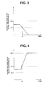
- a time t1 in Fig. 3 indicates a point in time when the supplied voltage becomes lower than the lower limit of 9 V.
- control element 21 may drive (duty control) sub-transistor 12 which so far was in condition of being turned off.
- driven (duty control) sub-transistor 12 can step down the power (having high voltage 42 V conveyed from high voltage wire A), and then supply the thus stepped down power to DC-DC converter 3, by way of sub-power supply wire D and second input terminal 31.
- the thus inputted power may then have its voltage smoothed by means of second capacitor 20, diode 17, and choke coil 18, to be outputted from output terminal 32.
- the duty ratio for driving sub-transistor 12 is so controlled as to bring about lowered voltage 14 V which is outputted from DC-DC converter 3.
- low voltage transistor 15 may cause a short mode failure.
- the short mode failure may keep low voltage transistor 15 turned on, thus disabling low voltage transistor 15 from the switching operation.
- the output voltage from DC-DC converter 3 may increase to high voltage 42 V which is the input voltage to DC-DC converter 3.
- the voltage supplied to first low voltage load 6A and second low voltage load 6B has the allowable range from 9 V to 16 V.
- control element 21 determines that the short mode failure has occurred to low voltage transistor 15.
- a time t2 in Fig. 4 indicates a point in time when the supplied voltage becomes higher than the upper limit of 16 V.
- control element 21 may turn off main transistor 11.
- control element 21 may, like in the open mode failure, drive (duty control) sub-transistor 12 which so far was in condition of being turned off. Thereby, DC-DC converter 3 can output lowered voltage 14 V from output terminal 32.
- control element 21 can warn a user of the open mode failure and the short mode failure of low voltage transistor 15.
- control element 21 Flow chart of operations by control element 21.
- Fig. 5 is a flow chart of operations by control element 21, according to the first embodiment.
- Step 101 Turning on main transistor 11 can supply the power to DC-DC converter 3 by way of main power supply wire C.
- control element 16 drives (duty control) low voltage transistor 15, to thereby output the power (having lowered voltage 14 V) from output terminal 32.
- Step 102 Control element 21 refers to voltage sensor 5 for the output voltage.
- Step 103 Control element 21 determines whether or not the output voltage sensed with voltage sensor 5 is lower than 9 V.
- Step 104 Control element 21 determines that low voltage transistor 15 in DC-DC converter 3 has caused the open mode failure.
- Step 105 Control element 21 turns on (lights up) warning lamp 8, thus warning the user of the open mode failure of low voltage transistor 15 in DC-DC converter 3.
- Step 106 Control element 21 drives (duty control) sub-transistor 12 so that the output voltage from DC-DC converter 3 can be equal to lowered voltage 14 V.
- step 103, step 104, step 105 and step 106 can secure the power having lowered voltage to be outputted from first low voltage load 6A and second low voltage load 6B.
- the routine may take the other steps as below:
- Step 107 Control element 21 determines whether or not the output voltage sensed with voltage sensor 5 is higher than 16 V.
- Step 108 Control element 21 determines that low voltage transistor 15 in DC-DC converter 3 has caused the short mode circuit.
- Step 109 Control element 21 turns off main transistor 11, to thereby stop supplying the power to DC-DC converter 3 by way of main power supply wire C. Then, the routine proceeds to subsequent step 105 and step 106.
- step 107, step 108, step 109, step 105, and step 106 can stop applying the power (having the voltage higher than 16 V) to first low voltage load 6A and second low voltage load 6B, thus preventing breakage.
- driving sub-transistor 12 can supply lowered voltage (proper voltage) continuously.
- step 101 to step 104 and step 106 to step 109 constitute a controlling means, while step 105 constitutes a warning section.
- the multi-voltage power supply system which is equipped with the high voltage system (42 V) and the low voltage system (14 V) according to the first embodiment of the present invention has the construction described above.
- driving sub-transistor 12 can secure supply of the output voltage to first low voltage load 6A and second low voltage load 6B even when the open mode failure and/or the short mode failure of low voltage transistor 15 may prevent supply of the power (having the lowered voltage) to first low voltage load 6A and second low voltage load 6B.
- the above construction of the multi-voltage power supply system according to the first embodiment of the present invention thereby, can save the need of a low voltage battery like the one that is used (against failures) for the multi-voltage power supply system as disclosed in "Automotive electronics power up”, IEEE SPECTRUM, May 2000.
- the low voltage battery is referred to as "12-V lead-acid battery” or "12-V battery” mainly on page 35 to page 37.
- the multi-voltage power supply system according to the first embodiment of the present invention can reduce cost and weight equivalent of the low voltage battery.
- turning off main transistor 11 in the short mode failure of low voltage transistor 15 can prevent supply of the power (having the high voltage) to first low voltage load 6A and second low voltage load 6B.
- checking (diagnosis) for any failure of sub-transistor 12 (which is driven for the switching operation when DC-DC converter 3 is in failure) at a proper timing, such as when the multi-voltage power supply system is turned on, can further increase reliability of the multi-voltage power supply system.
- Fig. 6 shows how control element 21 carries out the failure diagnosis of sub-transistor 12.
- Step 201 Control element 21 determines whether or not main transistor 11 is turned off.
- Step 207 Control element 21 turns off main transistor 11. Then, the routine proceeds to step 202.
- Step 202 Control element 21 drives sub-transistor 12 (duty control, for example, at the duty ratio of 33%) for the switching operation.
- sub-transistor 12 is to be used when DC-DC converter 3 is in failure.
- Step 203 Control element 21 refers to voltage sensor 5 for the output voltage.
- Step 204 Control element 21 determines whether or not the output voltage sensed with voltage sensor 5 is in the range from 9 V to 16 V.
- Step 205 Control element 21 determines that sub-transistor 12 is okay.
- Step 206 Control element 21 turns off sub-transistor 12 to stop the switching operation, thus completing the diagnosis of sub-transistor 12.
- the routine may take the other steps as below:
- Step 208 On the other hand, control element 21 determines that sub-transistor 12 is in failure.
- Step 209 Control element 21 turns off sub-transistor 12 to stop the switching operation.
- Step 210 Control element 21 conveys the signal to warning lamp 8, thus turning on (lighting up) the warning lamp 8 for warning the user of the failure of sub-transistor 12.
- warning lamp 8 is so adjusted as to operate in the following manner:
- Getting sub-transistor 12's information in advance by diagnosing sub-transistor 12 when turning on the power supply system can improve reliability of sub-transistor 12 which is driven when DC-DC converter 3 is in failure.
- FIG. 7 there is provided the circuit diagram showing the multi-voltage power supply system which is equipped with the high voltage system (42 V) and the low voltage system (14 V), according to a second embodiment of the present invention.
- a voltage sensor 5A according to the second embodiment is disposed in a position different from that of voltage sensor 5 (counterpart of voltage sensor 5A) according to the first embodiment in Fig. 2.
- power supply distributor 10A Like power supply distributor 10 according to the first embodiment, power supply distributor 10A according to the second embodiment connects to first high voltage load 4A and second high voltage load 4B. Moreover, power supply distributor 10A connects to DC-DC converter 3, by way of main power supply wire C and sub-power supply wire D. DC-DC converter 3 connects to first low voltage load 6A and second low voltage load 6B by way of output wire B.
- control element 21A can control main transistor 11 and sub-transistor 12.
- the short mode failure caused to low voltage transistor 15 in DC-DC converter 3 may keep low voltage transistor 15 turned on, thus disabling low voltage transistor 15 from the switching operation.
- voltage sensor 5A senses the input voltage (high voltage 42 V) of DC-DC converter 3 showing no change (constant), as is seen in Fig. 8.
- the sensed signal can be inputted to control element 21A by way of signal wire F. If high voltage 42 V sensed with voltage sensor 5A continues for at least a predetermined time X, control element 21A determines that low voltage transistor 15 has caused the short mode failure.
- Predetermined time X can be set, for example, in the following manner:
- the open mode failure caused to low voltage transistor 15 in DC-DC converter 3 may keep low voltage transistor 15 turned off, thus disabling low voltage transistor 15 from the switching operation.
- voltage sensor 5A senses voltage 0 V showing no change (constant), as is seen in Fig. 9.
- the sensed signal can be inputted to control element 21A by way of signal wire F. If the voltage 0 V sensed with voltage sensor 5A continues for at least a predetermined time X', control element 21A determines that low voltage transistor 15 has caused the open mode failure.
- Predetermined time X' can be set, for example, in the following manner:
- control element 21A Flow chart of operations by control element 21A
- Fig. 10 is a flow chart of operations by control element 21A, according to the second embodiment.
- Step 301 Control element 21A turns on main transistor 11, to thereby input the power (having high voltage 42 V) to DC-DC converter 3 by way of main power supply wire C.
- Driving low voltage transistor 15 can step down high voltage 42 V of the thus inputted power to lowered voltage 14V.
- Step 302 Control element 21A refers to voltage sensor 5A for the voltage.
- Step 303 Control element 21A determines whether or not high voltage 42 V continues for at least predetermined time X. If YES at step 303, the routine proceeds to step 304. If NO at step 303, the routine proceeds to step 308.
- Step 304 Control element 21A determines that low voltage transistor 15 in DC-DC converter 3 has caused the short mode failure.
- Step 305 Control element 21A turns off main transistor 11, thus stopping the supply of the power to DC-DC converter 3.
- Step 306 Control element 21A turns on (lights up) warning lamp 8, warning the user of the short mode failure of low voltage transistor 15.
- Step 307 Control element 21A drives (duty control) sub-transistor 12 so that the output voltage can be securely supplied to first low voltage load 6A and second low voltage load 6B.
- the routine may take the other steps as below:
- Step 308 Control element 21A determines whether or not voltage 0 V continues for at least predetermined time X'. If YES at step 308, the routine proceeds to step 309. If NO at step 308, the routine returns to step 302.
- Step 309 Control element 21A determines that low voltage transistor 15 in DC-DC converter 3 has caused the open mode failure. Then, the routine proceeds to the subsequent step 306 and step 307.
- control element 21A The above operations of control element 21A can be summarized as below:
- the following feature of the multi-voltage power supply system according to the second embodiment of the present invention can contribute to shortening signal wire F between voltage sensor 5A and control element 21A:
- the short mode failure when the short mode failure is caused to low voltage transistor 15, it is sub-transistor 12 that is driven in duty control for supplying the power ⁇ having lowered voltage ⁇ to first low voltage load 6A and second low voltage load 6B.
- Main transistor 11 can replace sub-transistor 12 to be driven in duty control for stepping down high voltage from high voltage power supply 1 so that lowered voltage can be outputted to first low voltage load 6A and second low voltage load 6B.
- the number of high voltage loads is two. More specifically, first high voltage load 4A and second high voltage load 4B according to the first embodiment connect to power supply distributor 10, while first high voltage load 4A and second high voltage load 4B according to the second embodiment connect to power supply distributor 10A.
- the number of high voltage loads is, however, not limited to two. The number of high voltage loads can be determined on a case-by-case basis.
- the number of low voltage loads can be determined on a case-by-case basis.
- the transistor used as the switching element can be replaced with other devices.
- the method of diagnosing sub-transistor 12 is not limited to the one shown in Fig. 6.
- the following method is replaceable:
Landscapes
- Engineering & Computer Science (AREA)
- Power Engineering (AREA)
- Dc-Dc Converters (AREA)
- Charge And Discharge Circuits For Batteries Or The Like (AREA)
Applications Claiming Priority (2)
| Application Number | Priority Date | Filing Date | Title |
|---|---|---|---|
| JP2002005118A JP3610950B2 (ja) | 2002-01-11 | 2002-01-11 | 電源装置 |
| JP2002005118 | 2002-01-11 |
Publications (3)
| Publication Number | Publication Date |
|---|---|
| EP1328053A2 true EP1328053A2 (de) | 2003-07-16 |
| EP1328053A3 EP1328053A3 (de) | 2004-06-23 |
| EP1328053B1 EP1328053B1 (de) | 2006-02-22 |
Family
ID=19191066
Family Applications (1)
| Application Number | Title | Priority Date | Filing Date |
|---|---|---|---|
| EP02258406A Expired - Lifetime EP1328053B1 (de) | 2002-01-11 | 2002-12-05 | Stromversorgungssystem |
Country Status (4)
| Country | Link |
|---|---|
| US (1) | US6803749B2 (de) |
| EP (1) | EP1328053B1 (de) |
| JP (1) | JP3610950B2 (de) |
| DE (1) | DE60209317T2 (de) |
Cited By (1)
| Publication number | Priority date | Publication date | Assignee | Title |
|---|---|---|---|---|
| EP2830180A1 (de) * | 2013-07-26 | 2015-01-28 | Hamilton Sundstrand Corporation | Isolierte Gleichstrom-Gleichstrom-Stromversorgung von Nichttransformatortyp einschließlich Abschaltschaltung |
Families Citing this family (10)
| Publication number | Priority date | Publication date | Assignee | Title |
|---|---|---|---|---|
| EP1483824A2 (de) * | 2002-02-26 | 2004-12-08 | Philips Intellectual Property & Standards GmbH | Verfahren zum betrieben eines schaltnetzteils und schaltnetzteil |
| US7015678B2 (en) * | 2004-06-22 | 2006-03-21 | Dialog Semiconductor Gmbh | Efficiency improvement of DC-DC converter |
| JP4545514B2 (ja) * | 2004-08-05 | 2010-09-15 | 本田技研工業株式会社 | 電圧変換器の制御方法 |
| JP4812529B2 (ja) * | 2006-06-14 | 2011-11-09 | トヨタ自動車株式会社 | 電源装置および車両 |
| EP2330728A4 (de) * | 2008-09-22 | 2014-11-26 | Fujitsu Ltd | Leistungsregelschaltung, stromversorgungseinheit, stromversorgungssystem und leistungsregler-steuerverfahren |
| JP5464910B2 (ja) * | 2009-05-28 | 2014-04-09 | 三菱電機株式会社 | 電力変換装置 |
| JP5645425B2 (ja) * | 2010-02-26 | 2014-12-24 | 三菱電機株式会社 | 電力変換装置 |
| JP4630952B1 (ja) * | 2010-06-14 | 2011-02-09 | オーナンバ株式会社 | 直流安定化電源装置 |
| CN109902410B (zh) * | 2019-03-07 | 2023-05-05 | 上海华虹宏力半导体制造有限公司 | 一种检查低压晶体管可靠性的方法 |
| CN115362612A (zh) * | 2020-04-06 | 2022-11-18 | 日产自动车株式会社 | 蓄电池异常警告方法及蓄电池异常警告装置 |
Citations (2)
| Publication number | Priority date | Publication date | Assignee | Title |
|---|---|---|---|---|
| US6037755A (en) * | 1998-07-07 | 2000-03-14 | Lucent Technologies Inc. | Switching controller for a buck+boost converter and method of operation thereof |
| EP1033804A2 (de) * | 1999-03-02 | 2000-09-06 | Delphi Technologies, Inc. | Elektrisches Doppelspannungsfahrzeugssystem mit unterresonantem Gleichstrom-Gleichstromwandler |
Family Cites Families (6)
| Publication number | Priority date | Publication date | Assignee | Title |
|---|---|---|---|---|
| US5481178A (en) * | 1993-03-23 | 1996-01-02 | Linear Technology Corporation | Control circuit and method for maintaining high efficiency over broad current ranges in a switching regulator circuit |
| US6400126B1 (en) * | 1999-12-30 | 2002-06-04 | Volterra Semiconductor Corporation | Switching regulator with multiple power transistor driving voltages |
| US6650098B2 (en) * | 2000-08-24 | 2003-11-18 | International Rectifier Corporation | Current limited buck power supply |
| JP3706810B2 (ja) * | 2001-05-23 | 2005-10-19 | 株式会社ルネサステクノロジ | Dc−dcコンバータとその制御回路 |
| JP3776752B2 (ja) * | 2001-06-07 | 2006-05-17 | 新電元工業株式会社 | Dc−dcコンバータ |
| US6600298B2 (en) * | 2001-10-31 | 2003-07-29 | Dell Products L.P. | Switching DC-DC converter with the output voltage changing inversely to any change in the converter inductor current |
-
2002
- 2002-01-11 JP JP2002005118A patent/JP3610950B2/ja not_active Expired - Fee Related
- 2002-12-05 DE DE60209317T patent/DE60209317T2/de not_active Expired - Lifetime
- 2002-12-05 EP EP02258406A patent/EP1328053B1/de not_active Expired - Lifetime
-
2003
- 2003-01-08 US US10/337,735 patent/US6803749B2/en not_active Expired - Fee Related
Patent Citations (2)
| Publication number | Priority date | Publication date | Assignee | Title |
|---|---|---|---|---|
| US6037755A (en) * | 1998-07-07 | 2000-03-14 | Lucent Technologies Inc. | Switching controller for a buck+boost converter and method of operation thereof |
| EP1033804A2 (de) * | 1999-03-02 | 2000-09-06 | Delphi Technologies, Inc. | Elektrisches Doppelspannungsfahrzeugssystem mit unterresonantem Gleichstrom-Gleichstromwandler |
Non-Patent Citations (3)
| Title |
|---|
| BIGORRA ET AL: "Dual-Voltage Power Networks" AUTOMOTIVE ENGINEERING, SAE, vol. 108, no. 9, September 2000 (2000-09), pages 113-116, XP000959225 Warrendale US * |
| KASSAKIAN ET AL: "Automotive Electronics Power Up" IEEE SPECTRUM, vol. 37, no. 5, May 2000 (2000-05), pages 34-39, XP001030270 * |
| KHAN I A: "Power electronics in automotive electrical systems" POWER ELECTRONICS IN TRANSPORTATION, IEEE, 24 October 1996 (1996-10-24), pages 29-38, XP010207836 Dearborn MI USA * |
Cited By (2)
| Publication number | Priority date | Publication date | Assignee | Title |
|---|---|---|---|---|
| EP2830180A1 (de) * | 2013-07-26 | 2015-01-28 | Hamilton Sundstrand Corporation | Isolierte Gleichstrom-Gleichstrom-Stromversorgung von Nichttransformatortyp einschließlich Abschaltschaltung |
| US9438100B2 (en) | 2013-07-26 | 2016-09-06 | Hamilton Sundstrand Corporation | Non-transformer isolated DC-DC power supply including shut down circuit |
Also Published As
| Publication number | Publication date |
|---|---|
| EP1328053A3 (de) | 2004-06-23 |
| US6803749B2 (en) | 2004-10-12 |
| US20030133240A1 (en) | 2003-07-17 |
| JP2003209968A (ja) | 2003-07-25 |
| DE60209317T2 (de) | 2006-10-05 |
| DE60209317D1 (de) | 2006-04-27 |
| EP1328053B1 (de) | 2006-02-22 |
| JP3610950B2 (ja) | 2005-01-19 |
Similar Documents
| Publication | Publication Date | Title |
|---|---|---|
| US20210122244A1 (en) | Power supply system | |
| US11133702B2 (en) | Vehicle power supply system | |
| US8269641B2 (en) | Vehicle power management system | |
| US7075237B2 (en) | Illumination control apparatus and failure detecting apparatus | |
| US6803749B2 (en) | Power supply system and process including sub-switching element control | |
| US20030032308A1 (en) | Electrical connection system for vehicle | |
| JP7421308B2 (ja) | 車両の電源管理装置及び方法 | |
| US5798629A (en) | Apparatus for diagnosing low voltage battery | |
| US8963376B2 (en) | Electrical load driving apparatus | |
| EP2183945B1 (de) | Durch ein remote einschaltbares vorspannungsnetzteil gesteuerte metallhalidlampenladung | |
| US11059439B2 (en) | In-vehicle power supply device | |
| JP2005206085A (ja) | 電力分配システム、電力分配器、及びブレーキ装置 | |
| JP5134838B2 (ja) | 車両用電源装置 | |
| JP3679700B2 (ja) | 車両用ランプ制御装置 | |
| JP2002171691A (ja) | デュアル電圧対応車両制御装置 | |
| US6580219B1 (en) | Electrical control circuit for a switched load | |
| EP1088702B1 (de) | Steuerungsanordnung für das Stromversorgungsystem eines Fahrzeugs | |
| JP2011100667A (ja) | 点灯装置及びそれを用いた前照灯、車輌 | |
| US20130076125A1 (en) | Load control device | |
| JP2002252935A (ja) | 車両用電源システム | |
| US6472829B2 (en) | Discharge lamp lighting circuit | |
| JP2002144958A (ja) | 車両用ランプの点灯制御装置 | |
| KR102699786B1 (ko) | 암전류를 최소화하는 차량 전원 분배 회로의 이상 감지 회로 및 이상 감지 방법 | |
| WO2022131341A1 (ja) | スイッチ駆動回路 | |
| US20010043072A1 (en) | Programmable electronic flasher relays |
Legal Events
| Date | Code | Title | Description |
|---|---|---|---|
| PUAI | Public reference made under article 153(3) epc to a published international application that has entered the european phase |
Free format text: ORIGINAL CODE: 0009012 |
|
| 17P | Request for examination filed |
Effective date: 20021216 |
|
| AK | Designated contracting states |
Designated state(s): AT BE BG CH CY CZ DE DK EE ES FI FR GB GR IE IT LI LU MC NL PT SE SI SK TR |
|
| AX | Request for extension of the european patent |
Extension state: AL LT LV MK RO |
|
| PUAL | Search report despatched |
Free format text: ORIGINAL CODE: 0009013 |
|
| AK | Designated contracting states |
Kind code of ref document: A3 Designated state(s): AT BE BG CH CY CZ DE DK EE ES FI FR GB GR IE IT LI LU MC NL PT SE SI SK TR |
|
| AX | Request for extension of the european patent |
Extension state: AL LT LV MK RO |
|
| RIC1 | Information provided on ipc code assigned before grant |
Ipc: 7H 02M 3/00 B Ipc: 7H 02J 7/14 A |
|
| 17Q | First examination report despatched |
Effective date: 20041221 |
|
| AKX | Designation fees paid |
Designated state(s): DE FR GB |
|
| GRAP | Despatch of communication of intention to grant a patent |
Free format text: ORIGINAL CODE: EPIDOSNIGR1 |
|
| GRAS | Grant fee paid |
Free format text: ORIGINAL CODE: EPIDOSNIGR3 |
|
| GRAA | (expected) grant |
Free format text: ORIGINAL CODE: 0009210 |
|
| AK | Designated contracting states |
Kind code of ref document: B1 Designated state(s): DE FR GB |
|
| REG | Reference to a national code |
Ref country code: GB Ref legal event code: FG4D |
|
| REF | Corresponds to: |
Ref document number: 60209317 Country of ref document: DE Date of ref document: 20060427 Kind code of ref document: P |
|
| ET | Fr: translation filed | ||
| PLBE | No opposition filed within time limit |
Free format text: ORIGINAL CODE: 0009261 |
|
| STAA | Information on the status of an ep patent application or granted ep patent |
Free format text: STATUS: NO OPPOSITION FILED WITHIN TIME LIMIT |
|
| 26N | No opposition filed |
Effective date: 20061123 |
|
| PGFP | Annual fee paid to national office [announced via postgrant information from national office to epo] |
Ref country code: GB Payment date: 20131204 Year of fee payment: 12 Ref country code: DE Payment date: 20131127 Year of fee payment: 12 |
|
| PGFP | Annual fee paid to national office [announced via postgrant information from national office to epo] |
Ref country code: FR Payment date: 20131209 Year of fee payment: 12 |
|
| REG | Reference to a national code |
Ref country code: DE Ref legal event code: R119 Ref document number: 60209317 Country of ref document: DE |
|
| GBPC | Gb: european patent ceased through non-payment of renewal fee |
Effective date: 20141205 |
|
| REG | Reference to a national code |
Ref country code: FR Ref legal event code: ST Effective date: 20150831 |
|
| PG25 | Lapsed in a contracting state [announced via postgrant information from national office to epo] |
Ref country code: GB Free format text: LAPSE BECAUSE OF NON-PAYMENT OF DUE FEES Effective date: 20141205 Ref country code: DE Free format text: LAPSE BECAUSE OF NON-PAYMENT OF DUE FEES Effective date: 20150701 |
|
| PG25 | Lapsed in a contracting state [announced via postgrant information from national office to epo] |
Ref country code: FR Free format text: LAPSE BECAUSE OF NON-PAYMENT OF DUE FEES Effective date: 20141231 |