EP1324397A2 - Optisches Modul - Google Patents
Optisches Modul Download PDFInfo
- Publication number
- EP1324397A2 EP1324397A2 EP02028865A EP02028865A EP1324397A2 EP 1324397 A2 EP1324397 A2 EP 1324397A2 EP 02028865 A EP02028865 A EP 02028865A EP 02028865 A EP02028865 A EP 02028865A EP 1324397 A2 EP1324397 A2 EP 1324397A2
- Authority
- EP
- European Patent Office
- Prior art keywords
- base
- photo detector
- optical module
- wiring patterns
- circumferential surface
- Prior art date
- Legal status (The legal status is an assumption and is not a legal conclusion. Google has not performed a legal analysis and makes no representation as to the accuracy of the status listed.)
- Granted
Links
Images


Classifications
-
- H—ELECTRICITY
- H10—SEMICONDUCTOR DEVICES; ELECTRIC SOLID-STATE DEVICES NOT OTHERWISE PROVIDED FOR
- H10F—INORGANIC SEMICONDUCTOR DEVICES SENSITIVE TO INFRARED RADIATION, LIGHT, ELECTROMAGNETIC RADIATION OF SHORTER WAVELENGTH OR CORPUSCULAR RADIATION
- H10F77/00—Constructional details of devices covered by this subclass
- H10F77/50—Encapsulations or containers
-
- G—PHYSICS
- G02—OPTICS
- G02B—OPTICAL ELEMENTS, SYSTEMS OR APPARATUS
- G02B6/00—Light guides; Structural details of arrangements comprising light guides and other optical elements, e.g. couplings
- G02B6/24—Coupling light guides
- G02B6/42—Coupling light guides with opto-electronic elements
- G02B6/4201—Packages, e.g. shape, construction, internal or external details
-
- H—ELECTRICITY
- H10—SEMICONDUCTOR DEVICES; ELECTRIC SOLID-STATE DEVICES NOT OTHERWISE PROVIDED FOR
- H10F—INORGANIC SEMICONDUCTOR DEVICES SENSITIVE TO INFRARED RADIATION, LIGHT, ELECTROMAGNETIC RADIATION OF SHORTER WAVELENGTH OR CORPUSCULAR RADIATION
- H10F30/00—Individual radiation-sensitive semiconductor devices in which radiation controls the flow of current through the devices, e.g. photodetectors
- H10F30/20—Individual radiation-sensitive semiconductor devices in which radiation controls the flow of current through the devices, e.g. photodetectors the devices having potential barriers, e.g. phototransistors
- H10F30/21—Individual radiation-sensitive semiconductor devices in which radiation controls the flow of current through the devices, e.g. photodetectors the devices having potential barriers, e.g. phototransistors the devices being sensitive to infrared, visible or ultraviolet radiation
- H10F30/22—Individual radiation-sensitive semiconductor devices in which radiation controls the flow of current through the devices, e.g. photodetectors the devices having potential barriers, e.g. phototransistors the devices being sensitive to infrared, visible or ultraviolet radiation the devices having only one potential barrier, e.g. photodiodes
- H10F30/223—Individual radiation-sensitive semiconductor devices in which radiation controls the flow of current through the devices, e.g. photodetectors the devices having potential barriers, e.g. phototransistors the devices being sensitive to infrared, visible or ultraviolet radiation the devices having only one potential barrier, e.g. photodiodes the potential barrier being a PIN barrier
-
- H—ELECTRICITY
- H10—SEMICONDUCTOR DEVICES; ELECTRIC SOLID-STATE DEVICES NOT OTHERWISE PROVIDED FOR
- H10F—INORGANIC SEMICONDUCTOR DEVICES SENSITIVE TO INFRARED RADIATION, LIGHT, ELECTROMAGNETIC RADIATION OF SHORTER WAVELENGTH OR CORPUSCULAR RADIATION
- H10F55/00—Radiation-sensitive semiconductor devices covered by groups H10F10/00, H10F19/00 or H10F30/00 being structurally associated with electric light sources and electrically or optically coupled thereto
-
- H—ELECTRICITY
- H10—SEMICONDUCTOR DEVICES; ELECTRIC SOLID-STATE DEVICES NOT OTHERWISE PROVIDED FOR
- H10F—INORGANIC SEMICONDUCTOR DEVICES SENSITIVE TO INFRARED RADIATION, LIGHT, ELECTROMAGNETIC RADIATION OF SHORTER WAVELENGTH OR CORPUSCULAR RADIATION
- H10F77/00—Constructional details of devices covered by this subclass
- H10F77/93—Interconnections
-
- G—PHYSICS
- G02—OPTICS
- G02B—OPTICAL ELEMENTS, SYSTEMS OR APPARATUS
- G02B6/00—Light guides; Structural details of arrangements comprising light guides and other optical elements, e.g. couplings
- G02B6/24—Coupling light guides
- G02B6/42—Coupling light guides with opto-electronic elements
- G02B6/4292—Coupling light guides with opto-electronic elements the light guide being disconnectable from the opto-electronic element, e.g. mutually self aligning arrangements
Definitions
- This invention relates to an optical module on which a radiative device and a photo detector for detecting emitted light or the like are mounted.
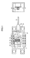
- FIG. 22 A is a top view showing a conventional optical module.
- FIG. 22B is a side view showing a conventional optical module.
- FIG. 22C is a front view showing a PD element.
- reference numeral 1 denotes a substrate on which an LD carrier 3 and a PD carrier are mounted, 2 a radiative device (hereinafter referred to as an LD element, not shown), 3 an LD carrier for holding thereon the LD element 2, 4 a photo detector (hereinafter referred to as a PD element) for detecting back light from the LD element 2, 4a an incident surface of the PD element, at the peripheral of which an anode electrode 4b is provided, and on the opposite surface of which a cathode electrode is provided.
- a PD element photo detector
- Reference numeral 5 denotes a PD carrier for holding thereon the PD element 4, 5a, 5b wiring patterns laid out on the PD carrier 5, 6 a wire bonding for electrically connecting the anode element 4b of the PD element 4 to the wiring pattern 5a, and 7, 8 wire bondings for electrically connecting wiring patterns of a package (not shown) which holds thereon the substrate 1 to the wiring patterns 5a, 5b.
- the conventional optical module has been mounted the PD element 4 on the PD carrier 5 such that the incident surface 4a of the PD element 4 faces to the back of the LD element 2.
- the anode electrode 4b is electrically connected to the wiring pattern 5a of the PD carrier 5 by the wire bonding. Further, the wiring patterns of the package (not shown) which holds thereon the substrate 1 are electrically connected to the wiring patterns 5a, 5b by the wire bondings 7, 8.
- the conventional optical module thus configured as above involves numerous troublesome wire bonding processes required for manufacturing of an optical module. Further, the PD carrier has to be mounted to mount the PD element 4 on the substrate 1. Thus, this requirement invites a bulky and costly optical module, and asks for an additional mounting process for the PD carrier 5.
- the present invention has been made to solve the above problems and an object thereof is to provide an optical module able to eliminate the PD carrier and simplify the manufacturing process.
- an optical module in which an electrode of a photo detector for detecting emitted light from a radiative device is electrically connected to wiring patterns, and in which a conductive coupling member is provided for securing the photo detector to a base.
- an optical module in which an electrode of a photo detector for detecting emitted light from an optical fiber is electrically connected to wiring patterns, and in which a conductive coupling member is provided for securing the photo detector to a base.
- an optical module in which solder is applied to solder an electrode of a photo detector for detecting emitted light from an optical fiber and wiring patterns.
- an optical module in which solder is applied to solder an electrode of a photo detector for detecting emitted light from a radiative device and wiring patterns.
- an optical module in which a conductive adhesive is applied to adhere an electrode of a photo detector for detecting emitted light from a radiative device to wiring patterns.
- an optical module in which a conductive adhesive is applied to adhere an electrode of a photo detector for detecting emitted light from an optical fiber to wiring patterns.
- the dimension of a photo detector is determined so that the intensity center of emitted light substantially coincides with the center of an incident surface of the photo detector.
- a slit is formed to insert thereinto a part of a photo detector.
- the slit is formed in U-shape.
- the slit is formed in V-shape.
- the depth of the slit is set so that emitted light impinges on the center of the incident surface of the photo detector.
- the incident surface of the photo detector stood on the slant relative to emitted light.
- a stepwise slit whose center line is shifted in stages is formed on a base, into which a part of the photo detector is inserted.
- two grooves are formed on the surface with which the photo detector is contacted.
- the height of the photo detector is set to be smaller than twice of the width thereof.
- an insulating layer is provided on the periphery of the incident surface of the photo detector.
- an insulating film is coated on the circumference of the photo detector which is contacted with the base.
- the wire when a wire is laid out on one side of a couple of electrode layers of the photo detector, the wire is connected to the wiring patterns.
- an optical module including a base on which wiring patterns are laid out, and an optical fiber for carrying front emitted light from the radiative device.
- an optical module in which a package is provided to hold a base on which wiring patterns are laid out, and an optical fiber through which light to be impinged on the photo detector is carried.
- holding means is provided for removably holding the optical fiber.
- a lens is placed between the radiative device and the optical fiber.
- a lens is placed between the optical fiber and the photo detector.
- the electrode which detects emitted light from the radiative device is electrically connected to the wiring patterns and is provided with the conductive coupling member so as to secure the detecting device to the base, the detecting device can be mounted without relying on the PD carrier. As a result, this simplifies manufacturing processes.
- FIG. 1 is an overall block diagram showing an optical module according to the first embodiment of the present invention.
- FIG. 2A is a top view showing a purview of an optical module according to the first embodiment.
- FIG. 2B is a rear view showing a PD element.
- FIG. 2C is a side view showing a purview of an optical module.
- Fig. 2D is a front view showing a PD element.
- reference numeral 11 denotes a dielectric substrate (base) on which wiring patterns 11a, 11b are laid out, 12 an LD element (radiative device) for emitting light to an optical fiber 21, 13 an LD carrier for holding thereon the LD element 12, 14 a PD element (photo detector) for detecting back light (emitted light) emitted from the LD element 12, 14a an incident surface of the PD element 14, 14b an anode electrode provided at the periphery of the photo detector 14a, 14c a cathode electrode provided on the back of the PD element 14.
- Reference numeral 15 denotes solder (conductive coupling member) for electrically connecting an anode electrode 14b of the PD element 14 to wiring patterns 11a of the dielectric substrate 11, and for securing the PD element to the dielectric substrate 11, 16 solder (conductive coupling member) for electrically connecting a cathode electrode 14c of the PD element 14 to wiring patterns 11b of the dielectric substrate 11, and for securing the PD element 14 to the dielectric substrate 11.
- solder conductive coupling member
- Reference numeral 17 denotes a package which holds thereon the dielectric substrate 11 and the optical fiber 21 or the like, 18 a wiring pattern laid out on the package 17, 19a, 19b wire bonding for electrically connecting wiring patterns 19a, 19b to wiring patterns 11a, 11b, 20 a lens placed between the LD element 12 and the optical fiber 21 to efficiently transmit front light emitted from the LD element 12, 21 an optical fiber for carrying front light emitted from the LD element 12, 22 a ferrule for securing the optical fiber 21, 23 a ferrule holder for holding the ferule 22, and 24 a hermetic window.
- FIG. 3 is an explanatory view showing a concept of a PD monitor.
- a circuit is designed in the following.
- the PD element 14 detects back light emitted from the LD element 12
- the PD element 14 outputs an electrical signal, whose magnitude is proportional to that of back light, to an external Automatic Power-Control (APC) circuit 51.
- the APC circuit controls a light output level of the LD element 12 via a driver IC 52.
- a driver IC 52 For example, in case the magnitude of back light emitted from the LD element 12 is greater than that of the established one, a drive current for the LD element 12 is reduced so that the optical output level becomes small. Conversely, in case back light emitted from the LD element 12 is smaller than the established one, the drive current for the LD element 12 is reduced so that the light output level of the LD element 12 becomes large.
- the driver IC 52 is sometimes provided outside of the package 17.
- the Pd element 14 stood on the dielectric substrate 11 such that the incident surface 14a of the PD element 14 faces to the back surface.
- the PD element 14 in order for the PD element 14 to surely detect back light, suppose that the dimension of the PD element 14 is set so that back light emitted from the LD element 12 impinges on the center of the incident surface 14a of the PD element 14.
- the anode electrode 14b of the PD element 14 is electrically and mechanically connected to the wiring pattern 11a of the dielectric substrate 11 by the solder 15.
- the cathode electrode 14c of the PD element 14 is electrically and mechanically connected to the wiring patterns 11b of the dielectric substrate 11 by the solder 16.
- the PD element 14 can be mounted, without relying on the PD carrier. As a result, this obviates a wire bonding process for bonding the anode electrode 14b and the PD carrier, and a mounting process for the PD carrier, thus simplifying manufacturing processes.
- solders 15, 16 are adopted, but, needless to say, without being limited thereto, a conductive adhesive may be used, as an alternative, for example.
- the PD element 14 detects back light emitted from the LD element 12, but, as a matter of course, without being limited thereto, the LD element 14 may detect a part of front light emitted from the LD element 12.
- the optical fiber 21 is secured to the package 17, but, as shown in FIG. 4, a receptacle (holding means) may be provided, as an alternative, in the package 17 for removably holding the ferrule 22 by which the optical fiber 21 is fixed. This connects and disconnects the optical fiber 21 to/from the optical fiber at need.
- FIG. 4 is an overall block diagram showing an optical module according to the second embodiment of the present invention.
- reference numeral 27 denotes a space into which the ferrule 22 is inserted, 28 a hole with which an optical path is formed.
- FIG. 5 is an overall block diagram showing an optical module according to the second embodiment.
- reference numeral 5 denotes a sealing compound.
- the lens 20 is placed between the LD element 12 and the optical fiber 21.
- the lens 20 is not mandatory.
- FIG. 6 is an overall block diagram showing an optical module according the third embodiment of the present invention.
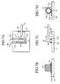
- FIG. 7A is a top view showing a purview of an optical module according to the third embodiment.
- FIG. 7B is a rear view showing a PD element.
- FIG. 7C is a side view showing a purview of an optical module.
- FIG. 7D is a front view showing a PD element.
- FIGS. 7A through 7D the same reference numerals as those in FIGS. 2, 5 indicate identical or equivalent parts and therefore descriptions thereof are omitted for brevity s sake.
- reference numeral 30 denotes an optical fiber carrier for holding thereon the optical fiber.
- the PD element 14 detects front light or back light emitted from the LD element 12.
- the PD module 14 may detect emitted light from the optical fiber 21.
- FIG. 8 is an overall block diagram showing an optical module according to the fourth embodiment of the present invention.
- FIG. 9 is an overall block diagram showing an optical module according to the fourth embodiment.
- the lens is not placed between the optical fiber 21 and the PD element 14.
- the lens 20 may be placed between the optical fiber 21 and the PD element 15.
- the optical fiber 21 is secured to the package 17.
- a receptacle 26 may be provided for removably holding the ferrule 22 by which the optical fiber 21 is fixed. This gives freedom to connect and disconnect the optical fiber 21 to/from the optical module at need.
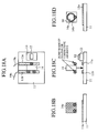
- FIG. 10A is a top view showing a purview of an optical module according to the fifth embodiment.
- FIG. 10B is a rear view showing a PD element.
- FIG. 10C is a side view showing a purview of an optical module.
- FIG. 10D is a front view showing a PD element.
- the same reference numerals as those in FIG. 2 indicate identical or equivalent parts and therefore descriptions thereof are omitted for brevity s sake.
- reference numeral 31 denotes a slit into which a part of the PD element 14 is inserted, and which is formed in V-shape.
- Reference numeral 32 denotes a clearance between the PD element 14 and the dielectric substrate 11, which is created when the PD element 14 is inserted into the slit 31.
- the PD element 14 stood on the dielectric substrate 11 without forming a slit on the dielectric substrate 11. In this event, in case the PD element 14 is not held by a jig, it would be difficult to stand the PD element 14, in pouring the solders 15, 16 or the conductive adhesive into the slit.
- the slit 31 into which a part of the PD element 14 is inserted is formed on the substrate 11 so as to stand the PD element 14 in the slit 31, in pouring the solders 15, 16 or the conductive adhesive into the slit.
- the slit 31 is formed in V-shape.
- a clearance 32 is created between the PD element 14 and the dielectric substrate 11.
- solder 15, 16 may perhaps be poured between the PD element 14 and the dielectric substrate 11 from capillarity, which causes short-circuiting between the anode electrode 14b and the cathode electrode 14c.
- the solders 15, 16 do not pour into the base of the PD element 14 anymore from capillarity, which frees from danger of the short-circuiting between the anode electrode 14b and the cathode electrode 14c.
- the slit 31 is formed in V-shape, but, needless to say, without being limited thereto, the slit 31 may be formed in U-shape, as an alternative, for example.
- the PD element 14 stood on the dielectric substrate 11 such that the incident surface 14a of the PD element 14 faces to the back of the LD element 12 or the optical fiber 21.
- the incident surface 14a of the PD element 14 may stand on the slant relative to the back of the LD element 12 or the optical fiber 21.
- the slant angle of the PD element 14 is not limited to any specific one. Generally, it is within the range from 0° to 20°, preferably, from 4° to 12°. This reduces the amount of light reflected from the incident surface 14a of the PD element 14 to the LD element 12.
- the incident surface 14a of the PD element 14 stood on the slant relative to the back of the LD element 12 or the optical fiber 21.
- slits whose center of grooves are shifted in stages may be formed on the dielectric substrate 11.
- the PD element 14 will be able successfully to not only mount it on the slant but also manufacture the dielectric substrate 11 having repeatedly formed grooves in the working process. This permits manufacturing of the large substrate by one working process.
- the incident surface 14a of the PD element 14 stood relative to the back of the LD element 12 or the optical fiber 21.
- two grooves may be formed on the surface of the dielectric substrate 11 with which the PD element 12 is contacted. This prevents from short-circuiting between the anode electrode 14b and the cathode electrode 14c.
- the height of the PD element 14 may be set to be smaller than twice of the width T thereof.
- a bump made of solder or conductive adhesive may be previously formed to adhere to the anode electrode 14b and the cathode electrode 14c of the PD element 14. Thereafter, the PD element 14 may be mounted on the dielectric substrate 11.
- the incident surface 14a of the PD element 14 is formed by p layer, the back n layer, and an intermediate layer between the incident surface 14a and the back i layer.
- the P layer is electrically connected to the n layer, with short-circuiting being occurred between the anode electrode 14b and the cathode electrode 14c.
- a PD element is formed, in which an insulating layer 14d is embedded into the periphery of the incident surface 14a.
- an insulating material polyimide or Fe doped InP is advisable. This prevents from short-circuiting between the anode electrode 14b and the cathode electrode 14c by doing away with pn connection, as the insulating layer 14b is embedded into the mounting surface of the dielectric substrate 11 on which the PD element 14 is to be mounted, even if the solder 15, 16 are poured between the PD element 14 and the dielectric substrate 11 from capillarity.
- the insulating layer 14e is formed on the mounting surface on which the PD element 14 is to be mounted in AR coat or HR coat manner.
- S i O 2 used for AR coat is desirable, for example. This exerts same effect as the eleventh embodiment.
- both electrodes are electrically connected to the wiring patterns 11a, 11b with the solder or the conductive adhesive, but, one electrode may be connected to the wiring patterns without relying on the solder or the conductive adhesive.
- the PD element to which awire 33 is previously attached is provided at the anode electrode 14b.
- the previous lay out of the wire 33 is carried out in the fashion of wire bonding and then wire is cut by torch and the like.
- a big solder bole is put on the back of the PD element 14 to thereby electrically connect the cathode electrode 14c to the wiring patterns 11b.
- the wire 33 is compression bonded on the wiring patterns 11a to electrically connect the anode electrode 14b to the wiring patterns 11a.
Landscapes
- Physics & Mathematics (AREA)
- General Physics & Mathematics (AREA)
- Optics & Photonics (AREA)
- Optical Couplings Of Light Guides (AREA)
- Semiconductor Lasers (AREA)
- Light Receiving Elements (AREA)
Applications Claiming Priority (2)
| Application Number | Priority Date | Filing Date | Title |
|---|---|---|---|
| JP2001401464A JP4166471B2 (ja) | 2001-12-28 | 2001-12-28 | 光モジュール |
| JP2001401464 | 2001-12-28 |
Publications (3)
| Publication Number | Publication Date |
|---|---|
| EP1324397A2 true EP1324397A2 (de) | 2003-07-02 |
| EP1324397A3 EP1324397A3 (de) | 2007-07-11 |
| EP1324397B1 EP1324397B1 (de) | 2012-02-15 |
Family
ID=19189781
Family Applications (1)
| Application Number | Title | Priority Date | Filing Date |
|---|---|---|---|
| EP02028865A Expired - Lifetime EP1324397B1 (de) | 2001-12-28 | 2002-12-23 | Optisches Modul |
Country Status (3)
| Country | Link |
|---|---|
| US (1) | US7165897B2 (de) |
| EP (1) | EP1324397B1 (de) |
| JP (1) | JP4166471B2 (de) |
Families Citing this family (3)
| Publication number | Priority date | Publication date | Assignee | Title |
|---|---|---|---|---|
| KR100619337B1 (ko) | 2004-04-07 | 2006-09-12 | 엘에스전선 주식회사 | 파장선택 박막을 이용한 광송수신 모듈 및 그 제조방법 |
| JP4304630B2 (ja) * | 2006-06-14 | 2009-07-29 | セイコーエプソン株式会社 | 光モジュールおよび光モジュール用ホルダー |
| TWI553948B (zh) * | 2015-08-31 | 2016-10-11 | 吳佳典 | 電池 |
Citations (1)
| Publication number | Priority date | Publication date | Assignee | Title |
|---|---|---|---|---|
| JP2001244541A (ja) | 2000-02-29 | 2001-09-07 | Mitsubishi Electric Corp | 光半導体キャリアおよび光モジュール |
Family Cites Families (32)
| Publication number | Priority date | Publication date | Assignee | Title |
|---|---|---|---|---|
| US3773289A (en) * | 1972-06-20 | 1973-11-20 | Bell Telephone Labor Inc | Photodetector delay equalizer |
| US4069095A (en) * | 1976-09-07 | 1978-01-17 | Honeywell Inc. | Method of preparing photodetector array elements |
| US4747090A (en) * | 1982-10-14 | 1988-05-24 | Omron Tateisi Electronics Co. | Integral pickup for an optical digital disc using saw deflection and lenses |
| FR2547661B1 (fr) * | 1983-06-14 | 1986-10-24 | Telecommunications Sa | Procede et dispositif de raccordement d'une fibre optique avec un detecteur photosensible et le procede de mise en oeuvre |
| JP2503282B2 (ja) * | 1989-12-08 | 1996-06-05 | 富士通株式会社 | 受光素子キャリア及び該キャリアを有する受光モジュ―ル |
| US5156999A (en) * | 1990-06-08 | 1992-10-20 | Wai-Hon Lee | Packaging method for semiconductor laser/detector devices |
| US5181216A (en) * | 1990-08-27 | 1993-01-19 | At&T Bell Laboratories | Photonics module apparatus |
| US5216248A (en) * | 1990-11-08 | 1993-06-01 | Asahi Kogaku Kogyo Kabushiki Kaisha | Photodetector with mask for stable output signal |
| US5064992A (en) * | 1990-12-04 | 1991-11-12 | General Electric Company | Apparatus for welding components |
| US5179609A (en) * | 1991-08-30 | 1993-01-12 | At&T Bell Laboratories | Optical assembly including fiber attachment |
| JPH05264869A (ja) * | 1992-03-18 | 1993-10-15 | Fujitsu Ltd | 光結合される光ファイバと受光素子の相対的位置関係の調整方法及び評価方法並びにこれらの方法の実施に使用する装置 |
| US5406065A (en) * | 1993-05-06 | 1995-04-11 | Litton Systems, Inc. | Linear photoelectric array with optical gain |
| US5428704A (en) * | 1993-07-19 | 1995-06-27 | Motorola, Inc. | Optoelectronic interface and method of making |
| US5694048A (en) * | 1995-02-24 | 1997-12-02 | The Whitaker Corporation | Monitor-detector assembly on silicon wafer board |
| KR100269710B1 (ko) * | 1996-01-23 | 2000-10-16 | 윤종용 | 광출력장치 및 이를 채용한 광픽업장치 |
| US6001664A (en) * | 1996-02-01 | 1999-12-14 | Cielo Communications, Inc. | Method for making closely-spaced VCSEL and photodetector on a substrate |
| US5812581A (en) * | 1996-07-26 | 1998-09-22 | Honeywell Inc. | Lens for a semiconductive device with a laser and a photodetector in a common container |
| US5923481A (en) * | 1996-11-27 | 1999-07-13 | The Regents Of The University Of California | Microlens frames for laser diode arrays |
| US6071016A (en) * | 1997-03-04 | 2000-06-06 | Hamamatsu Photonics K.K. | Light receiving module for optical communication and light receiving unit thereof |
| US5937114A (en) * | 1997-07-21 | 1999-08-10 | Hewlett-Packard Company | Micro-photonics module with a partition wall |
| US20030034438A1 (en) * | 1998-11-25 | 2003-02-20 | Sherrer David W. | Optoelectronic device-optical fiber connector having micromachined pit for passive alignment of the optoelectronic device |
| US6632029B1 (en) * | 1999-12-22 | 2003-10-14 | New Focus, Inc. | Method & apparatus for packaging high frequency components |
| US6775440B2 (en) * | 2000-04-28 | 2004-08-10 | Kyocera Corporation | Optical module and carrier for optical module |
| JP4291521B2 (ja) * | 2001-03-23 | 2009-07-08 | 日本オプネクスト株式会社 | 半導体受光素子、半導体受光装置、半導体装置、光モジュール及び光伝送装置 |
| JP2002299739A (ja) * | 2001-04-02 | 2002-10-11 | Pioneer Electronic Corp | 窒化物半導体レーザ素子及びその製造方法 |
| US7123798B2 (en) * | 2002-03-29 | 2006-10-17 | Ngk Insulators, Ltd. | Optical device and method of producing the same |
| FR2838565B1 (fr) * | 2002-04-12 | 2004-06-25 | Commissariat Energie Atomique | Matrice de photodetecteurs, a pixels isoles et grille de stockage, hybridee sur un circuit de lecture |
| US6850674B2 (en) * | 2002-05-09 | 2005-02-01 | Sumitomo Electric Industries, Ltd. | Optical device |
| US6657235B1 (en) * | 2002-05-22 | 2003-12-02 | Agilent Technologies, Inc. | Optical excitation/detection device using discrete photoemitter devices |
| US6965714B2 (en) * | 2002-06-13 | 2005-11-15 | Northrop Grumman Corporation | Integrated aspheric optical coupler for RF planarized automatic photonics packaging |
| JP4409860B2 (ja) * | 2003-05-28 | 2010-02-03 | 浜松ホトニクス株式会社 | 光検出器を用いた分光器 |
| KR100583646B1 (ko) * | 2003-12-24 | 2006-05-26 | 한국전자통신연구원 | 병렬 광접속 모듈용 광접속 장치 및 이를 이용한 병렬광접속 모듈 |
-
2001
- 2001-12-28 JP JP2001401464A patent/JP4166471B2/ja not_active Expired - Fee Related
-
2002
- 2002-12-23 EP EP02028865A patent/EP1324397B1/de not_active Expired - Lifetime
- 2002-12-26 US US10/327,928 patent/US7165897B2/en not_active Expired - Fee Related
Patent Citations (1)
| Publication number | Priority date | Publication date | Assignee | Title |
|---|---|---|---|---|
| JP2001244541A (ja) | 2000-02-29 | 2001-09-07 | Mitsubishi Electric Corp | 光半導体キャリアおよび光モジュール |
Also Published As
| Publication number | Publication date |
|---|---|
| EP1324397A3 (de) | 2007-07-11 |
| US20030123820A1 (en) | 2003-07-03 |
| JP2003204107A (ja) | 2003-07-18 |
| US7165897B2 (en) | 2007-01-23 |
| JP4166471B2 (ja) | 2008-10-15 |
| EP1324397B1 (de) | 2012-02-15 |
Similar Documents
| Publication | Publication Date | Title |
|---|---|---|
| JP2533637B2 (ja) | 光電子デバイスとこれに結合された光導波管より成る素子の製造方法 | |
| US6786654B2 (en) | Encapsulated optical fiber end-coupled device | |
| US6635866B2 (en) | Multi-functional fiber optic coupler | |
| US6368890B1 (en) | Top contact VCSEL with monitor | |
| US6786627B2 (en) | Light generating module | |
| US5659566A (en) | Semiconductor laser module and method of assembling semiconductor laser module | |
| JP2008304903A (ja) | 光学アセンブリおよびその形成方法 | |
| JP3870915B2 (ja) | 光通信モジュール、光通信装置、及びその製造方法 | |
| JPH0786693A (ja) | 光半導体モジュール | |
| US7165897B2 (en) | Optical module | |
| JP3583709B2 (ja) | 半導体レーザモジュール | |
| US6042276A (en) | Light receiving module | |
| JPH08110446A (ja) | 光伝送モジュール | |
| JPH09269441A (ja) | 光学電気相互接続部および光ファイバを光学電気装置に相互接続する方法 | |
| US6913399B2 (en) | Metallized optical fibers and ferrules for optical fibers for direct attachment to photodiodes | |
| JP2000156510A (ja) | 光半導体素子および光半導体素子の製造方法ならびに光電子装置 | |
| US7101092B2 (en) | Module having a circuit carrier and an electro-optical transducer and method for producing the same | |
| JP4038669B2 (ja) | 光受信器及びその製造方法 | |
| JP2004317632A (ja) | 光モジュール用マウント部材、光モジュール、光モジュールの製造方法 | |
| JP4241262B2 (ja) | 発光モジュール | |
| JP2001156381A (ja) | 光モジュール | |
| KR100583651B1 (ko) | 광송신 모듈의 패키징 방법 | |
| JPH09138327A (ja) | 光半導体装置 | |
| JP2000323791A (ja) | 垂直共振器型面発光レーザと光検出用モニターとのアセンブリー及びそのアセンブリング方法 | |
| JP2004336025A (ja) | 光モジュール、光モジュール実装基板、光伝送モジュール、双方向光伝送モジュール、光モジュールの製造方法 |
Legal Events
| Date | Code | Title | Description |
|---|---|---|---|
| PUAI | Public reference made under article 153(3) epc to a published international application that has entered the european phase |
Free format text: ORIGINAL CODE: 0009012 |
|
| AK | Designated contracting states |
Designated state(s): AT BE BG CH CY CZ DE DK EE ES FI FR GB GR IE IT LI LU MC NL PT SE SI SK TR |
|
| AX | Request for extension of the european patent |
Extension state: AL LT LV MK RO |
|
| RAP1 | Party data changed (applicant data changed or rights of an application transferred) |
Owner name: MITSUBISHI DENKI KABUSHIKI KAISHA |
|
| PUAL | Search report despatched |
Free format text: ORIGINAL CODE: 0009013 |
|
| AK | Designated contracting states |
Kind code of ref document: A3 Designated state(s): AT BE BG CH CY CZ DE DK EE ES FI FR GB GR IE IT LI LU MC NL PT SE SI SK TR |
|
| AX | Request for extension of the european patent |
Extension state: AL LT LV MK RO |
|
| 17P | Request for examination filed |
Effective date: 20070713 |
|
| AKX | Designation fees paid |
Designated state(s): DE FR GB |
|
| 17Q | First examination report despatched |
Effective date: 20080808 |
|
| RIC1 | Information provided on ipc code assigned before grant |
Ipc: H01L 31/0203 20060101ALI20110506BHEP Ipc: H01L 31/105 20060101ALI20110506BHEP Ipc: H01L 31/02 20060101ALI20110506BHEP Ipc: G02B 6/42 20060101ALI20110506BHEP Ipc: H01L 31/12 20060101AFI20110506BHEP |
|
| GRAP | Despatch of communication of intention to grant a patent |
Free format text: ORIGINAL CODE: EPIDOSNIGR1 |
|
| GRAC | Information related to communication of intention to grant a patent modified |
Free format text: ORIGINAL CODE: EPIDOSCIGR1 |
|
| GRAS | Grant fee paid |
Free format text: ORIGINAL CODE: EPIDOSNIGR3 |
|
| RIN1 | Information on inventor provided before grant (corrected) |
Inventor name: TAKAGI, SHINICHI,C/O MITSUBISHI DENKI K.K. |
|
| GRAA | (expected) grant |
Free format text: ORIGINAL CODE: 0009210 |
|
| AK | Designated contracting states |
Kind code of ref document: B1 Designated state(s): DE FR GB |
|
| REG | Reference to a national code |
Ref country code: GB Ref legal event code: FG4D |
|
| REG | Reference to a national code |
Ref country code: DE Ref legal event code: R096 Ref document number: 60242211 Country of ref document: DE Effective date: 20120412 |
|
| PLBE | No opposition filed within time limit |
Free format text: ORIGINAL CODE: 0009261 |
|
| STAA | Information on the status of an ep patent application or granted ep patent |
Free format text: STATUS: NO OPPOSITION FILED WITHIN TIME LIMIT |
|
| 26N | No opposition filed |
Effective date: 20121116 |
|
| REG | Reference to a national code |
Ref country code: DE Ref legal event code: R097 Ref document number: 60242211 Country of ref document: DE Effective date: 20121116 |
|
| REG | Reference to a national code |
Ref country code: GB Ref legal event code: 746 Effective date: 20140325 |
|
| REG | Reference to a national code |
Ref country code: DE Ref legal event code: R084 Ref document number: 60242211 Country of ref document: DE Effective date: 20140326 |
|
| REG | Reference to a national code |
Ref country code: FR Ref legal event code: PLFP Year of fee payment: 14 |
|
| REG | Reference to a national code |
Ref country code: FR Ref legal event code: PLFP Year of fee payment: 15 |
|
| PGFP | Annual fee paid to national office [announced via postgrant information from national office to epo] |
Ref country code: DE Payment date: 20161220 Year of fee payment: 15 Ref country code: FR Payment date: 20161111 Year of fee payment: 15 Ref country code: GB Payment date: 20161221 Year of fee payment: 15 |
|
| REG | Reference to a national code |
Ref country code: DE Ref legal event code: R119 Ref document number: 60242211 Country of ref document: DE |
|
| GBPC | Gb: european patent ceased through non-payment of renewal fee |
Effective date: 20171223 |
|
| REG | Reference to a national code |
Ref country code: FR Ref legal event code: ST Effective date: 20180831 |
|
| PG25 | Lapsed in a contracting state [announced via postgrant information from national office to epo] |
Ref country code: DE Free format text: LAPSE BECAUSE OF NON-PAYMENT OF DUE FEES Effective date: 20180703 Ref country code: FR Free format text: LAPSE BECAUSE OF NON-PAYMENT OF DUE FEES Effective date: 20180102 |
|
| PG25 | Lapsed in a contracting state [announced via postgrant information from national office to epo] |
Ref country code: GB Free format text: LAPSE BECAUSE OF NON-PAYMENT OF DUE FEES Effective date: 20171223 |