EP1323210B1 - Dispositif de communication sans fil multibande - Google Patents
Dispositif de communication sans fil multibande Download PDFInfo
- Publication number
- EP1323210B1 EP1323210B1 EP01970038A EP01970038A EP1323210B1 EP 1323210 B1 EP1323210 B1 EP 1323210B1 EP 01970038 A EP01970038 A EP 01970038A EP 01970038 A EP01970038 A EP 01970038A EP 1323210 B1 EP1323210 B1 EP 1323210B1
- Authority
- EP
- European Patent Office
- Prior art keywords
- wireless communication
- antenna
- communication device
- loop conductor
- frequency
- Prior art date
- Legal status (The legal status is an assumption and is not a legal conclusion. Google has not performed a legal analysis and makes no representation as to the accuracy of the status listed.)
- Expired - Lifetime
Links
- 238000004891 communication Methods 0.000 title claims abstract description 130
- 239000004020 conductor Substances 0.000 claims abstract description 50
- 238000000034 method Methods 0.000 claims description 20
- 230000008878 coupling Effects 0.000 claims description 10
- 238000010168 coupling process Methods 0.000 claims description 10
- 238000005859 coupling reaction Methods 0.000 claims description 10
- 239000000463 material Substances 0.000 description 10
- 239000000758 substrate Substances 0.000 description 10
- 238000004519 manufacturing process Methods 0.000 description 6
- 230000009977 dual effect Effects 0.000 description 5
- 238000010586 diagram Methods 0.000 description 3
- 230000006870 function Effects 0.000 description 3
- 230000008569 process Effects 0.000 description 3
- 230000001360 synchronised effect Effects 0.000 description 3
- XEEYBQQBJWHFJM-UHFFFAOYSA-N Iron Chemical compound [Fe] XEEYBQQBJWHFJM-UHFFFAOYSA-N 0.000 description 2
- 230000009471 action Effects 0.000 description 2
- 230000005540 biological transmission Effects 0.000 description 2
- 239000003990 capacitor Substances 0.000 description 2
- 230000003116 impacting effect Effects 0.000 description 2
- 229910052751 metal Inorganic materials 0.000 description 2
- 239000002184 metal Substances 0.000 description 2
- 230000004044 response Effects 0.000 description 2
- CWYNVVGOOAEACU-UHFFFAOYSA-N Fe2+ Chemical compound [Fe+2] CWYNVVGOOAEACU-UHFFFAOYSA-N 0.000 description 1
- 229910000831 Steel Inorganic materials 0.000 description 1
- 239000000853 adhesive Substances 0.000 description 1
- 230000001070 adhesive effect Effects 0.000 description 1
- 229910052782 aluminium Inorganic materials 0.000 description 1
- XAGFODPZIPBFFR-UHFFFAOYSA-N aluminium Chemical compound [Al] XAGFODPZIPBFFR-UHFFFAOYSA-N 0.000 description 1
- 230000003466 anti-cipated effect Effects 0.000 description 1
- 235000013405 beer Nutrition 0.000 description 1
- 230000008859 change Effects 0.000 description 1
- 229940112822 chewing gum Drugs 0.000 description 1
- 235000015218 chewing gum Nutrition 0.000 description 1
- 239000003989 dielectric material Substances 0.000 description 1
- 238000009826 distribution Methods 0.000 description 1
- 230000000694 effects Effects 0.000 description 1
- 230000003993 interaction Effects 0.000 description 1
- 229910052742 iron Inorganic materials 0.000 description 1
- 239000000696 magnetic material Substances 0.000 description 1
- 239000012811 non-conductive material Substances 0.000 description 1
- 238000009420 retrofitting Methods 0.000 description 1
- 238000001228 spectrum Methods 0.000 description 1
- 239000010959 steel Substances 0.000 description 1
- 238000003860 storage Methods 0.000 description 1
Images


Classifications
-
- H—ELECTRICITY
- H01—ELECTRIC ELEMENTS
- H01Q—ANTENNAS, i.e. RADIO AERIALS
- H01Q1/00—Details of, or arrangements associated with, antennas
- H01Q1/12—Supports; Mounting means
- H01Q1/22—Supports; Mounting means by structural association with other equipment or articles
- H01Q1/2208—Supports; Mounting means by structural association with other equipment or articles associated with components used in interrogation type services, i.e. in systems for information exchange between an interrogator/reader and a tag/transponder, e.g. in Radio Frequency Identification [RFID] systems
- H01Q1/2225—Supports; Mounting means by structural association with other equipment or articles associated with components used in interrogation type services, i.e. in systems for information exchange between an interrogator/reader and a tag/transponder, e.g. in Radio Frequency Identification [RFID] systems used in active tags, i.e. provided with its own power source or in passive tags, i.e. deriving power from RF signal
-
- G—PHYSICS
- G06—COMPUTING; CALCULATING OR COUNTING
- G06K—GRAPHICAL DATA READING; PRESENTATION OF DATA; RECORD CARRIERS; HANDLING RECORD CARRIERS
- G06K19/00—Record carriers for use with machines and with at least a part designed to carry digital markings
- G06K19/06—Record carriers for use with machines and with at least a part designed to carry digital markings characterised by the kind of the digital marking, e.g. shape, nature, code
- G06K19/067—Record carriers with conductive marks, printed circuits or semiconductor circuit elements, e.g. credit or identity cards also with resonating or responding marks without active components
- G06K19/07—Record carriers with conductive marks, printed circuits or semiconductor circuit elements, e.g. credit or identity cards also with resonating or responding marks without active components with integrated circuit chips
- G06K19/0723—Record carriers with conductive marks, printed circuits or semiconductor circuit elements, e.g. credit or identity cards also with resonating or responding marks without active components with integrated circuit chips the record carrier comprising an arrangement for non-contact communication, e.g. wireless communication circuits on transponder cards, non-contact smart cards or RFIDs
- G06K19/0724—Record carriers with conductive marks, printed circuits or semiconductor circuit elements, e.g. credit or identity cards also with resonating or responding marks without active components with integrated circuit chips the record carrier comprising an arrangement for non-contact communication, e.g. wireless communication circuits on transponder cards, non-contact smart cards or RFIDs the arrangement being a circuit for communicating at a plurality of frequencies, e.g. for managing time multiplexed communication over at least two antennas of different types
-
- G—PHYSICS
- G06—COMPUTING; CALCULATING OR COUNTING
- G06K—GRAPHICAL DATA READING; PRESENTATION OF DATA; RECORD CARRIERS; HANDLING RECORD CARRIERS
- G06K19/00—Record carriers for use with machines and with at least a part designed to carry digital markings
- G06K19/06—Record carriers for use with machines and with at least a part designed to carry digital markings characterised by the kind of the digital marking, e.g. shape, nature, code
- G06K19/067—Record carriers with conductive marks, printed circuits or semiconductor circuit elements, e.g. credit or identity cards also with resonating or responding marks without active components
- G06K19/07—Record carriers with conductive marks, printed circuits or semiconductor circuit elements, e.g. credit or identity cards also with resonating or responding marks without active components with integrated circuit chips
- G06K19/077—Constructional details, e.g. mounting of circuits in the carrier
- G06K19/07749—Constructional details, e.g. mounting of circuits in the carrier the record carrier being capable of non-contact communication, e.g. constructional details of the antenna of a non-contact smart card
- G06K19/07766—Constructional details, e.g. mounting of circuits in the carrier the record carrier being capable of non-contact communication, e.g. constructional details of the antenna of a non-contact smart card comprising at least a second communication arrangement in addition to a first non-contact communication arrangement
- G06K19/07767—Constructional details, e.g. mounting of circuits in the carrier the record carrier being capable of non-contact communication, e.g. constructional details of the antenna of a non-contact smart card comprising at least a second communication arrangement in addition to a first non-contact communication arrangement the first and second communication means being two different antennas types, e.g. dipole and coil type, or two antennas of the same kind but operating at different frequencies
-
- G—PHYSICS
- G06—COMPUTING; CALCULATING OR COUNTING
- G06K—GRAPHICAL DATA READING; PRESENTATION OF DATA; RECORD CARRIERS; HANDLING RECORD CARRIERS
- G06K19/00—Record carriers for use with machines and with at least a part designed to carry digital markings
- G06K19/06—Record carriers for use with machines and with at least a part designed to carry digital markings characterised by the kind of the digital marking, e.g. shape, nature, code
- G06K19/067—Record carriers with conductive marks, printed circuits or semiconductor circuit elements, e.g. credit or identity cards also with resonating or responding marks without active components
- G06K19/07—Record carriers with conductive marks, printed circuits or semiconductor circuit elements, e.g. credit or identity cards also with resonating or responding marks without active components with integrated circuit chips
- G06K19/077—Constructional details, e.g. mounting of circuits in the carrier
- G06K19/07749—Constructional details, e.g. mounting of circuits in the carrier the record carrier being capable of non-contact communication, e.g. constructional details of the antenna of a non-contact smart card
- G06K19/07773—Antenna details
- G06K19/07786—Antenna details the antenna being of the HF type, such as a dipole
-
- H—ELECTRICITY
- H01—ELECTRIC ELEMENTS
- H01Q—ANTENNAS, i.e. RADIO AERIALS
- H01Q1/00—Details of, or arrangements associated with, antennas
- H01Q1/12—Supports; Mounting means
- H01Q1/22—Supports; Mounting means by structural association with other equipment or articles
-
- H—ELECTRICITY
- H01—ELECTRIC ELEMENTS
- H01Q—ANTENNAS, i.e. RADIO AERIALS
- H01Q21/00—Antenna arrays or systems
- H01Q21/28—Combinations of substantially independent non-interacting antenna units or systems
-
- H—ELECTRICITY
- H01—ELECTRIC ELEMENTS
- H01Q—ANTENNAS, i.e. RADIO AERIALS
- H01Q21/00—Antenna arrays or systems
- H01Q21/30—Combinations of separate antenna units operating in different wavebands and connected to a common feeder system
-
- H—ELECTRICITY
- H01—ELECTRIC ELEMENTS
- H01Q—ANTENNAS, i.e. RADIO AERIALS
- H01Q7/00—Loop antennas with a substantially uniform current distribution around the loop and having a directional radiation pattern in a plane perpendicular to the plane of the loop
-
- H—ELECTRICITY
- H01—ELECTRIC ELEMENTS
- H01Q—ANTENNAS, i.e. RADIO AERIALS
- H01Q9/00—Electrically-short antennas having dimensions not more than twice the operating wavelength and consisting of conductive active radiating elements
- H01Q9/04—Resonant antennas
- H01Q9/16—Resonant antennas with feed intermediate between the extremities of the antenna, e.g. centre-fed dipole
- H01Q9/28—Conical, cylindrical, cage, strip, gauze, or like elements having an extended radiating surface; Elements comprising two conical surfaces having collinear axes and adjacent apices and fed by two-conductor transmission lines
- H01Q9/285—Planar dipole
-
- H04B5/22—
-
- H04B5/77—
-
- H—ELECTRICITY
- H04—ELECTRIC COMMUNICATION TECHNIQUE
- H04B—TRANSMISSION
- H04B7/00—Radio transmission systems, i.e. using radiation field
- H04B7/02—Diversity systems; Multi-antenna system, i.e. transmission or reception using multiple antennas
- H04B7/12—Frequency diversity
-
- H04B5/45—
Definitions
- the present invention relates to a wireless communication device and communication of information concerning an item containing the wireless communication device, and particularly to a wireless communication device supporting multi-frequency usage.
- One method of tracking and providing information concerning packages is to attach a wireless communication device, such as a radio frequency identification (RFID) transponder or other identification device, to packages or items.
- RFID radio frequency identification
- the information communicated concerning the packages or items may include expiration dates, "born on" dates, lot numbers, manufacturing information, and the like.
- a wireless communication device may be attached to an individual package, to a container containing multiple packages, or other item as the situation merits.
- Different countries have allocated different portions of the electromagnetic spectrum for use with such wireless communication devices. For example, some countries may use frequency bands centered on 2.45 GHz and others may use bands centered on 13.56 MHz, 868 MHz, or 915 MHz. It is desirable to be able to communicate at a plurality of these frequencies to increase the functionality and utility of the wireless communication device. For each of these frequencies, the wireless communication device may need a different antenna. Multiple antennas inherently take up space in the wireless communication device that is considered valuable in this era of miniaturization. This situation is compounded when the needed electrical length for antennas operating at these different frequencies is taken into account.
- the present invention relates to a wireless communication device, that has a plurality of antennas for operation at multiple frequencies.
- the wireless communication device comprises a control system, communication electronics, memory, and the aforementioned antennas.
- a wireless communication device 130 is connected or attached to a device or article of manufacture or other material to communicate information electronically and wirelessly concerning the device, article of manufacture, or other material.
- wireless communication device 130 uses a specific type of wireless communication device 130 called a radio frequency transponder.
- transponder is used interchangeably with “wireless communication device” 130; however, the present invention is not limited to using a transponder as the wireless communication device 130.
- Some wireless communications devices 130 such as that described in U.S. Patent No. 5,585,953, entitled “IR/RF radio transceiver and method", have both transmit and receive capability and can be used in the present invention.
- Other wireless communication devices 130 have receive capability and use the energy received to communicate back, such as described in U.S. Patent No. 6,078,259 entitled “Radio frequency identification tag”. Such passive devices may likewise be used with the present invention.
- the wireless communication device 130 in the present invention can be any type of device that allows reception of wireless, electronic communications and is able to communicate in response thereto.
- the transponder 130 may be made out of plastic or other suitable material and comprises a control system 134, wireless communication electronics 132, antenna assembly 136, and memory 138.
- the wireless communication electronics 132 receive information wirelessly through at least one of the antennas in antenna assembly 136.
- the wireless communication electronics 132 assimilate the received information and communicate it to the control system 134.
- the control system 134 receives this information and controls the operation of the transponder 130.
- the control system 134 is an integrated circuit or other type of microprocessor or micro-controller electronics that controls the operations of the transponder 130.
- the control system 134 is connected to the wireless communication electronics 132 to communicate and receive transmissions.
- the transponder 130 may also contain a magnet 142 to aid in the transponder's 130 attachment to the magnetic surface portion of an article if so desired.
- the magnetic surface portion may be a conductive material or may be a non-conductive material.
- the transponder 130 may also contain its own power source 140, such as a battery or reservoir capacitor, for needed power to carry out operations within the transponder 130 that are discussed later.
- U.S. Patent No. 4,857,893 entitled “Single chip transponder device” discusses a transponder having its own battery as a power source for a variety of functions. In this '893 Patent, the battery allows the transponder to be converted into a self-powered beacon device that periodically transmits its identifying encoded data word without the need for the presence of a carrier signal.
- FIG. 1 also depicts how communication is achieved with the transponder 130.
- An interrogation reader 100 contains interrogation communication electronics 102 and an interrogation antenna 104. Interrogation readers 100 are also referred to herein as interrogators.
- the term "interrogator” refers to a wireless communications device capable of establishing communications with a plurality of corresponding wireless communication devices, herein referred to as "transponders,” for the purpose of discriminating among and identifying individual transponders, e.g., by receiving and decoding an identification code.
- the interrogation reader 100 communicates to the transponder 130 by emitting a signal or command modulated in a signal 106 through the interrogation antenna 104.
- the interrogation antenna 104 may be any type of antenna that can radiate the modulated signal 106 through a field 108 so that a compatible device such as a transponder 130 can receive such signal 106 through antenna assembly 136.
- the field 108 could be any of a variety of different types used in the communication industry including electric, magnetic, or electro-magnetic.
- the signal 106 is a message containing information and/or specific instructions for the transponder 130.
- the range of interrogation reader 100 is designed and configured so as to encompass the area in the immediate vicinity of interrogation reader 100.
- the wireless communication electronics 132 When the transponder antenna assembly 136 is in the presence of the field 108 emitted by the interrogation antenna 104, the wireless communication electronics 132 are energized, thereby energizing the transponder 130. The transponder 130 remains energized so long as its antenna 136 is in the field 108 of the interrogation reader 100. The wireless communication electronics 132 demodulate the signal 106 and send a message containing information and/or specific instructions to the control system 134 for appropriate actions.
- the request in the message may be for the transponder 130 to send back information stored in memory 138 about the article to which the transponder 130 is attached, including, but not necessarily limited to: its date of manufacture, place of manufacture, "born-on" date, expiration date, tracking information, status information, type of article, temperature of the article or its surroundings (if a temperature sensor is provided) or other distinguishing characteristics of the article.
- the transponder 130 communicates information to the interrogation reader 100 by altering the contents of the signal 106 in its return path to the interrogation reader 100.
- the wireless communication device 130 may have a transmitter so that it can send information to a remote source without having to use the signal 106 return as a means for communication.
- the wireless communication device 130 may contain its own power source 140 if it transmits information separately from its reception. It is understood to one of ordinary skill in the art that there are many other manners to provide a wireless communication device 130 to communicate wirelessly for use with the present invention, such as a transponder 130, and that the present invention includes but is not limited to the particular manners described above.
- FIG. 2 illustrates a particular embodiment of the transponder 130 attached to a particular article or article of manufacture, namely, an automobile 160.
- the transponder 130 is mounted to a magnetic surface portion 162 of the automobile 160 using magnetic force for attraction.
- Magnet 142 associated with the transponder 130 may be used to provide an attractive force, causing the wireless communication device 130 to attract to and attach to the magnetic surface portion 162 of the automobile 160.
- Magnet 142 may be a permanent magnet or electro-magnet.
- Magnet 142 may be provided by constructing the transponder 130 and/or its elements, such as antenna assembly 136, out of magnetic material.
- Such embodiments are disclosed in commonly owned, co-pending U.S. Patent application entitled “Wireless communication device attachment and detachment device and method", Serial No. US-09/618,506, filed 18 July 2000.
- the transponder 130 may also be attached to an article using a fastener or an adhesive material between the transponder 130 and the article.
- the transponder 130 may be attached to articles for tracking or information purposes.
- the location of the automobile 160 may be tracked through use of the transponder 130 if the transponder 130 contains an identification means, such as a number, relating to the particular automobile 160 to which the transponder 130 is attached. Additional information concerning the automobile 160, including its make, model, etc., can be communicated and/or tracked wirelessly.
- Other devices or items may be tracked instead of an automobile 160.
- packages or containers may be tracked as described in commonly owned U.S. Patent Application Serial No. 09/618,505, entitled Wireless Communication Device and Method, filed 18 July 2000. Examples include chip bags, chewing gum packages, beer kegs, and the like.
- FIG. 3 A presently existing wireless communication device is illustrated in Figure 3.
- the wireless communication device 200 conforms to an international standard, ISO-15693-2.
- Wireless communication device 200 operates at 13.56 MHz by using magnetic field coupling, involving the use of tuned coils 202 as a loop conductor antenna 204 on a first side of a substrate 206.
- an integrated chip 208 is mounted on the opposite side of the substrate 206. Electrical connections extend from the integrated chip 208, through the substrate 206 to provide an electrical connection between the wireless communication electronics 132 (Fig. 1) and the antenna 204.
- Wireless communication device 130 is substantially similar to wireless communication device 200. However, in addition to the loop antenna 204, a dipole antenna 250 is placed across the coils 202. Dipole antenna 250 comprises a first tab 252, a second tab 254, each of which may be approximately a quarter wavelength long relative to a desired operating frequency, and an integrated circuit 256.
- the tabs 252, 254 are constructed out any type of material desired so long as the material is conductive. Such material be a ferrous material, including metal, steel, iron, or the material may be aluminum or other type of conducting material.
- a conductor made from metal loaded ink may be used as described in U.S. Patent 5,566,441, entitled "Attaching an electronic circuit to a substrate".
- a multi-layer screen or other printing method may be used to create the entire tag while the chips, 208, 256 are inserted in the ink whilst still wet.
- chips and circuits are used interchangeably.
- the dipole antenna 250 is operative at 2.45 GHz.
- the integrated chip 256 may contain the wireless communication electronics 132, control system 134 and other desired components.
- An example of an appropriate integrated circuit comprises those used by INTERMEC in the Intellitag(r) labels and those used by SCS in the DL100 label.
- the loops 202 act to load capacitively the tips of the dipole antenna 250.
- a dielectric material may be placed between the tabs 252, 254 and the coils 202 to preclude the creation of an outright short thereacross. An effective short at higher frequencies (i.e., above the operative frequency of the loop antenna 204) is permissible.
- FIGS 5A-5F illustrate a number of different effective antennas that are present within the wireless communication device 130 of Figure 4.
- the arrows within the loops of Figures 5A-5F illustrate the effective loop.
- Figure 5A illustrates the effective antenna formed by the dipole antenna 250. Even coupled to the wireless communication device 130, the dipole antenna 250 still operates at its desired frequency, which, in an exemplary embodiment, is 2.45 GHz.
- Figure 5B illustrates the loop conductor antenna 204, which, likewise operates at its desired frequency, which, in an exemplary embodiment is 13.56 MHz.
- Figure 5C illustrates a first created loop conductor antenna 260 that enables reception in a third band.
- the capacitance between the tip of the tabs 252, 254 and the coils 202 effectively shorts the coils 202 together at higher frequencies, treating them as a single conductor.
- This coupling links the integrated chip 256 to two additional loops formed by the intersection of loop 204 with the dipole antenna 250.
- a first created loop antenna 260 is formed by the top half of the loop 204, the tabs 252, 254 of the dipole antenna 250, and the integrated chip 256. In an exemplary embodiment, this may operate at 915 MHz.
- a second created loop antenna 262 is formed by the lower half of the loop 204, the tabs 252, 254 of the dipole antenna 250, and the integrated chips 208, 256. If the UHF capacitance of the integrated chip 208 is correctly selected, it is possible to tune the second loop 262 to a different UHF frequency from the first loop 260, such as the desirable 868 MHz.
- both the first and second loops 260, 262 can be made to act as UHF antennas by ensuring that the net inductance of these loops at the UHF frequency, the impedance of the chip 256 (and chip 208 in loop 260), and the series capacitances formed by the parallel plate coupling of the tab 252, 254 tips to the coils 202 collectively resonate at the desired frequencies. This can be controlled by varying the size of the tabs 252, 254 and the position of the dipole antenna 250 on the wireless communication device 130.
- the transponder 130 operates at a 0.5 meter range at 13.56 MHz, 3 meters at 915 MHz, and 0.5 meters at 2.45 GHz.
- the tabs 252, 254 capacitively couple to the coils 202, and create an effective short thereacross at UHF frequencies. It may also be possible that the tabs 252, 254 may be used as feed lines that capactively couple to the coils 202 and drive the same at still other frequencies. Since the coils are effectively shorted at some frequencies, but not at others, a loop 264 (Fig. 5E) may be generated and used as a loop conductor antenna. Likewise, at other frequencies, the integrated chip 208 may still be part of the electrical length of a loop 266 (Fig. 5F), allowing yet another operative frequency.
- the tabs 252, 254 may also be possible to vary how the coils are capacitively shorted together by the tabs 252, 254, by varying the size and shape of the tabs 252, 254. For example, flaring or tapering the tabs 252, 254 may make it more likely that only a portion of the coils are shorted together at certain frequencies. This allows still other frequencies to be used as needed or desired.
- this wireless communication device 130 has two or more loop conductor antennas, they just happen to share at least portions of the same conductor coil.
- Dual reader/writer device 700 comprises a controller 702 controlling two or more interrogation readers 100 by data flow connections 704. Dual reader/writer device 700 may include an optional communicative link 706 to a remote source. Wireless communication device 130 is brought into the communicative fields of the at least two interrogation readers 100 and data exchanged therebetween.
- One of the interrogation readers 100 reads the data from the first chip (for example, chip 208) (block 800).
- the second interrogation reader 100 reads the data from the second chip (for example, chip 256) (block 802).
- the controller 702 compares the data returned from the two chips 208, 256 (block 804). If the data is synchronous, no action is required and the process ends (block 806). If however the data is not synchronous, the controller 702 may archive all the data from both chips 208, 256 (block 808).
- the controller 702 may then instruct the appropriate interrogation reader 100 to write the data from the chip 208, 256 with the newest date stamp to the chip 208, 256 carrying the older date stamp (block 810).
- the data is now synchronous between the two chips 208, 256 and the process ends (block 812). Other techniques of synchronization are also possible.
- the wireless communication device 130 comprises a dipole antenna 250 and a pair of loop conductor antennas 302, 304 oppositely positioned from one another on either side of the dipole antenna 250.
- Dipole antenna 250 comprises a first tab 252, a second tab 254, and an integrated chip 256 as previously described and may be operative at 2.45 GHz.
- Loop conductor antennas 302, 304 may comprise multiple coils (not shown) or a single coil of microstrip and may be sized as needed to achieve a desired operating frequency.
- the gaps 306 between the tabs 252, 254 and the loop conductor antennas act as series capacitors, forming resonant circuits between the integrated chip 256 and the two loop conductor antennas 302, 304.
- the loop conductor antennas 302, 304 operate at 868 MHz and 915 MHz, respectively.
- An alternate way to tune the loop conductor antennas 302, 304 is to move the relative placement of the dipole antenna 250. If the dipole antenna 250 were closer to one loop (302 or 304) than the other, there would be an increased coupling capacitance between the dipole 250 and the closer loop (302 or 304), impacting the operating frequency.
- antennas 250, 302, 304 may likewise be positioned on a substrate 206. In other versions of the present embodiment, the antennas 250, 302, 304 may be positioned on different sides of the substrate 206. Variations in which side of the substrate 206 on which the antennas are placed, the thickness of the substrate, and the like may also be used to tune the antennas 250, 302, 304 to the desired frequencies. Likewise, variations in the dimensions of the loop, the number of coils, and even the material used may impact the operating frequencies of the loops.
- one tab 252, 254 may be used with this embodiment to create a monopole-type antenna if a ground plane (not shown) is provided that is coupled to transponder 130.
- a ground plane not shown
- only one loop conductor antenna 302, 304 may be used to create a device that operates at two different frequencies; one through the pole-type antenna and the other through the loop conductor antenna 302, 304.
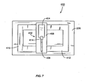
- Figure 7 illustrates a transponder 400 comprising an asymmetrical dipole antenna 402 coupled to a pair of asymmetrical loop antennas 410, 412. As illustrated in Figure 7, the dipole antenna 402 is positioned such that loop antenna 410 is smaller than loop antenna 412. Dipole antenna 402 comprises asymmetrical tabs 404, 406 as illustrated. Variations in the nature of the asymmetry to achieve the desired operating frequencies are considered within the skill of those in the industry. A further discussion of asymmetrical dipole antennas may be found in commonly owned U.S. patent application Serial No.
- a ground plane 408 is further used to tune the antennas 402, 410, 412.
- Chip 414 controls all the antennas 402, 410, 412. Further tuning may be achieved by varying the position of the various elements on the substrate 206. For example, some elements may be on one side, some embedded, and some on the other side; all the elements may be embedded; all the elements on one side; or other arrangement as needed or desired. It should be appreciated that the ground plane 408 may be isolated from the other elements to provide the desired grounding effect, but such may be done with a dielectric tape or the like as is well understood.
- this wireless communication device 400 has multi-frequency functionality in that the dipole antenna 402 may operate at a first frequency, the first loop antenna 410 may operate at a second frequency, and the second loop antenna 412 may operate at a third frequency.
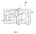
- Figure 8 illustrates a second variant wireless communication device 400A, wherein the ground plane 408A is slotted behind the dipole 402 to minimize interaction between the loop antennas 410, 412. This is a function of the fact that at UHF frequencies, the gap will appear as a high impedance gap. At the microwave frequencies of the dipole 402, the gap has a relatively low impedance and looks like a continuous ground plane, allowing the dipole 402 to operate normally.
- FIG. 9 illustrates a third variant with nested loops for improved bandwidth response.
- wireless communication device 450 comprises an asymmetrical dipole antenna 402, a ground plane 408, a first loop 412, a second loop 452, and a chip 414.
- Second loop 452 comprises a first part 454 and a second part 456, which are nested and coupled to the dipole 402. If the loops are similarly sized, but not identical, the overall circuit behaves like two coupled tuned circuits, giving an overall wider receive bandwidth than would be achieved with one loop.
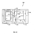
- FIG 10 illustrates a fourth variant wireless communication device 500.
- Wireless communication device 500 comprises a dipole antenna 402, a ground plane 408, a first loop antenna 412, and a second loop antenna 502.
- Second loop antenna 502 is electrically longer at low frequencies such as 13.56 MHz. Additionally, it should be noted that the coils of the second loop antenna 502 may be separated by a dielectric tape, or even by having an opposite surface connection.
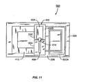
- FIG 11 illustrates a fifth variant wireless communication device 550.
- Wireless communication device 550 comprises a dipole antenna 402, a slotted ground plane 408B, a first loop antenna 412, and a second loop antenna 502A.
- the first loop antenna 412 is operative at UHF frequencies
- the dipole antenna 402 at microwave frequencies
- the second loop antenna 502A is operative at low frequencies akin to second loop antenna 502.
- the second loop antenna 502A is coupled to the chip 414 via capacitance between the two plates 552, 554 of the slotted ground plane 408B.
- a thin substrate 206 allows increases in the capacitive coupling between the dipole antenna 402 and the second loop antenna 502A.
- the narrow gap in the ground plane 408B is seen as a relatively low impedance gap at microwave frequencies, allowing the dipole antenna 402 to function normally.
- the variants and embodiments of Figures 6-11 are designed more from a fresh perspective than with an eye towards retrofitting. That does not mean that these variations may not be used in a retrofit context, but the presently commercially available wireless communication devices 200 are not designed to accommodate these variations as easily.
- the embodiments of Figures 6-11 are designed to operate with a single RFID chip, 256 or 414. Chip 256 or 414 can sense in a simple way which frequency at which the interrogation is occurring. If the chip 256, 414 has an input port connected to the antenna terminals prior to the internal rectifier, it will 'see' 13.56 MHz when being interrogated at this frequency, but not when being interrogated at higher frequencies.
- the interrogator 100 may simply send an identifier as part of the interrogation message.
- the identifier may identify the frequency at which the interrogator 100 is operating. This identifier may be in the form of amplitude modulation of the signal or other technique as desired.
- Figure 12 illustrates one type of tracking system whereby the transponder 130 attached to articles 161, for example, automobile 160, can be tracked through an environment such as a factory, distribution facility or storage facility.
- the transponder 130 connected to article 161 passes a first interrogation point 150 that includes an interrogation reader 100.
- a message containing information and/or a specific request for information may be transmitted by the interrogation reader 100 and received by the transponder 130.
- This process continues as the article 161 moves to a second interrogation point 152, a third interrogation point 154, a fourth interrogation point 156, and on to a last interrogation point 158.
- a central control system 159 maintains the information from interrogation readers 100 and monitors the movement of the articles 161 through the facility.
- the information received by each of the interrogation readers 100 may be forwarded to the central control system 159 in a variety of architectures such as parallel or serial communication or through use of a local area network (LAN) or wide area network (WAN).
- LAN local area network
- WAN wide area network
- Such architecture may include wiring between the interrogation readers 100 and the central control system 159 or may be wireless communication.
- the central control system 159 may also send information to the interrogation reader 100 to be transmitted back to the transponder 130 attached to the article 161 for a variety of purposes, including for identification.
- central control system 159 is designed to have knowledge of anticipated or expected whereabouts of the articles 161, then an alarm may be generated if the control system 159 expects to receive information about a particular article 161 and does not. Other situation based alarms may also be possible, such as when an item appears at the same station twice or if some other unexpected situation occurs.
- wireless communication devices 130 having their own transmission capability may still be used for tracking and communicating information concerning articles 161 without the use of interrogation readers 100.
- a receiver to receive communication from the wireless communication device 130 would be needed.
- multiple receivers may be used to triangulate the position of the tracked article 161.
- the system may need to have the ability to receive and transmit on different frequencies in order to distinguish wireless communication devices 130.
- an identification stored in memory 138 of the transponder 130 may also be used to distinguish wireless communication devices 130.
Claims (12)
- Dispositif de communication sans fil (130) comprenant : des circuits électroniques de communication (132) ; une première antenne à conducteur bouclé (202), ladite première antenne à conducteur bouclé (202) étant connectée de manière opérationnelle auxdits circuits électroniques de communication (132) ; une deuxième antenne à conducteur bouclé (204 ou 260), ladite deuxième antenne à conducteur bouclé (204 ou 260) étant connectée de manière opérationnelle auxdits circuits électroniques de communication (132) ; et une antenne à pôle (250), ladite antenne à pôle (250) étant connectée de manière opérationnelle auxdits circuits électroniques de communication (132), caractérisé en ce que
la première antenne à conducteur bouclé (202) fonctionne à une première fréquence, la deuxième antenne à conducteur bouclé (204 ou 260) fonctionne à une deuxième fréquence et l'antenne à pôle (250) fonctionne à une troisième fréquence, dans lequel lesdites fréquences sont différentes et lesdits circuits électroniques de communication (132) communiquent de manière sélective avec un interrogateur distant (100) par une desdites antennes (202, 204 ou 260, 250). - Dispositif de communication sans fil (130) selon la revendication 1, comprenant en outre une troisième antenne à conducteur bouclé (262) fonctionnant à une quatrième fréquence.
- Dispositif de communication sans fil (130) selon la revendication 2, dans lequel
ladite première antenne à conducteur bouclé (202), ladite deuxième antenne à conducteur bouclé (260) et ladite troisième antenne à conducteur bouclé (262) partagent un conducteur bouclé. - Dispositif de communication sans fil (130) selon la revendication 1, dans lequel
ladite antenne à pôle (250) comprend une antenne à dipôle et des deuxièmes circuits électroniques de communication (132, 256), lesdits premiers circuits électroniques de communication (132, 208) étant associés à une desdites antennes à conducteur bouclé (202, 204 ou 260) et lesdits deuxièmes circuits électroniques de communication (132, 256) étant associés à ladite antenne à dipôle (250). - Dispositif de communication sans fil selon la revendication 4, dans lequel
lesdits premiers circuits électroniques de communication sans fil (208) sont couplés à une antenne à conducteur bouclé (204) fonctionnant à la première fréquence, lesdits deuxièmes circuits électroniques de communication sans fil (256) sont couplés à travers ladite antenne à conducteur bouclé (204) et lesdits deuxièmes circuits électroniques de communication sans fil (256) se couplant à ladite antenne à conducteur bouclé (262), incluant lesdits premiers circuits électroniques de communication sans fil (208) à la deuxième fréquence de fonctionnement et se couplant à ladite antenne à conducteur bouclé (260) excluant lesdits circuits électroniques de communication sans fil (208) à une quatrième fréquence de fonctionnement. - Dispositif de communication sans fil selon la revendication 4, dans lequel
lesdits premiers circuits électroniques de communication sans fil (208) sont couplés à une antenne à conducteur bouclé (204) fonctionnant à 13,56 MHz, lesdits deuxièmes circuits électroniques de communication sans fil (256) sont couplés à travers ladite antenne à conducteur bouclé (204) et lesdits deuxièmes circuits électroniques de communication sans fil (256) se couplant à ladite antenne à conducteur bouclé (262), incluant lesdits premiers circuits électroniques de communication sans fil (208) à 868 MHz et se couplant à ladite antenne à conducteur bouclé (260) excluant lesdits circuits électroniques de communication sans fil (208) à 915 MHz et l'antenne à dipôle (250) fonctionne à 2,45 GHz. - Dispositif de communication sans fil (130) selon la revendication 1, dans lequel ladite antenne à pôle (250) est placée entre ladite première antenne à conducteur bouclé (202) et ladite deuxième antenne à conducteur bouclé (204 ou 260) et se couple de manière capacitive auxdites première et deuxième antennes à conducteur bouclé (202, 204 ou 260).
- Dispositif de communication sans fil (130) selon la revendication 1, dans lequel ladite antenne à pôle (250) est placée à travers lesdites première et deuxième antennes à conducteur bouclé (202, 204 ou 260).
- Procédé de poursuite d'un élément (161), comprenant : interroger un dispositif de communication sans fil (130) à une première fréquence par une première antenne à conducteur bouclé (202) sur le dispositif de communication sans fil ; interroger le dispositif de communication sans fil (130) à une deuxième fréquence par une antenne à dipôle (250) sur le dispositif de communication sans fil (130) ; caractérisé en ce que
le procédé comprend en outre interroger le dispositif de communication sans fil (130) à une troisième fréquence par une deuxième antenne à conducteur bouclé (204 ou 260) sur le dispositif de communication sans fil (130), dans lequel lesdites fréquences sont différentes. - Procédé selon la revendication 9, dans lequel interroger le dispositif de communication sans fil (130) à une deuxième fréquence par une antenne à dipôle (250) sur le dispositif de communication sans fil (130) comprend interroger le dispositif de communication sans fil (130) à une deuxième fréquence par une antenne à dipôle (250) couplée de manière capacitive auxdites première et deuxième antennes à conducteur bouclé (202, 204 ou 260).
- Procédé selon la revendication 9, dans lequel interroger le dispositif de communication sans fil (130) à une deuxième fréquence par une antenne à dipôle (250) sur le dispositif de communication sans fil (130) comprend interroger le dispositif de communication sans fil (130) à une deuxième fréquence par une antenne à dipôle (250) placée en travers desdites première et deuxième antennes à conducteur bouclé (202, 204 ou 260).
- Procédé selon la revendication 9, comprenant en outre interroger le dispositif de communication sans fil (130) à une quatrième fréquence par une troisième antenne à conducteur bouclé (262) sur le dispositif de communication sans fil (130).
Priority Applications (2)
| Application Number | Priority Date | Filing Date | Title |
|---|---|---|---|
| EP06006597.6A EP1689031B1 (fr) | 2000-10-03 | 2001-10-03 | Dispositif de communication mutlibande sans fil |
| EP06006596.8A EP1696512B1 (fr) | 2000-10-03 | 2001-10-03 | Dispositif de communication multibande sans fil. |
Applications Claiming Priority (3)
| Application Number | Priority Date | Filing Date | Title |
|---|---|---|---|
| US09/678,630 US6975834B1 (en) | 2000-10-03 | 2000-10-03 | Multi-band wireless communication device and method |
| US678630 | 2000-10-03 | ||
| PCT/GB2001/004399 WO2002029929A2 (fr) | 2000-10-03 | 2001-10-03 | Dispositif de communication sans fil multibande |
Related Child Applications (2)
| Application Number | Title | Priority Date | Filing Date |
|---|---|---|---|
| EP06006597.6A Division EP1689031B1 (fr) | 2000-10-03 | 2001-10-03 | Dispositif de communication mutlibande sans fil |
| EP06006596.8A Division EP1696512B1 (fr) | 2000-10-03 | 2001-10-03 | Dispositif de communication multibande sans fil. |
Publications (2)
| Publication Number | Publication Date |
|---|---|
| EP1323210A2 EP1323210A2 (fr) | 2003-07-02 |
| EP1323210B1 true EP1323210B1 (fr) | 2006-05-17 |
Family
ID=24723609
Family Applications (3)
| Application Number | Title | Priority Date | Filing Date |
|---|---|---|---|
| EP06006597.6A Expired - Lifetime EP1689031B1 (fr) | 2000-10-03 | 2001-10-03 | Dispositif de communication mutlibande sans fil |
| EP06006596.8A Expired - Lifetime EP1696512B1 (fr) | 2000-10-03 | 2001-10-03 | Dispositif de communication multibande sans fil. |
| EP01970038A Expired - Lifetime EP1323210B1 (fr) | 2000-10-03 | 2001-10-03 | Dispositif de communication sans fil multibande |
Family Applications Before (2)
| Application Number | Title | Priority Date | Filing Date |
|---|---|---|---|
| EP06006597.6A Expired - Lifetime EP1689031B1 (fr) | 2000-10-03 | 2001-10-03 | Dispositif de communication mutlibande sans fil |
| EP06006596.8A Expired - Lifetime EP1696512B1 (fr) | 2000-10-03 | 2001-10-03 | Dispositif de communication multibande sans fil. |
Country Status (7)
| Country | Link |
|---|---|
| US (4) | US6975834B1 (fr) |
| EP (3) | EP1689031B1 (fr) |
| JP (1) | JP2004511156A (fr) |
| AT (1) | ATE326778T1 (fr) |
| AU (1) | AU2001290157A1 (fr) |
| DE (1) | DE60119755T2 (fr) |
| WO (1) | WO2002029929A2 (fr) |
Cited By (1)
| Publication number | Priority date | Publication date | Assignee | Title |
|---|---|---|---|---|
| DE102007018097A1 (de) * | 2007-04-17 | 2008-11-13 | Infineon Technologies Austria Ag | Transponderschaltungsanordnung und Verfahren zum Betreiben eines Demodulators |
Families Citing this family (126)
| Publication number | Priority date | Publication date | Assignee | Title |
|---|---|---|---|---|
| US6975834B1 (en) | 2000-10-03 | 2005-12-13 | Mineral Lassen Llc | Multi-band wireless communication device and method |
| US20020183882A1 (en) | 2000-10-20 | 2002-12-05 | Michael Dearing | RF point of sale and delivery method and system using communication with remote computer and having features to read a large number of RF tags |
| US7258276B2 (en) | 2000-10-20 | 2007-08-21 | Promega Corporation | Radio frequency identification method and system of distributing products |
| USRE47599E1 (en) | 2000-10-20 | 2019-09-10 | Promega Corporation | RF point of sale and delivery method and system using communication with remote computer and having features to read a large number of RF tags |
| JP2004537906A (ja) | 2001-07-31 | 2004-12-16 | コーニンクレッカ フィリップス エレクトロニクス エヌ ヴィ | ゆるく結合されたアンテナ装置を有する通信局 |
| WO2003023900A1 (fr) | 2001-09-13 | 2003-03-20 | Fractus, S.A. | Plans de sol de couverture de l'espace a niveaux multiples pour antennes multibandes miniatures |
| AU2003233033A1 (en) | 2002-04-24 | 2003-11-10 | Marconi Intellectual Property (Us) Inc | Manufacturing method for a wireless communication device and manufacturing apparatus |
| JP2005531177A (ja) | 2002-06-25 | 2005-10-13 | フラクトゥス・ソシエダッド・アノニマ | ハンドヘルド端末装置用マルチバンドアンテナ |
| AU2003255949A1 (en) | 2002-07-09 | 2004-01-23 | Neology, Inc. | System and method for providing secure identification solutions |
| GB2393076A (en) * | 2002-09-12 | 2004-03-17 | Rf Tags Ltd | Radio frequency identification tag which has a ground plane not substantially larger than the area spanned by the patch antenna |
| JP3975918B2 (ja) * | 2002-09-27 | 2007-09-12 | ソニー株式会社 | アンテナ装置 |
| AU2003272940B2 (en) * | 2002-10-08 | 2008-08-07 | Nippon Carbide Kogyo Kabushiki Kaisha | Recursive-reflection display device |
| EP1563570A1 (fr) | 2002-11-07 | 2005-08-17 | Fractus, S.A. | Boitier de circuit integre incluant une antenne miniature |
| US6914562B2 (en) | 2003-04-10 | 2005-07-05 | Avery Dennison Corporation | RFID tag using a surface insensitive antenna structure |
| GB2402920A (en) * | 2003-06-21 | 2004-12-22 | Arjo Med Aktiebolag Ltd | Sling attachment device |
| US7317901B2 (en) * | 2004-02-09 | 2008-01-08 | Motorola, Inc. | Slotted multiple band antenna |
| FR2869707B1 (fr) * | 2004-04-29 | 2007-03-23 | Henri Havot | Antenne et etiquette electronique comprenant ladite antenne |
| KR100619695B1 (ko) * | 2004-06-23 | 2006-09-08 | 엘지전자 주식회사 | 안테나 및 이를 구비한 휴대용 단말기 |
| EP1771919A1 (fr) | 2004-07-23 | 2007-04-11 | Fractus, S.A. | Antenne dans un boitier a interaction electromagnetique reduite avec des elements integres sur la puce |
| DE102004038685A1 (de) * | 2004-08-10 | 2006-02-23 | Tkm Telekommunikation Und Elektronik Gmbh | Anordnung zur Identifikation und Lokalisation von Gegenständen |
| US7652632B2 (en) | 2004-08-18 | 2010-01-26 | Ruckus Wireless, Inc. | Multiband omnidirectional planar antenna apparatus with selectable elements |
| US7899497B2 (en) | 2004-08-18 | 2011-03-01 | Ruckus Wireless, Inc. | System and method for transmission parameter control for an antenna apparatus with selectable elements |
| US8031129B2 (en) | 2004-08-18 | 2011-10-04 | Ruckus Wireless, Inc. | Dual band dual polarization antenna array |
| US7933628B2 (en) | 2004-08-18 | 2011-04-26 | Ruckus Wireless, Inc. | Transmission and reception parameter control |
| US7880683B2 (en) | 2004-08-18 | 2011-02-01 | Ruckus Wireless, Inc. | Antennas with polarization diversity |
| US7965252B2 (en) | 2004-08-18 | 2011-06-21 | Ruckus Wireless, Inc. | Dual polarization antenna array with increased wireless coverage |
| US7193562B2 (en) | 2004-11-22 | 2007-03-20 | Ruckus Wireless, Inc. | Circuit board having a peripheral antenna apparatus with selectable antenna elements |
| US7696946B2 (en) | 2004-08-18 | 2010-04-13 | Ruckus Wireless, Inc. | Reducing stray capacitance in antenna element switching |
| US7362280B2 (en) * | 2004-08-18 | 2008-04-22 | Ruckus Wireless, Inc. | System and method for a minimized antenna apparatus with selectable elements |
| US7292198B2 (en) | 2004-08-18 | 2007-11-06 | Ruckus Wireless, Inc. | System and method for an omnidirectional planar antenna apparatus with selectable elements |
| EP1792363A1 (fr) | 2004-09-21 | 2007-06-06 | Fractus, S.A. | Plan de sol multiniveau pour un dispositif mobile |
| WO2006034940A1 (fr) | 2004-09-27 | 2006-04-06 | Fractus, S.A. | Antenne accordable |
| US7505447B2 (en) | 2004-11-05 | 2009-03-17 | Ruckus Wireless, Inc. | Systems and methods for improved data throughput in communications networks |
| US8638708B2 (en) | 2004-11-05 | 2014-01-28 | Ruckus Wireless, Inc. | MAC based mapping in IP based communications |
| US9240868B2 (en) | 2004-11-05 | 2016-01-19 | Ruckus Wireless, Inc. | Increasing reliable data throughput in a wireless network |
| US8619662B2 (en) | 2004-11-05 | 2013-12-31 | Ruckus Wireless, Inc. | Unicast to multicast conversion |
| EP1810368A1 (fr) | 2004-11-12 | 2007-07-25 | Fractus, S.A. | Structure d antenne pour un dispositif sans fil avec un plan de sol en forme de boucle |
| CN1934750B (zh) | 2004-11-22 | 2012-07-18 | 鲁库斯无线公司 | 包括具有可选择天线元件的外围天线装置的电路板 |
| US7358912B1 (en) | 2005-06-24 | 2008-04-15 | Ruckus Wireless, Inc. | Coverage antenna apparatus with selectable horizontal and vertical polarization elements |
| US8792414B2 (en) | 2005-07-26 | 2014-07-29 | Ruckus Wireless, Inc. | Coverage enhancement using dynamic antennas |
| WO2006070017A1 (fr) | 2004-12-30 | 2006-07-06 | Fractus, S.A. | Antenne a plan de sol pour un appareil de radio |
| US7893882B2 (en) | 2007-01-08 | 2011-02-22 | Ruckus Wireless, Inc. | Pattern shaping of RF emission patterns |
| US7646343B2 (en) | 2005-06-24 | 2010-01-12 | Ruckus Wireless, Inc. | Multiple-input multiple-output wireless antennas |
| US7545272B2 (en) | 2005-02-08 | 2009-06-09 | Therasense, Inc. | RF tag on test strips, test strip vials and boxes |
| US7385561B2 (en) * | 2005-02-17 | 2008-06-10 | Galtronics Ltd. | Multiple monopole antenna |
| EP1859508A1 (fr) | 2005-03-15 | 2007-11-28 | Fractus, S.A. | Plan de masse a fente utilise comme antenne a fente ou pour une antenne pifa |
| WO2006097918A2 (fr) | 2005-03-15 | 2006-09-21 | Galtronics Ltd. | Antenne a alimentation capacitive |
| JP2006295729A (ja) * | 2005-04-13 | 2006-10-26 | Fujitsu Ltd | Rfidタグおよびアンテナ配置方法 |
| EP1724711A1 (fr) * | 2005-05-11 | 2006-11-22 | Axalto SA | Système pour positionner un document électronique à l'antenne d'un lecteur sans contact |
| EP1911124A1 (fr) | 2005-07-21 | 2008-04-16 | Fractus, S.A. | Dispositif portatif avec deux antennes et procédé d'amélioration de l'isolement entre les antennes |
| FR2888973B1 (fr) * | 2005-07-22 | 2007-10-26 | K Sa As | Dispositif de lecture optique et d'encodage radiofrequence adaptable en sortie d'imprimante d'etiquettes d'identification |
| WO2007017944A1 (fr) * | 2005-08-10 | 2007-02-15 | Hitachi, Ltd. | Antenne |
| US20070057795A1 (en) * | 2005-09-12 | 2007-03-15 | Wakahiro Kawai | Inspection method of RFID tag |
| US20070115762A1 (en) * | 2005-11-21 | 2007-05-24 | Wisnudel Marc B | Optical article having anti-theft feature and a system and method for inhibiting theft of same |
| CN101322346A (zh) | 2005-12-01 | 2008-12-10 | 鲁库斯无线公司 | 借助于无线基站虚拟化的按需服务 |
| US7750813B2 (en) * | 2005-12-14 | 2010-07-06 | University Of Kansas | Microstrip antenna for RFID device |
| US8564439B2 (en) | 2010-05-27 | 2013-10-22 | The University Of Kansas | Microstrip antenna for RFID device |
| US9071583B2 (en) | 2006-04-24 | 2015-06-30 | Ruckus Wireless, Inc. | Provisioned configuration for automatic wireless connection |
| US7788703B2 (en) | 2006-04-24 | 2010-08-31 | Ruckus Wireless, Inc. | Dynamic authentication in secured wireless networks |
| US9769655B2 (en) | 2006-04-24 | 2017-09-19 | Ruckus Wireless, Inc. | Sharing security keys with headless devices |
| FR2901041B1 (fr) * | 2006-05-12 | 2008-10-10 | Eric Heurtier | Etiquette integrant une antenne anti-vol rf et un transporteur rfid uhf |
| US7954722B2 (en) | 2006-05-30 | 2011-06-07 | Hitachi, Ltd. | IC tag and inlet for IC tag |
| JP4681506B2 (ja) | 2006-05-30 | 2011-05-11 | 株式会社日立製作所 | Icタグ |
| DE102006028827A1 (de) * | 2006-06-21 | 2008-01-10 | Dynamic Systems Gmbh | Transponder mit elektronischem Speicherchip und magnetischer Ringantenne |
| US8670725B2 (en) | 2006-08-18 | 2014-03-11 | Ruckus Wireless, Inc. | Closed-loop automatic channel selection |
| US8165552B2 (en) * | 2006-09-29 | 2012-04-24 | Broadcom Corporation | Method and system for identifying radio frequency identification (RFID) tag location using a switchable coil |
| US8031651B2 (en) | 2006-09-29 | 2011-10-04 | Broadcom Corporation | Method and system for minimizing power consumption in a communication system |
| US20080079587A1 (en) * | 2006-09-29 | 2008-04-03 | Ahmadreza Rofougaran | Method And System For Utilizing Magnetic On-Chip Coil For Ultra High Frequency (UHF) |
| US8026818B2 (en) | 2006-12-20 | 2011-09-27 | Checkpoint Systems, Inc. | EAS and UHF combination tag |
| WO2008090943A1 (fr) * | 2007-01-26 | 2008-07-31 | Murata Manufacturing Co., Ltd. | Conteneur avec module à couplage électromagnétique |
| JP5076519B2 (ja) | 2007-01-31 | 2012-11-21 | 富士通株式会社 | タグ |
| US7710275B2 (en) | 2007-03-16 | 2010-05-04 | Promega Corporation | RFID reader enclosure and man-o-war RFID reader system |
| JP2008250573A (ja) * | 2007-03-29 | 2008-10-16 | Brother Ind Ltd | アンテナ装置及び無線タグ通信装置 |
| US8009101B2 (en) * | 2007-04-06 | 2011-08-30 | Murata Manufacturing Co., Ltd. | Wireless IC device |
| FR2915822A1 (fr) * | 2007-05-03 | 2008-11-07 | Pygmalyon Sa | Etiquette resonnante et passive de detection ou d'identification radiofrequence |
| DE102007029083B4 (de) | 2007-06-21 | 2019-05-16 | ASTRA Gesellschaft für Asset Management mbH & Co. KG | Kartendatenträger mit Detektierplättchen |
| US7768407B2 (en) | 2007-06-22 | 2010-08-03 | Avery Dennison Corporation | Foldable RFID device interposer and method |
| EP2169767A4 (fr) * | 2007-07-18 | 2011-01-05 | Fujitsu Ltd | Marqueur sans fil et procédé de fabrication du marqueur sans fil |
| TWI381577B (zh) * | 2007-07-18 | 2013-01-01 | Fujitsu Ltd | 無線射頻識別標籤及無線射頻識別標籤之製造方法 |
| US8547899B2 (en) | 2007-07-28 | 2013-10-01 | Ruckus Wireless, Inc. | Wireless network throughput enhancement through channel aware scheduling |
| AU2008296060B2 (en) * | 2007-09-06 | 2014-06-05 | Deka Products Limited Partnership | RFID system and method |
| US7880614B2 (en) * | 2007-09-26 | 2011-02-01 | Avery Dennison Corporation | RFID interposer with impedance matching |
| DE102008056926A1 (de) * | 2007-11-19 | 2009-12-24 | Brühn, Xenia | Drahtlose passive Tastaturfunktion |
| US8633821B2 (en) * | 2007-12-03 | 2014-01-21 | Avery Dennison Corporation | Dual use RFID/EAS device |
| US8847764B2 (en) * | 2007-12-05 | 2014-09-30 | Avery Dennison Corporation | RFID system with distributed read structure |
| US7786868B2 (en) * | 2007-12-11 | 2010-08-31 | Avery Dennison Corporation | RFID device with multiple passive operation modes |
| JP5188167B2 (ja) | 2007-12-20 | 2013-04-24 | 株式会社ユニバーサルエンターテインメント | 紙葉類処理装置 |
| US8355343B2 (en) | 2008-01-11 | 2013-01-15 | Ruckus Wireless, Inc. | Determining associations in a mesh network |
| DE102008024825A1 (de) * | 2008-05-23 | 2009-12-03 | Smartrac Ip B.V. | Antennenanordnung für die Chipkartenherstellung |
| TWI375351B (en) * | 2008-07-15 | 2012-10-21 | Wistron Neweb Corp | An antenna and an electronic device having the antenna |
| CN103647156B (zh) * | 2008-07-17 | 2015-10-14 | 高通股份有限公司 | 高频无线功率发射天线的自适应匹配和调谐 |
| US8740266B2 (en) | 2008-07-18 | 2014-06-03 | Patrick E. Keller | Sentinel event reducing safety knobs |
| US20100045559A1 (en) * | 2008-08-25 | 2010-02-25 | Vivant Medical, Inc. | Dual-Band Dipole Microwave Ablation Antenna |
| EP2351150A1 (fr) * | 2008-11-05 | 2011-08-03 | TomTom International B.V. | Appareil station d'accueil |
| US8217843B2 (en) | 2009-03-13 | 2012-07-10 | Ruckus Wireless, Inc. | Adjustment of radiation patterns utilizing a position sensor |
| US8698675B2 (en) | 2009-05-12 | 2014-04-15 | Ruckus Wireless, Inc. | Mountable antenna elements for dual band antenna |
| US20110090060A1 (en) * | 2009-10-16 | 2011-04-21 | Tavshikar Milind M | Isolating RFID Reader |
| EP2350863B1 (fr) | 2009-11-16 | 2015-08-26 | Ruckus Wireless, Inc. | Création d'un réseau maillé avec des liaisons câblées et sans fil |
| US9979626B2 (en) | 2009-11-16 | 2018-05-22 | Ruckus Wireless, Inc. | Establishing a mesh network with wired and wireless links |
| US8228251B1 (en) | 2010-08-23 | 2012-07-24 | University Of Central Florida Research Foundation, Inc. | Ultra-wideband, low profile antenna |
| US9407012B2 (en) | 2010-09-21 | 2016-08-02 | Ruckus Wireless, Inc. | Antenna with dual polarization and mountable antenna elements |
| US9792188B2 (en) | 2011-05-01 | 2017-10-17 | Ruckus Wireless, Inc. | Remote cable access point reset |
| WO2013095458A1 (fr) * | 2011-12-21 | 2013-06-27 | Intel Corporation | Antenne à cadre dissymétrique pour faciliter un couplage de champ proche |
| US8798536B2 (en) | 2012-01-27 | 2014-08-05 | Blackberry Limited | Mobile wireless communications device including parallel NFC loop antennas and associated methods |
| US8756668B2 (en) | 2012-02-09 | 2014-06-17 | Ruckus Wireless, Inc. | Dynamic PSK for hotspots |
| US10186750B2 (en) | 2012-02-14 | 2019-01-22 | Arris Enterprises Llc | Radio frequency antenna array with spacing element |
| US9634403B2 (en) | 2012-02-14 | 2017-04-25 | Ruckus Wireless, Inc. | Radio frequency emission pattern shaping |
| US9092610B2 (en) | 2012-04-04 | 2015-07-28 | Ruckus Wireless, Inc. | Key assignment for a brand |
| EP2839536A1 (fr) * | 2012-04-19 | 2015-02-25 | Smartrac IP B.V. | Structure de boucle intégrée pour identification par radiofréquence |
| EP2867996B1 (fr) * | 2012-06-28 | 2019-08-07 | Teknologian tutkimuskeskus VTT Oy | Système d'identification uhf en champ proche et procédé d'identification d'un objet ou du type d'un objet qui est ou qui contient un matériau électriquement conducteur utilisant une identification en champ proche |
| US9570799B2 (en) | 2012-09-07 | 2017-02-14 | Ruckus Wireless, Inc. | Multiband monopole antenna apparatus with ground plane aperture |
| WO2014146038A1 (fr) | 2013-03-15 | 2014-09-18 | Ruckus Wireless, Inc. | Réflecteur à faible bande pour une antenne directionnelle à double bande |
| US9431712B2 (en) | 2013-05-22 | 2016-08-30 | Wisconsin Alumni Research Foundation | Electrically-small, low-profile, ultra-wideband antenna |
| US9621230B2 (en) * | 2014-03-03 | 2017-04-11 | Apple Inc. | Electronic device with near-field antennas |
| US9337540B2 (en) | 2014-06-04 | 2016-05-10 | Wisconsin Alumni Research Foundation | Ultra-wideband, low profile antenna |
| US20160064807A1 (en) * | 2014-08-29 | 2016-03-03 | Laird Technologies, Inc. | Multiband Vehicular Antenna Assemblies |
| US10438110B2 (en) | 2015-07-08 | 2019-10-08 | Assa Abloy Ab | Multiple frequency transponder with a single antenna |
| US20170162952A1 (en) * | 2015-12-03 | 2017-06-08 | Checkpoint Systems, Inc. | Multi-loop antenna |
| CN107437648B (zh) * | 2016-05-28 | 2021-04-20 | 富泰华工业(深圳)有限公司 | 多馈入超高频rfid标签天线 |
| BR112020021426A2 (pt) * | 2018-04-20 | 2021-01-19 | Avery Dennison Retail Information Services, Llc | Correias de rfid com um condutor superior e inferior |
| US10978791B2 (en) | 2018-05-07 | 2021-04-13 | Nxp B.V. | Combination antenna |
| TWI731269B (zh) * | 2018-10-02 | 2021-06-21 | 緯創資通股份有限公司 | 天線系統 |
| EP3839826B1 (fr) * | 2019-12-20 | 2022-08-10 | Assa Abloy AB | Ensemble rfid |
| US20210330190A1 (en) * | 2020-04-22 | 2021-10-28 | Biotags, LLC | Temperature sensor patch and system |
| JP2021196931A (ja) * | 2020-06-16 | 2021-12-27 | 株式会社デンソーウェーブ | 干渉抑制機器及び干渉抑制システム |
| WO2023156922A1 (fr) * | 2022-02-17 | 2023-08-24 | Avery Dennison Retail Information Services Llc | Antenne rfid double |
Family Cites Families (49)
| Publication number | Priority date | Publication date | Assignee | Title |
|---|---|---|---|---|
| NO126975B (fr) * | 1967-03-30 | 1973-04-16 | John Welsh | |
| US3721990A (en) * | 1971-12-27 | 1973-03-20 | Rca Corp | Physically small combined loop and dipole all channel television antenna system |
| US4433336A (en) | 1982-02-05 | 1984-02-21 | The United States Of America As Represented By The Secretary Of Commerce | Three-element antenna formed of orthogonal loops mounted on a monopole |
| US4468674A (en) * | 1982-07-22 | 1984-08-28 | Blonder-Tongue Laboratories, Inc. | Assymetrical folded half-dipole and linear extension antenna array |
| SE450057B (sv) | 1984-11-20 | 1987-06-01 | Saab Automation Ab | Identitetsbrickor for identifiering av foremal |
| US4727598A (en) * | 1985-07-15 | 1988-02-23 | General Electric Company | Selectively mountable TV receiver cabinet and antenna |
| US4857893A (en) | 1986-07-18 | 1989-08-15 | Bi Inc. | Single chip transponder device |
| US5198826A (en) * | 1989-09-22 | 1993-03-30 | Nippon Sheet Glass Co., Ltd. | Wide-band loop antenna with outer and inner loop conductors |
| US5182570A (en) * | 1989-11-13 | 1993-01-26 | X-Cyte Inc. | End fed flat antenna |
| US5572226A (en) | 1992-05-15 | 1996-11-05 | Micron Technology, Inc. | Spherical antenna pattern(s) from antenna(s) arranged in a two-dimensional plane for use in RFID tags and labels |
| US6045652A (en) | 1992-06-17 | 2000-04-04 | Micron Communications, Inc. | Method of manufacturing an enclosed transceiver |
| DE4345610B4 (de) * | 1992-06-17 | 2013-01-03 | Micron Technology Inc. | Verfahren zur Herstellung einer Hochfrequenz-Identifikationseinrichtung (HFID) |
| US5779839A (en) | 1992-06-17 | 1998-07-14 | Micron Communications, Inc. | Method of manufacturing an enclosed transceiver |
| US5776278A (en) * | 1992-06-17 | 1998-07-07 | Micron Communications, Inc. | Method of manufacturing an enclosed transceiver |
| JPH06175264A (ja) | 1992-12-03 | 1994-06-24 | Konica Corp | ハロゲン化銀写真感光材料 |
| ZA941671B (en) | 1993-03-11 | 1994-10-12 | Csir | Attaching an electronic circuit to a substrate. |
| US5585953A (en) | 1993-08-13 | 1996-12-17 | Gec Plessey Semiconductors, Inc. | IR/RF radio transceiver and method |
| JPH0844831A (ja) | 1994-07-27 | 1996-02-16 | Nippon Telegr & Teleph Corp <Ntt> | ハイブリッドカードとそれを使用した無線通信システム |
| US5528222A (en) * | 1994-09-09 | 1996-06-18 | International Business Machines Corporation | Radio frequency circuit and memory in thin flexible package |
| US5682143A (en) | 1994-09-09 | 1997-10-28 | International Business Machines Corporation | Radio frequency identification tag |
| US5952977A (en) * | 1994-11-04 | 1999-09-14 | Mazda Motor Corporation | Glass antenna |
| JP3337865B2 (ja) | 1995-04-22 | 2002-10-28 | ソニーケミカル株式会社 | 合成ループアンテナ |
| US5592182A (en) | 1995-07-10 | 1997-01-07 | Texas Instruments Incorporated | Efficient, dual-polarization, three-dimensionally omni-directional crossed-loop antenna with a planar base element |
| JPH09260925A (ja) | 1996-03-19 | 1997-10-03 | Matsushita Electric Ind Co Ltd | アンテナ装置 |
| US6027027A (en) | 1996-05-31 | 2000-02-22 | Lucent Technologies Inc. | Luggage tag assembly |
| US5995048A (en) | 1996-05-31 | 1999-11-30 | Lucent Technologies Inc. | Quarter wave patch antenna |
| BR9808620A (pt) * | 1997-03-10 | 2000-05-16 | Precision Dynamics Corp | Elementos reativamente acoplados em circuitos sobre substratos flexìveis |
| JP3646908B2 (ja) | 1997-03-17 | 2005-05-11 | 株式会社吉野工業所 | 液体噴出器の押下げヘッド |
| US6094173A (en) | 1997-04-18 | 2000-07-25 | Motorola, Inc. | Method and apparatus for detecting an RFID tag signal |
| US5972152A (en) | 1997-05-16 | 1999-10-26 | Micron Communications, Inc. | Methods of fixturing flexible circuit substrates and a processing carrier, processing a flexible circuit and processing a flexible circuit substrate relative to a processing carrier |
| WO1999008402A1 (fr) | 1997-08-08 | 1999-02-18 | Micron Communications, Inc. | Systeme de communication sans fil comprenant plusieurs antennes commutables et procede de communication sans fil |
| AU761995B2 (en) | 1997-09-11 | 2003-06-12 | Precision Dynamics Corporation | Laminated radio frequency identification device |
| US6089458A (en) | 1997-10-17 | 2000-07-18 | Micron Technology, Inc. | Method of processing liquids, epoxy fabrication method, method of fabricating a radio frequency intelligent communication device, and method involving a mixture of different liquids |
| US5929760A (en) | 1997-10-20 | 1999-07-27 | Escort Memory Systems | RFID conveyor antenna |
| US5929813A (en) | 1998-01-09 | 1999-07-27 | Nokia Mobile Phones Limited | Antenna for mobile communications device |
| AU2576999A (en) | 1998-02-26 | 1999-09-15 | Intermec Ip Corp. | Multifunction antenna mounting for a communications instrument, such as a symbolreader |
| US6075973A (en) * | 1998-05-18 | 2000-06-13 | Micron Technology, Inc. | Method of communications in a backscatter system, interrogator, and backscatter communications system |
| FR2779235B1 (fr) * | 1998-05-26 | 2002-11-29 | Applic Rech Electronique | Systeme d'antennes de radiogoniometrie |
| US6154137A (en) * | 1998-06-08 | 2000-11-28 | 3M Innovative Properties Company | Identification tag with enhanced security |
| AU4715999A (en) * | 1998-06-24 | 2000-01-10 | Pinpoint Corporation | Dual mode tracking system |
| CA2276729A1 (fr) * | 1998-07-10 | 2000-01-10 | Albert Henry Kent | Laine minerale defibree et son mode d'obtention |
| JP2000077928A (ja) | 1998-09-03 | 2000-03-14 | Lintec Corp | ループアンテナ及びデータキャリア |
| US6100804A (en) | 1998-10-29 | 2000-08-08 | Intecmec Ip Corp. | Radio frequency identification system |
| EP1026779A3 (fr) * | 1999-02-01 | 2003-06-04 | Supersensor (Proprietary) Limited | Agencement d'antenne hybride utilisé pour des systèmes d'identifications électroniques |
| US6043746A (en) | 1999-02-17 | 2000-03-28 | Microchip Technology Incorporated | Radio frequency identification (RFID) security tag for merchandise and method therefor |
| EP1734461A2 (fr) * | 1999-07-12 | 2006-12-20 | Matsushita Electric Industrial Co., Ltd. | Appareil de distinction de corps mobile pour acquérir rapidement des jeux de données respectifs transmis par la modulation d'ondes radio réfléchies par des transpondeurs disposés à l'intérieur d'une zone de communication d'un appareil interrogateur |
| US6868073B1 (en) * | 2000-06-06 | 2005-03-15 | Battelle Memorial Institute K1-53 | Distance/ranging by determination of RF phase delta |
| US6639541B1 (en) * | 2000-08-29 | 2003-10-28 | The United States Of America As Represented By The Secretary Of The Navy | Device and method for detecting, measuring, and reporting low-level interference at a receiver |
| US6975834B1 (en) | 2000-10-03 | 2005-12-13 | Mineral Lassen Llc | Multi-band wireless communication device and method |
-
2000
- 2000-10-03 US US09/678,630 patent/US6975834B1/en not_active Expired - Lifetime
-
2001
- 2001-10-03 WO PCT/GB2001/004399 patent/WO2002029929A2/fr active IP Right Grant
- 2001-10-03 EP EP06006597.6A patent/EP1689031B1/fr not_active Expired - Lifetime
- 2001-10-03 AU AU2001290157A patent/AU2001290157A1/en not_active Abandoned
- 2001-10-03 JP JP2002533433A patent/JP2004511156A/ja active Pending
- 2001-10-03 EP EP06006596.8A patent/EP1696512B1/fr not_active Expired - Lifetime
- 2001-10-03 AT AT01970038T patent/ATE326778T1/de not_active IP Right Cessation
- 2001-10-03 DE DE60119755T patent/DE60119755T2/de not_active Expired - Lifetime
- 2001-10-03 EP EP01970038A patent/EP1323210B1/fr not_active Expired - Lifetime
-
2005
- 2005-12-12 US US11/302,416 patent/US7623834B2/en not_active Expired - Fee Related
-
2006
- 2006-08-31 US US11/514,436 patent/US7623835B2/en not_active Expired - Fee Related
-
2009
- 2009-02-25 US US12/392,986 patent/US7899425B2/en not_active Expired - Fee Related
Cited By (1)
| Publication number | Priority date | Publication date | Assignee | Title |
|---|---|---|---|---|
| DE102007018097A1 (de) * | 2007-04-17 | 2008-11-13 | Infineon Technologies Austria Ag | Transponderschaltungsanordnung und Verfahren zum Betreiben eines Demodulators |
Also Published As
| Publication number | Publication date |
|---|---|
| US7623835B2 (en) | 2009-11-24 |
| AU2001290157A1 (en) | 2002-04-15 |
| US20060160513A1 (en) | 2006-07-20 |
| US20060293014A1 (en) | 2006-12-28 |
| DE60119755T2 (de) | 2007-05-03 |
| JP2004511156A (ja) | 2004-04-08 |
| WO2002029929A2 (fr) | 2002-04-11 |
| EP1689031B1 (fr) | 2016-08-10 |
| WO2002029929A3 (fr) | 2002-07-18 |
| US7623834B2 (en) | 2009-11-24 |
| US6975834B1 (en) | 2005-12-13 |
| ATE326778T1 (de) | 2006-06-15 |
| US20090153303A1 (en) | 2009-06-18 |
| EP1689031A2 (fr) | 2006-08-09 |
| EP1696512A3 (fr) | 2007-01-10 |
| EP1696512A2 (fr) | 2006-08-30 |
| EP1689031A3 (fr) | 2007-05-23 |
| EP1696512B1 (fr) | 2016-06-15 |
| DE60119755D1 (de) | 2006-06-22 |
| EP1323210A2 (fr) | 2003-07-02 |
| US7899425B2 (en) | 2011-03-01 |
Similar Documents
| Publication | Publication Date | Title |
|---|---|---|
| EP1323210B1 (fr) | Dispositif de communication sans fil multibande | |
| EP1269395B1 (fr) | Dispositif d'identification de contenant | |
| US7336243B2 (en) | Radio frequency identification tag | |
| US7262701B1 (en) | Antenna structures for RFID devices | |
| US7800503B2 (en) | Radio frequency identification (RFID) tag antenna design | |
| US7075435B2 (en) | RFID tag assembly and system | |
| US9911017B2 (en) | Integrated RFID antenna fabrication method and apparatus for transponder assembly | |
| US6584301B1 (en) | Inductive reader device and method with integrated antenna and signal coupler | |
| AU2001283216A1 (en) | Rfid tag assembly and system | |
| MXPA04010053A (es) | Circuito integrado con acoplamiento mejorado. | |
| EP1472642A1 (fr) | Antenne d'amelioration destinee a une identification d'article | |
| US20140203989A1 (en) | High frequency (hf)/ultra high frequency (uhf) radio frequency identification (rfid) dual-band tag antenna | |
| CN102576927B (zh) | 例如用于rfid应答器系统的天线结构 | |
| KR100820544B1 (ko) | Rfid 태그 및 그 안테나 | |
| JP2005323019A (ja) | Rfidタグ用ブースターアンテナ | |
| CN103004015A (zh) | 天线配置方法和装置 | |
| US11551017B2 (en) | RFID system with improved signal transmission characteristics | |
| KR20110022895A (ko) | Tcp/ip기반 rfid 멀티 리더기 |
Legal Events
| Date | Code | Title | Description |
|---|---|---|---|
| PUAI | Public reference made under article 153(3) epc to a published international application that has entered the european phase |
Free format text: ORIGINAL CODE: 0009012 |
|
| 17P | Request for examination filed |
Effective date: 20030423 |
|
| AK | Designated contracting states |
Designated state(s): AT BE CH CY DE DK ES FI FR GB GR IE IT LI LU MC NL PT SE TR |
|
| AX | Request for extension of the european patent |
Extension state: AL LT LV MK RO SI |
|
| RAP1 | Party data changed (applicant data changed or rights of an application transferred) |
Owner name: MARCONI INTELLECTUAL PROPERTY (US) INC. |
|
| 17Q | First examination report despatched |
Effective date: 20041109 |
|
| RAP1 | Party data changed (applicant data changed or rights of an application transferred) |
Owner name: MINERAL LASSEN LLC |
|
| GRAP | Despatch of communication of intention to grant a patent |
Free format text: ORIGINAL CODE: EPIDOSNIGR1 |
|
| GRAS | Grant fee paid |
Free format text: ORIGINAL CODE: EPIDOSNIGR3 |
|
| GRAA | (expected) grant |
Free format text: ORIGINAL CODE: 0009210 |
|
| AK | Designated contracting states |
Kind code of ref document: B1 Designated state(s): AT BE CH CY DE DK ES FI FR GB GR IE IT LI LU MC NL PT SE TR |
|
| PG25 | Lapsed in a contracting state [announced via postgrant information from national office to epo] |
Ref country code: AT Free format text: LAPSE BECAUSE OF FAILURE TO SUBMIT A TRANSLATION OF THE DESCRIPTION OR TO PAY THE FEE WITHIN THE PRESCRIBED TIME-LIMIT Effective date: 20060517 Ref country code: LI Free format text: LAPSE BECAUSE OF FAILURE TO SUBMIT A TRANSLATION OF THE DESCRIPTION OR TO PAY THE FEE WITHIN THE PRESCRIBED TIME-LIMIT Effective date: 20060517 Ref country code: CH Free format text: LAPSE BECAUSE OF FAILURE TO SUBMIT A TRANSLATION OF THE DESCRIPTION OR TO PAY THE FEE WITHIN THE PRESCRIBED TIME-LIMIT Effective date: 20060517 Ref country code: BE Free format text: LAPSE BECAUSE OF FAILURE TO SUBMIT A TRANSLATION OF THE DESCRIPTION OR TO PAY THE FEE WITHIN THE PRESCRIBED TIME-LIMIT Effective date: 20060517 Ref country code: IT Free format text: LAPSE BECAUSE OF FAILURE TO SUBMIT A TRANSLATION OF THE DESCRIPTION OR TO PAY THE FEE WITHIN THE PRESCRIBED TIME-LIMIT;WARNING: LAPSES OF ITALIAN PATENTS WITH EFFECTIVE DATE BEFORE 2007 MAY HAVE OCCURRED AT ANY TIME BEFORE 2007. THE CORRECT EFFECTIVE DATE MAY BE DIFFERENT FROM THE ONE RECORDED. Effective date: 20060517 Ref country code: NL Free format text: LAPSE BECAUSE OF FAILURE TO SUBMIT A TRANSLATION OF THE DESCRIPTION OR TO PAY THE FEE WITHIN THE PRESCRIBED TIME-LIMIT Effective date: 20060517 Ref country code: FI Free format text: LAPSE BECAUSE OF FAILURE TO SUBMIT A TRANSLATION OF THE DESCRIPTION OR TO PAY THE FEE WITHIN THE PRESCRIBED TIME-LIMIT Effective date: 20060517 |
|
| REG | Reference to a national code |
Ref country code: GB Ref legal event code: FG4D |
|
| REG | Reference to a national code |
Ref country code: CH Ref legal event code: EP |
|
| REG | Reference to a national code |
Ref country code: IE Ref legal event code: FG4D |
|
| REF | Corresponds to: |
Ref document number: 60119755 Country of ref document: DE Date of ref document: 20060622 Kind code of ref document: P |
|
| PG25 | Lapsed in a contracting state [announced via postgrant information from national office to epo] |
Ref country code: DK Free format text: LAPSE BECAUSE OF FAILURE TO SUBMIT A TRANSLATION OF THE DESCRIPTION OR TO PAY THE FEE WITHIN THE PRESCRIBED TIME-LIMIT Effective date: 20060817 Ref country code: SE Free format text: LAPSE BECAUSE OF FAILURE TO SUBMIT A TRANSLATION OF THE DESCRIPTION OR TO PAY THE FEE WITHIN THE PRESCRIBED TIME-LIMIT Effective date: 20060817 |
|
| PG25 | Lapsed in a contracting state [announced via postgrant information from national office to epo] |
Ref country code: ES Free format text: LAPSE BECAUSE OF FAILURE TO SUBMIT A TRANSLATION OF THE DESCRIPTION OR TO PAY THE FEE WITHIN THE PRESCRIBED TIME-LIMIT Effective date: 20060828 |
|
| PG25 | Lapsed in a contracting state [announced via postgrant information from national office to epo] |
Ref country code: IE Free format text: LAPSE BECAUSE OF NON-PAYMENT OF DUE FEES Effective date: 20061003 |
|
| PG25 | Lapsed in a contracting state [announced via postgrant information from national office to epo] |
Ref country code: PT Free format text: LAPSE BECAUSE OF FAILURE TO SUBMIT A TRANSLATION OF THE DESCRIPTION OR TO PAY THE FEE WITHIN THE PRESCRIBED TIME-LIMIT Effective date: 20061017 |
|
| PG25 | Lapsed in a contracting state [announced via postgrant information from national office to epo] |
Ref country code: MC Free format text: LAPSE BECAUSE OF NON-PAYMENT OF DUE FEES Effective date: 20061031 |
|
| NLV1 | Nl: lapsed or annulled due to failure to fulfill the requirements of art. 29p and 29m of the patents act | ||
| REG | Reference to a national code |
Ref country code: CH Ref legal event code: PL |
|
| ET | Fr: translation filed | ||
| PLBE | No opposition filed within time limit |
Free format text: ORIGINAL CODE: 0009261 |
|
| STAA | Information on the status of an ep patent application or granted ep patent |
Free format text: STATUS: NO OPPOSITION FILED WITHIN TIME LIMIT |
|
| 26N | No opposition filed |
Effective date: 20070220 |
|
| PG25 | Lapsed in a contracting state [announced via postgrant information from national office to epo] |
Ref country code: GR Free format text: LAPSE BECAUSE OF FAILURE TO SUBMIT A TRANSLATION OF THE DESCRIPTION OR TO PAY THE FEE WITHIN THE PRESCRIBED TIME-LIMIT Effective date: 20060818 |
|
| PG25 | Lapsed in a contracting state [announced via postgrant information from national office to epo] |
Ref country code: TR Free format text: LAPSE BECAUSE OF FAILURE TO SUBMIT A TRANSLATION OF THE DESCRIPTION OR TO PAY THE FEE WITHIN THE PRESCRIBED TIME-LIMIT Effective date: 20060517 Ref country code: LU Free format text: LAPSE BECAUSE OF NON-PAYMENT OF DUE FEES Effective date: 20061003 |
|
| PG25 | Lapsed in a contracting state [announced via postgrant information from national office to epo] |
Ref country code: CY Free format text: LAPSE BECAUSE OF FAILURE TO SUBMIT A TRANSLATION OF THE DESCRIPTION OR TO PAY THE FEE WITHIN THE PRESCRIBED TIME-LIMIT Effective date: 20060517 |
|
| PGFP | Annual fee paid to national office [announced via postgrant information from national office to epo] |
Ref country code: DE Payment date: 20121031 Year of fee payment: 12 |
|
| REG | Reference to a national code |
Ref country code: DE Ref legal event code: R119 Ref document number: 60119755 Country of ref document: DE Effective date: 20140501 |
|
| PG25 | Lapsed in a contracting state [announced via postgrant information from national office to epo] |
Ref country code: DE Free format text: LAPSE BECAUSE OF NON-PAYMENT OF DUE FEES Effective date: 20140501 |
|
| REG | Reference to a national code |
Ref country code: FR Ref legal event code: PLFP Year of fee payment: 16 |
|
| REG | Reference to a national code |
Ref country code: FR Ref legal event code: PLFP Year of fee payment: 17 |
|
| PGFP | Annual fee paid to national office [announced via postgrant information from national office to epo] |
Ref country code: FR Payment date: 20170922 Year of fee payment: 17 Ref country code: GB Payment date: 20170925 Year of fee payment: 17 |
|
| GBPC | Gb: european patent ceased through non-payment of renewal fee |
Effective date: 20181003 |
|
| PG25 | Lapsed in a contracting state [announced via postgrant information from national office to epo] |
Ref country code: FR Free format text: LAPSE BECAUSE OF NON-PAYMENT OF DUE FEES Effective date: 20181031 |
|
| PG25 | Lapsed in a contracting state [announced via postgrant information from national office to epo] |
Ref country code: GB Free format text: LAPSE BECAUSE OF NON-PAYMENT OF DUE FEES Effective date: 20181003 |