EP1316111B1 - Verfahren zur behandlung eines halbleitenden wafers - Google Patents
Verfahren zur behandlung eines halbleitenden wafers Download PDFInfo
- Publication number
- EP1316111B1 EP1316111B1 EP01958558A EP01958558A EP1316111B1 EP 1316111 B1 EP1316111 B1 EP 1316111B1 EP 01958558 A EP01958558 A EP 01958558A EP 01958558 A EP01958558 A EP 01958558A EP 1316111 B1 EP1316111 B1 EP 1316111B1
- Authority
- EP
- European Patent Office
- Prior art keywords
- semiconductor wafer
- wafer
- support
- adhesive sheet
- sided adhesive
- Prior art date
- Legal status (The legal status is an assumption and is not a legal conclusion. Google has not performed a legal analysis and makes no representation as to the accuracy of the status listed.)
- Expired - Lifetime
Links
Images

Classifications
-
- H—ELECTRICITY
- H01—ELECTRIC ELEMENTS
- H01L—SEMICONDUCTOR DEVICES NOT COVERED BY CLASS H10
- H01L21/00—Processes or apparatus adapted for the manufacture or treatment of semiconductor or solid state devices or of parts thereof
- H01L21/67—Apparatus specially adapted for handling semiconductor or electric solid state devices during manufacture or treatment thereof; Apparatus specially adapted for handling wafers during manufacture or treatment of semiconductor or electric solid state devices or components ; Apparatus not specifically provided for elsewhere
- H01L21/683—Apparatus specially adapted for handling semiconductor or electric solid state devices during manufacture or treatment thereof; Apparatus specially adapted for handling wafers during manufacture or treatment of semiconductor or electric solid state devices or components ; Apparatus not specifically provided for elsewhere for supporting or gripping
- H01L21/6835—Apparatus specially adapted for handling semiconductor or electric solid state devices during manufacture or treatment thereof; Apparatus specially adapted for handling wafers during manufacture or treatment of semiconductor or electric solid state devices or components ; Apparatus not specifically provided for elsewhere for supporting or gripping using temporarily an auxiliary support
-
- H10P72/74—
-
- H—ELECTRICITY
- H01—ELECTRIC ELEMENTS
- H01L—SEMICONDUCTOR DEVICES NOT COVERED BY CLASS H10
- H01L21/00—Processes or apparatus adapted for the manufacture or treatment of semiconductor or solid state devices or of parts thereof
- H01L21/67—Apparatus specially adapted for handling semiconductor or electric solid state devices during manufacture or treatment thereof; Apparatus specially adapted for handling wafers during manufacture or treatment of semiconductor or electric solid state devices or components ; Apparatus not specifically provided for elsewhere
- H01L21/683—Apparatus specially adapted for handling semiconductor or electric solid state devices during manufacture or treatment thereof; Apparatus specially adapted for handling wafers during manufacture or treatment of semiconductor or electric solid state devices or components ; Apparatus not specifically provided for elsewhere for supporting or gripping
- H01L21/6835—Apparatus specially adapted for handling semiconductor or electric solid state devices during manufacture or treatment thereof; Apparatus specially adapted for handling wafers during manufacture or treatment of semiconductor or electric solid state devices or components ; Apparatus not specifically provided for elsewhere for supporting or gripping using temporarily an auxiliary support
- H01L21/6836—Wafer tapes, e.g. grinding or dicing support tapes
-
- H—ELECTRICITY
- H01—ELECTRIC ELEMENTS
- H01L—SEMICONDUCTOR DEVICES NOT COVERED BY CLASS H10
- H01L21/00—Processes or apparatus adapted for the manufacture or treatment of semiconductor or solid state devices or of parts thereof
- H01L21/70—Manufacture or treatment of devices consisting of a plurality of solid state components formed in or on a common substrate or of parts thereof; Manufacture of integrated circuit devices or of parts thereof
- H01L21/77—Manufacture or treatment of devices consisting of a plurality of solid state components or integrated circuits formed in, or on, a common substrate
- H01L21/78—Manufacture or treatment of devices consisting of a plurality of solid state components or integrated circuits formed in, or on, a common substrate with subsequent division of the substrate into plural individual devices
-
- H10P54/00—
-
- H10P72/7402—
-
- H—ELECTRICITY
- H01—ELECTRIC ELEMENTS
- H01L—SEMICONDUCTOR DEVICES NOT COVERED BY CLASS H10
- H01L21/00—Processes or apparatus adapted for the manufacture or treatment of semiconductor or solid state devices or of parts thereof
- H01L21/02—Manufacture or treatment of semiconductor devices or of parts thereof
- H01L21/04—Manufacture or treatment of semiconductor devices or of parts thereof the devices having potential barriers, e.g. a PN junction, depletion layer or carrier concentration layer
- H01L21/18—Manufacture or treatment of semiconductor devices or of parts thereof the devices having potential barriers, e.g. a PN junction, depletion layer or carrier concentration layer the devices having semiconductor bodies comprising elements of Group IV of the Periodic Table or AIIIBV compounds with or without impurities, e.g. doping materials
- H01L21/30—Treatment of semiconductor bodies using processes or apparatus not provided for in groups H01L21/20 - H01L21/26
- H01L21/302—Treatment of semiconductor bodies using processes or apparatus not provided for in groups H01L21/20 - H01L21/26 to change their surface-physical characteristics or shape, e.g. etching, polishing, cutting
- H01L21/304—Mechanical treatment, e.g. grinding, polishing, cutting
-
- H—ELECTRICITY
- H01—ELECTRIC ELEMENTS
- H01L—SEMICONDUCTOR DEVICES NOT COVERED BY CLASS H10
- H01L2221/00—Processes or apparatus adapted for the manufacture or treatment of semiconductor or solid state devices or of parts thereof covered by H01L21/00
- H01L2221/67—Apparatus for handling semiconductor or electric solid state devices during manufacture or treatment thereof; Apparatus for handling wafers during manufacture or treatment of semiconductor or electric solid state devices or components; Apparatus not specifically provided for elsewhere
- H01L2221/683—Apparatus for handling semiconductor or electric solid state devices during manufacture or treatment thereof; Apparatus for handling wafers during manufacture or treatment of semiconductor or electric solid state devices or components; Apparatus not specifically provided for elsewhere for supporting or gripping
- H01L2221/68304—Apparatus for handling semiconductor or electric solid state devices during manufacture or treatment thereof; Apparatus for handling wafers during manufacture or treatment of semiconductor or electric solid state devices or components; Apparatus not specifically provided for elsewhere for supporting or gripping using temporarily an auxiliary support
- H01L2221/68327—Apparatus for handling semiconductor or electric solid state devices during manufacture or treatment thereof; Apparatus for handling wafers during manufacture or treatment of semiconductor or electric solid state devices or components; Apparatus not specifically provided for elsewhere for supporting or gripping using temporarily an auxiliary support used during dicing or grinding
-
- H—ELECTRICITY
- H01—ELECTRIC ELEMENTS
- H01L—SEMICONDUCTOR DEVICES NOT COVERED BY CLASS H10
- H01L2221/00—Processes or apparatus adapted for the manufacture or treatment of semiconductor or solid state devices or of parts thereof covered by H01L21/00
- H01L2221/67—Apparatus for handling semiconductor or electric solid state devices during manufacture or treatment thereof; Apparatus for handling wafers during manufacture or treatment of semiconductor or electric solid state devices or components; Apparatus not specifically provided for elsewhere
- H01L2221/683—Apparatus for handling semiconductor or electric solid state devices during manufacture or treatment thereof; Apparatus for handling wafers during manufacture or treatment of semiconductor or electric solid state devices or components; Apparatus not specifically provided for elsewhere for supporting or gripping
- H01L2221/68304—Apparatus for handling semiconductor or electric solid state devices during manufacture or treatment thereof; Apparatus for handling wafers during manufacture or treatment of semiconductor or electric solid state devices or components; Apparatus not specifically provided for elsewhere for supporting or gripping using temporarily an auxiliary support
- H01L2221/6834—Apparatus for handling semiconductor or electric solid state devices during manufacture or treatment thereof; Apparatus for handling wafers during manufacture or treatment of semiconductor or electric solid state devices or components; Apparatus not specifically provided for elsewhere for supporting or gripping using temporarily an auxiliary support used to protect an active side of a device or wafer
-
- H10P52/00—
-
- H10P72/7416—
-
- H10P72/7422—
Definitions
- the present invention relates to a method of performing a thinning process on a semiconductor wafer.
- mechanical methods or chemical methods such as, for example, a grinding method, a polishing method (CMP), and an etching method are known as a method of performing a thinning process on a semiconductor wafer.
- CMP polishing method
- etching method an etching method
- these methods all adopt a method in which a protective tape is stuck onto the front surface of a semiconductor wafer having a wiring pattern formed thereon and, after protecting the wiring pattern and fixing the semiconductor wafer, the rear surface of the semiconductor wafer is subjected to a thinning process.
- a method is studied in which the front surface of a semiconductor wafer having a pattern formed thereon is fixed onto a hard material such as a quartz plate or an acryl plate, and the rear surface thereof is ground.
- a hard material such as a quartz plate or an acryl plate
- the above-mentioned method involves a problem such that the wafer made of a brittle material is broken in releasing the semiconductor wafer, which is thinned by grinding, from the hard material.
- An object of the present invention is to provide a method of thinning a semiconductor wafer so that the generation of breaking or warping in the step of performing a thinningprocess on a semiconductor wafer using a protective tape can be restrained, and the process of conveying the semiconductor wafer to the next step can be carried out.
- an object of the present invention is to provide a method of thinning a semiconductor wafer that can easily release the protective tape after the thinning process.
- the document EP-A-0 999 583 discloses a process for thinning a wafer carrying devices, therein the wafer is adhered to a support through a double side adhesive tape. After thinning the adhesive force of the tape is decreased by UV irradiation thereby releasing the wafer.
- the present invention has been made in view of these circumstances.
- the inventors of the present invention have found out that the aforesaid object can be achieved by the following method, thereby completing the present invention.
- the present invention relates to a method of processing a semiconductor wafer according to claim 1.
- the support wafer in performing a thinning process on the rear surface of the semiconductor wafer, the support wafer is fixed via the two-sided adhesive sheet onto the front surface of the semiconductor wafer having a wiring pattern formed thereon, so that even when the semiconductor wafer is thinned by the thinning process, the strength and rigidity are imparted to the semiconductor wafer by the support wafer, and the generation of breaking or warping of the semiconductor wafer in the thinning process can be
- the support wafer is stuck onto the front surface of the semiconductor wafer with the two-sided adhesive sheet, the protective tape for protecting the front surface of the semiconductor wafer, which tape was conventionally used in the thinning process, is no longer needed. Further, the support wafer makes it easier to release the semiconductor wafer, and the breaking of semiconductor wafers is not generated in releasing the semiconductor wafers as in the case of hard materials.
- the adhesive surface of the two-sided adhesive sheet on the side that is stuck onto the front surface of the semiconductor wafer is one whose adhesive force to the front surface of said semiconductor wafer can be reduced after the thinning process.
- the support wafer can be easily removed from the front surface of the semiconductor wafer in releasing the support wafer after the process of thinning the semiconductor wafer.
- the adhesive surface of the two-sided adhesive sheet on the side that is stuck onto the front surface of the semiconductor wafer is a thermoreleasing type adhesive surface.
- thermoreleasing type two-sided adhesive sheet having a thermoreleasing type adhesive surface
- the support wafer can be removed with ease and certainty from the front surface of the semiconductor wafer in releasing the support wafer after the process of thinning the semiconductor wafer.
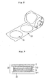
- Fig. 1 is a view of steps for describing a method of thinning a semiconductor wafer according to the present invention and a subsequent dicing process.
- a semiconductor wafer 1 of Fig. 1 (A) has a wiring pattern formed on a front surface 1a thereof, and has a rear surface 1b on the opposite surface thereof.
- the wiring pattern formed on the front surface 1a has a desired pattern formed according to a conventional method.
- a two-sided adhesive sheet 2 is stuck onto front surface 1a of the above-mentioned semiconductor wafer 1, as shown in Fig. 1 (B) .
- the two-sided adhesive sheet 2 has a base material 2a and adhesive layers 2b 1 , 2b 2 , and has a release sheet 2c on adhesive layer 2b 2 .
- Such a two-sided adhesive sheet 2 is stuck onto the semiconductor wafer 1, after peeling a label-shaped one, for example, as shown in Figs. 2 and 3 , which is stamped out into the same shape as semiconductor wafer 1, off from the one supported on a release support sheet 2d, and aligning it with semiconductor wafer 1.
- semiconductor wafer 1 is fixed to a chuck table.
- the two-sided adhesive sheet to be used in the sticking step need not have a label shape stamped out into the same shape as the semiconductor wafer, and may have a sheet shape. In this case, the two-sided adhesive sheet is cut into a shape of the semiconductor wafer after being stuck onto the semiconductor wafer.
- two-sided adhesive sheet 2 those conventionally used as base materials of two-sided adhesive sheets can be used without any particular limitation.
- base material 2a a uniaxially oriented or biaxially oriented film of, for example, polyethylene terephthalate, polyethylene, polystyrene, polypropylene, nylon, urethane, polyvinylidene chloride, polyvinyl chloride, or the likes are exemplified.
- the thickness of base material 2a is usually from about 30 ⁇ m to 200 ⁇ m.
- the adhesive that forms adhesive layers 2b 1 , 2b 2 can be used various adhesives such as acryl-series, rubber-series, silicone-series, polyvinyl ether-series, or the likes, and these may be an energy beam curing type or a foaming type.
- adhesive layer 2b 1 stuck onto semiconductor wafer front surface 1a is made of an adhesive that can reduce its adhesive force to the semiconductor wafer front surface 1a after the thinningprocess, of the thermoreleasing type. because of facility in releasing.
- adhesive layer 2b 2 also is made of an adhesive that can reduce its adhesive force to support wafer 3, of a thermoreleasing type , in the same manner as adhesive layer 2b 1 ; however, as both of adhesive layers 2b 1 , 2b 2 are made of thermoreleasing type adhesives, adhesive layer 2b 2 released in a later step than adhesive layer 2b 1 is made of an adhesive that thermally releases at a higher temperature than adhesive layer 2b 1 .
- Adhesive layers 2b 1 , 2b 2 usually have a thickness of about 20 ⁇ m to 100 ⁇ m.
- REVALPHA (trade name) manufactured by NITTO DENKO Co., Ltd. is exemplified, for example.
- release sheet 2c is peeled off, and support wafer 3 aligned is stuck onto adhesive layer 2b 2 to fabricate a reinforced wafer as shown in Fig. 1(C) .
- sticking a two-sided adhesive sheet onto a support wafer and sticking it onto semiconductor wafer front surface 1a can fabricate a reinforced wafer.
- Support wafer 3 is made of the same material as semiconductor wafer 1. Further, the shape, size, and others of support wafer 3 are not particularly limited as long as a thinning process can be carried out on semiconductor wafer rear surface 1b. Support wafer 3 preferably has the same size as semiconductor wafer 1 as shown in Fig. 1 (C) . Support wafer 3 preferably has a thickness usually of about 400 ⁇ m to 800 ⁇ m.
- the alignment between two-sided adhesive sheet 2 and semiconductor wafer 1 in Fig. 1(B) and the alignment between semiconductor wafer 1 and support wafer 3 in Fig. 1(C) can be carried out using an image recognition apparatus by recognizing the accurate position to compensate for a difference from the current position.
- the position of semiconductor wafer 1 is inverted in an up-and-down direction, and support wafer 3 of the reinforced wafer is chucked to perform a thinning process on semiconductor wafer rear surface 1b.
- the thinning process can be carried out by a conventional method.
- a thinning process machine 4 a grinding machine (back grinding), a CMP pad, and others may be used.
- the thinning process is carried out until semiconductor wafer 1 has a desired thickness.
- the reinforced wafer having finished the thinning process is conveyed to a subsequent dicing step after inverting the position of semiconductor wafer 1 in an up-and-down direction.
- an adhesive tape 5 for dicing is first stuck onto the rear surface 1b of the reinforced wafer, as shown in Fig. 1(E) , to fabricate a wafer mount frame.
- the base material 5a and the adhesive 5b of the adhesive tape for dicing those conventionally known in the art can be used without any particular limitation.
- the support wafer is removed from semiconductor wafer 1, as shown in Fig. 1(F) , and subsequently the semiconductor wafer is divided into chips 1' by a dicing step of Fig. 1(G) .
- the support wafer In removing support wafer 3 from semiconductor wafer 1 in Fig. 1(F) , with a two-sided adhesive sheet 2 made of a thermoreleasing type two-sided adhesive sheet, the support wafer can be easily released by heating the chuck table of the wafer mount frame to an arbitrary temperature to reduce the adhesive force between semiconductor wafer 1 and adhesive layer 2b 1 .
- the adhesive force is reduced by heating to 90°C, thereby facilitating the release of the support wafer.
- the dicing can be carried out without using adhesive tape 5 for dicing (without fabricating the wafer mount frame).
- the support wafer 3 side of the reinforced wafer is chucked, and the dicing is carried out from semiconductor wafer rear surface 1b.
- support wafer 3 is removed by heating to a predetermined temperature to reduce the adhesive force between adhesive layer 2b 1 of the thermoreleasing type two-sided adhesive sheet and semiconductor wafer 1a.
- the method of processing a semiconductor wafer according to the present invention has the following effects.
- By sticking the support wafer onto the semiconductor wafer with the two-sided adhesive sheet sufficient strength and rigidity can be obtained even after a thinning process is carried out. Therefore, it will be easier to handle the semiconductor wafers in the thinning step, and a process using a wafer carrier will be possible as well. Also, the breaking of semiconductor wafers can be restrained to the minimum.
- the support wafer is stuck onto the front surface of the semiconductor wafer with the two-sided adhesive sheet, the protective tape for protecting the front surface of the semiconductor wafer, which tape has been conventionally used in the thinning process, will be no longer needed.
- the support wafer can be an already made product that exists as a semiconductor wafer, and there is no need to fabricate the support wafer separately.
- the support wafer is stuck onto the semiconductor wafer with the two-sided adhesive sheet, the removal thereof is carried out with ease and certainty. Also, by releasing and removing the two-sided adhesive sheet from the support wafer that has been removed from the semiconductor wafer, the support wafer can be reutilized. Usually, one surface of a wafer is finished as a mirror surface. Therefore, by sticking a two-sided adhesive sheet onto the mirror surface side of a support wafer to utilize the support wafer, the releasing is easy with no residual glue, thereby providing advantages in reutilizing the support wafer.
Landscapes
- Engineering & Computer Science (AREA)
- Physics & Mathematics (AREA)
- Condensed Matter Physics & Semiconductors (AREA)
- General Physics & Mathematics (AREA)
- Manufacturing & Machinery (AREA)
- Computer Hardware Design (AREA)
- Microelectronics & Electronic Packaging (AREA)
- Power Engineering (AREA)
- Container, Conveyance, Adherence, Positioning, Of Wafer (AREA)
- Mechanical Treatment Of Semiconductor (AREA)
- Finish Polishing, Edge Sharpening, And Grinding By Specific Grinding Devices (AREA)
- Crystals, And After-Treatments Of Crystals (AREA)
Claims (1)
- Verfahren zum Behandeln eines Halbleiter-Wafers (1),
wobei das Verfahren folgende Schritte aufweist:- Bereitstellen eines Halbleiter-Wafers (1), der eine auf einer vorderen Oberfläche (1a) ausgebildete Struktur aufweist;- Aufbringen eines doppelseitigen Haftflächenkörpers (2) auf der vorderen Oberfläche (1a) des Halbleiter-Wafers (1) mittels einer ersten Klebstoffschicht (2b1);- Aufkleben eines Träger-Wafers (3) auf den doppelseitigen Haftflächenkörper (2) mittels einer zweiten Klebstoffschicht (2b2);- Ausführen eines Verdünnungsvorgangs an einer hinteren Oberfläche (1b) des Halbleiter-Wafers (1) in einem Zustand, in dem der Träger-Wafer (2) an diesem befestigt ist;dadurch gekennzeichnet,
daß der Haftflächenkörper (2) eine zweite Klebstoffschicht (2b2) vom Typ mit thermischer Ablösung zum Festlegen des Träger-Wafers (3) aufweist, die eine thermische Ablösung bei einer höheren Temperatur als die erste Klebstoffschicht (2b1) vom Typ mit thermischer Ablösung ausführt, die an dem Halbleiter-Wafer (1) angebracht ist; und
daß der Träger-Wafer (3) aus dem gleichen Material wie der zu behandelnde Halbleiter-Wafer (1) hergestellt ist.
Applications Claiming Priority (3)
| Application Number | Priority Date | Filing Date | Title |
|---|---|---|---|
| JP2000260924 | 2000-08-30 | ||
| JP2000260924A JP2002075937A (ja) | 2000-08-30 | 2000-08-30 | 半導体ウエハの加工方法 |
| PCT/JP2001/007365 WO2002019393A2 (en) | 2000-08-30 | 2001-08-27 | Method of processing a semiconductor wafer |
Publications (2)
| Publication Number | Publication Date |
|---|---|
| EP1316111A2 EP1316111A2 (de) | 2003-06-04 |
| EP1316111B1 true EP1316111B1 (de) | 2011-02-02 |
Family
ID=18748861
Family Applications (1)
| Application Number | Title | Priority Date | Filing Date |
|---|---|---|---|
| EP01958558A Expired - Lifetime EP1316111B1 (de) | 2000-08-30 | 2001-08-27 | Verfahren zur behandlung eines halbleitenden wafers |
Country Status (9)
| Country | Link |
|---|---|
| US (1) | US6803293B2 (de) |
| EP (1) | EP1316111B1 (de) |
| JP (1) | JP2002075937A (de) |
| KR (1) | KR100811958B1 (de) |
| AT (1) | ATE497634T1 (de) |
| DE (1) | DE60143987D1 (de) |
| PT (1) | PT1316111E (de) |
| TW (1) | TW518721B (de) |
| WO (1) | WO2002019393A2 (de) |
Families Citing this family (23)
| Publication number | Priority date | Publication date | Assignee | Title |
|---|---|---|---|---|
| JP2003209082A (ja) * | 2002-01-15 | 2003-07-25 | Nitto Denko Corp | 保護テープの貼付方法およびその装置並びに保護テープの剥離方法 |
| JP4137471B2 (ja) | 2002-03-04 | 2008-08-20 | 東京エレクトロン株式会社 | ダイシング方法、集積回路チップの検査方法及び基板保持装置 |
| JP2004079889A (ja) * | 2002-08-21 | 2004-03-11 | Disco Abrasive Syst Ltd | 半導体ウェーハの製造方法 |
| JP2005116610A (ja) * | 2003-10-03 | 2005-04-28 | Nitto Denko Corp | 半導体ウエハの加工方法および半導体ウエハ加工用粘着シート |
| DE102004010956B9 (de) * | 2004-03-03 | 2010-08-05 | Infineon Technologies Ag | Halbleiterbauteil mit einem dünnen Halbleiterchip und einem steifen Verdrahtungssubstrat sowie Verfahren zur Herstellung und Weiterverarbeitung von dünnen Halbleiterchips |
| JP4381860B2 (ja) * | 2004-03-24 | 2009-12-09 | 日東電工株式会社 | 補強半導体ウエハに固定された補強板の分離方法およびその装置 |
| US7190058B2 (en) * | 2004-04-01 | 2007-03-13 | Chippac, Inc. | Spacer die structure and method for attaching |
| JP2005302982A (ja) * | 2004-04-12 | 2005-10-27 | Nitto Denko Corp | 半導体チップの製造方法 |
| JP2005340655A (ja) * | 2004-05-28 | 2005-12-08 | Shinko Electric Ind Co Ltd | 半導体装置の製造方法および半導体基板の支持構造体 |
| JP2007095780A (ja) * | 2005-09-27 | 2007-04-12 | Oki Electric Ind Co Ltd | 半導体装置製造用治具と半導体装置製造方法 |
| GB0602410D0 (en) * | 2006-02-07 | 2006-03-15 | Filtronic Compound Semiconduct | A method of bonding a semiconductor wafer to a support substrate |
| DE102006048800B4 (de) | 2006-10-16 | 2018-12-13 | Nissan Chemical Industries, Ltd. | Mehrlagenschichtsystem mit hartem Träger zum Trägern von dünnen Wafern bei der Halbleiterherstellung |
| DE102006009394B4 (de) | 2006-03-01 | 2025-07-31 | Nissan Chemical Industries, Ltd. | Mehrlagenschichtsystem mit einer Schicht als Trennschicht zum Trägern von dünnen Wafern bei der Halbleiterherstellung, Verwendung des Schichtsystems beim und Verfahren zum Abdünnen eines Wafers |
| DE102006048799B4 (de) | 2006-10-16 | 2018-09-20 | Nissan Chemical Industries, Ltd. | Verfahren und Einrichtung zum Ablösen eines dünnen Wafers oder bereits vereinzelter Bauelemente eines dünnen Wafers von einem Träger |
| DE102006009353B4 (de) | 2006-03-01 | 2025-03-27 | Nissan Chemical Industries, Ltd. | Mehrlagenschichtsystem zum Trägern von dünnen Wafern bei der Halbleiterherstellung mit der Eigenschaft zum Haltern mittels elektrostatischer Aufladung |
| JP5027460B2 (ja) * | 2006-07-28 | 2012-09-19 | 東京応化工業株式会社 | ウエハの接着方法、薄板化方法、及び剥離方法 |
| JP5190222B2 (ja) * | 2007-06-01 | 2013-04-24 | 日東電工株式会社 | 両面発泡粘着シートおよび液晶表示装置 |
| JP2010056562A (ja) * | 2009-11-26 | 2010-03-11 | Nitto Denko Corp | 半導体チップの製造方法 |
| JP5348075B2 (ja) * | 2010-06-02 | 2013-11-20 | ソニー株式会社 | 半導体発光素子の製造方法、半導体素子の製造方法および素子の製造方法 |
| GB2481187B (en) | 2010-06-04 | 2014-10-29 | Plastic Logic Ltd | Processing substrates |
| JP5591859B2 (ja) * | 2012-03-23 | 2014-09-17 | 株式会社東芝 | 基板の分離方法及び分離装置 |
| JP2015217461A (ja) * | 2014-05-16 | 2015-12-07 | 株式会社ディスコ | ウェーハの加工方法 |
| CN106206382A (zh) * | 2016-08-30 | 2016-12-07 | 浙江中纳晶微电子科技有限公司 | 薄片状工件临时键合的加工方法 |
Family Cites Families (12)
| Publication number | Priority date | Publication date | Assignee | Title |
|---|---|---|---|---|
| JPS5956471A (ja) | 1982-09-24 | 1984-03-31 | Nitto Electric Ind Co Ltd | 両面接着テ−プの製造方法 |
| JPH05291397A (ja) | 1992-04-07 | 1993-11-05 | Toshiba Corp | コレットおよび半導体装置の製造方法 |
| US5476566A (en) * | 1992-09-02 | 1995-12-19 | Motorola, Inc. | Method for thinning a semiconductor wafer |
| JPH0774131A (ja) * | 1993-09-02 | 1995-03-17 | Matsushita Electric Ind Co Ltd | ダイシング装置及び半導体チップの加工方法 |
| US6342434B1 (en) * | 1995-12-04 | 2002-01-29 | Hitachi, Ltd. | Methods of processing semiconductor wafer, and producing IC card, and carrier |
| JPH10284449A (ja) * | 1997-04-11 | 1998-10-23 | Disco Abrasive Syst Ltd | ウェーハの裏面研磨・ダイシング方法及びシステム |
| ATE230277T1 (de) | 1997-06-13 | 2003-01-15 | Genentech Inc | Stabilisierte antikörperformulierung |
| US6162703A (en) * | 1998-02-23 | 2000-12-19 | Micron Technology, Inc. | Packaging die preparation |
| JP2000038556A (ja) * | 1998-07-22 | 2000-02-08 | Nitto Denko Corp | 半導体ウエハ保持保護用ホットメルトシート及びその貼り付け方法 |
| JP3784202B2 (ja) * | 1998-08-26 | 2006-06-07 | リンテック株式会社 | 両面粘着シートおよびその使用方法 |
| DE19850873A1 (de) | 1998-11-05 | 2000-05-11 | Philips Corp Intellectual Pty | Verfahren zum Bearbeiten eines Erzeugnisses der Halbleitertechnik |
| DE19962763C2 (de) | 1999-07-01 | 2001-07-26 | Fraunhofer Ges Forschung | Verfahren zum Vereinzeln eines Wafers |
-
2000
- 2000-08-30 JP JP2000260924A patent/JP2002075937A/ja active Pending
-
2001
- 2001-07-31 TW TW090118683A patent/TW518721B/zh not_active IP Right Cessation
- 2001-08-27 US US10/362,489 patent/US6803293B2/en not_active Expired - Fee Related
- 2001-08-27 AT AT01958558T patent/ATE497634T1/de active
- 2001-08-27 KR KR1020037002881A patent/KR100811958B1/ko not_active Expired - Fee Related
- 2001-08-27 EP EP01958558A patent/EP1316111B1/de not_active Expired - Lifetime
- 2001-08-27 PT PT01958558T patent/PT1316111E/pt unknown
- 2001-08-27 DE DE60143987T patent/DE60143987D1/de not_active Expired - Lifetime
- 2001-08-27 WO PCT/JP2001/007365 patent/WO2002019393A2/en not_active Ceased
Also Published As
| Publication number | Publication date |
|---|---|
| PT1316111E (pt) | 2011-03-23 |
| WO2002019393A3 (en) | 2002-06-06 |
| ATE497634T1 (de) | 2011-02-15 |
| US20040038469A1 (en) | 2004-02-26 |
| JP2002075937A (ja) | 2002-03-15 |
| EP1316111A2 (de) | 2003-06-04 |
| KR20030029152A (ko) | 2003-04-11 |
| KR100811958B1 (ko) | 2008-03-10 |
| DE60143987D1 (de) | 2011-03-17 |
| US6803293B2 (en) | 2004-10-12 |
| TW518721B (en) | 2003-01-21 |
| WO2002019393A2 (en) | 2002-03-07 |
Similar Documents
| Publication | Publication Date | Title |
|---|---|---|
| EP1316111B1 (de) | Verfahren zur behandlung eines halbleitenden wafers | |
| JP3784202B2 (ja) | 両面粘着シートおよびその使用方法 | |
| JP4762671B2 (ja) | ダイシングテープ、および半導体ウェハダイシング方法 | |
| US5476566A (en) | Method for thinning a semiconductor wafer | |
| US5897743A (en) | Jig for peeling a bonded wafer | |
| KR102070031B1 (ko) | 반도체 웨이퍼의 처리 방법, 반도체 칩 및 표면 보호 테이프 | |
| US6312800B1 (en) | Pressure sensitive adhesive sheet for producing a chip | |
| US20070218649A1 (en) | Semiconductor wafer thinning | |
| US6777310B2 (en) | Method of fabricating semiconductor devices on a semiconductor wafer using a carrier plate during grinding and dicing steps | |
| JP2001217212A (ja) | 半導体チップの製造方法 | |
| JP2000129227A (ja) | 半導体ウエハ保護用粘着シートおよびその使用方法 | |
| JP2000331962A (ja) | 半導体ウエハの加工方法および半導体ウエハ支持部材 | |
| TWI649798B (zh) | 遮罩一體型表面保護帶 | |
| US7504316B2 (en) | Method and device for separating a reinforcing-plate fixed to a reinforced semiconductor wafer | |
| JPH11307488A (ja) | 半導体装置、その製造方法、加工ガイドおよびその加工装置 | |
| JP4757442B2 (ja) | チップ体製造用粘着シート | |
| JP4234630B2 (ja) | 貫通構造を有する薄膜化回路基板の製造方法と保護用粘着テープ | |
| EP1316992B1 (de) | Verfahren zur Bearbeitung einer Halbleiterscheibe, in dem ein laminiertes Substrat als Stütze für diese Scheibe verwendet wird | |
| JP2005302982A (ja) | 半導体チップの製造方法 | |
| JP2005116948A (ja) | 半導体ウエハの加工方法およびそれに用いる両面粘着シート | |
| JP4768963B2 (ja) | ウェハの転写方法 | |
| JP2002270560A (ja) | ウエハの加工方法 | |
| JPH10233373A (ja) | チップ体の製造方法および該製造方法に用いられる粘着シート | |
| US20030073264A1 (en) | Method of manufacturing semiconductor device from semiconductor wafer having thick peripheral portion | |
| JP4180557B2 (ja) | 両面粘着シート |
Legal Events
| Date | Code | Title | Description |
|---|---|---|---|
| PUAI | Public reference made under article 153(3) epc to a published international application that has entered the european phase |
Free format text: ORIGINAL CODE: 0009012 |
|
| 17P | Request for examination filed |
Effective date: 20030331 |
|
| AK | Designated contracting states |
Designated state(s): AT BE CH CY DE DK ES FI FR GB GR IE IT LI LU MC NL PT SE TR |
|
| 17Q | First examination report despatched |
Effective date: 20090109 |
|
| GRAP | Despatch of communication of intention to grant a patent |
Free format text: ORIGINAL CODE: EPIDOSNIGR1 |
|
| GRAS | Grant fee paid |
Free format text: ORIGINAL CODE: EPIDOSNIGR3 |
|
| GRAA | (expected) grant |
Free format text: ORIGINAL CODE: 0009210 |
|
| AK | Designated contracting states |
Kind code of ref document: B1 Designated state(s): AT BE CH CY DE DK ES FI FR GB GR IE IT LI LU MC NL PT SE TR |
|
| REG | Reference to a national code |
Ref country code: GB Ref legal event code: FG4D |
|
| REG | Reference to a national code |
Ref country code: CH Ref legal event code: EP |
|
| REG | Reference to a national code |
Ref country code: CH Ref legal event code: NV Representative=s name: TROESCH SCHEIDEGGER WERNER AG |
|
| REG | Reference to a national code |
Ref country code: IE Ref legal event code: FG4D |
|
| REF | Corresponds to: |
Ref document number: 60143987 Country of ref document: DE Date of ref document: 20110317 Kind code of ref document: P |
|
| REG | Reference to a national code |
Ref country code: DE Ref legal event code: R096 Ref document number: 60143987 Country of ref document: DE Effective date: 20110317 |
|
| REG | Reference to a national code |
Ref country code: PT Ref legal event code: SC4A Free format text: AVAILABILITY OF NATIONAL TRANSLATION Effective date: 20110315 |
|
| REG | Reference to a national code |
Ref country code: NL Ref legal event code: VDEP Effective date: 20110202 |
|
| PG25 | Lapsed in a contracting state [announced via postgrant information from national office to epo] |
Ref country code: ES Free format text: LAPSE BECAUSE OF FAILURE TO SUBMIT A TRANSLATION OF THE DESCRIPTION OR TO PAY THE FEE WITHIN THE PRESCRIBED TIME-LIMIT Effective date: 20110513 Ref country code: GR Free format text: LAPSE BECAUSE OF FAILURE TO SUBMIT A TRANSLATION OF THE DESCRIPTION OR TO PAY THE FEE WITHIN THE PRESCRIBED TIME-LIMIT Effective date: 20110503 Ref country code: SE Free format text: LAPSE BECAUSE OF FAILURE TO SUBMIT A TRANSLATION OF THE DESCRIPTION OR TO PAY THE FEE WITHIN THE PRESCRIBED TIME-LIMIT Effective date: 20110202 |
|
| PG25 | Lapsed in a contracting state [announced via postgrant information from national office to epo] |
Ref country code: NL Free format text: LAPSE BECAUSE OF FAILURE TO SUBMIT A TRANSLATION OF THE DESCRIPTION OR TO PAY THE FEE WITHIN THE PRESCRIBED TIME-LIMIT Effective date: 20110202 Ref country code: FI Free format text: LAPSE BECAUSE OF FAILURE TO SUBMIT A TRANSLATION OF THE DESCRIPTION OR TO PAY THE FEE WITHIN THE PRESCRIBED TIME-LIMIT Effective date: 20110202 Ref country code: CY Free format text: LAPSE BECAUSE OF FAILURE TO SUBMIT A TRANSLATION OF THE DESCRIPTION OR TO PAY THE FEE WITHIN THE PRESCRIBED TIME-LIMIT Effective date: 20110202 Ref country code: BE Free format text: LAPSE BECAUSE OF FAILURE TO SUBMIT A TRANSLATION OF THE DESCRIPTION OR TO PAY THE FEE WITHIN THE PRESCRIBED TIME-LIMIT Effective date: 20110202 |
|
| PG25 | Lapsed in a contracting state [announced via postgrant information from national office to epo] |
Ref country code: DK Free format text: LAPSE BECAUSE OF FAILURE TO SUBMIT A TRANSLATION OF THE DESCRIPTION OR TO PAY THE FEE WITHIN THE PRESCRIBED TIME-LIMIT Effective date: 20110202 |
|
| PLBE | No opposition filed within time limit |
Free format text: ORIGINAL CODE: 0009261 |
|
| STAA | Information on the status of an ep patent application or granted ep patent |
Free format text: STATUS: NO OPPOSITION FILED WITHIN TIME LIMIT |
|
| 26N | No opposition filed |
Effective date: 20111103 |
|
| REG | Reference to a national code |
Ref country code: DE Ref legal event code: R097 Ref document number: 60143987 Country of ref document: DE Effective date: 20111103 |
|
| PG25 | Lapsed in a contracting state [announced via postgrant information from national office to epo] |
Ref country code: MC Free format text: LAPSE BECAUSE OF NON-PAYMENT OF DUE FEES Effective date: 20110831 |
|
| REG | Reference to a national code |
Ref country code: CH Ref legal event code: PL |
|
| GBPC | Gb: european patent ceased through non-payment of renewal fee |
Effective date: 20110827 |
|
| PG25 | Lapsed in a contracting state [announced via postgrant information from national office to epo] |
Ref country code: LI Free format text: LAPSE BECAUSE OF NON-PAYMENT OF DUE FEES Effective date: 20110831 Ref country code: CH Free format text: LAPSE BECAUSE OF NON-PAYMENT OF DUE FEES Effective date: 20110831 |
|
| REG | Reference to a national code |
Ref country code: FR Ref legal event code: ST Effective date: 20120430 |
|
| REG | Reference to a national code |
Ref country code: IE Ref legal event code: MM4A |
|
| PG25 | Lapsed in a contracting state [announced via postgrant information from national office to epo] |
Ref country code: IT Free format text: LAPSE BECAUSE OF NON-PAYMENT OF DUE FEES Effective date: 20110827 |
|
| REG | Reference to a national code |
Ref country code: PT Ref legal event code: MM4A Free format text: LAPSE DUE TO NON-PAYMENT OF FEES Effective date: 20120528 |
|
| PG25 | Lapsed in a contracting state [announced via postgrant information from national office to epo] |
Ref country code: IE Free format text: LAPSE BECAUSE OF NON-PAYMENT OF DUE FEES Effective date: 20110827 |
|
| PG25 | Lapsed in a contracting state [announced via postgrant information from national office to epo] |
Ref country code: GB Free format text: LAPSE BECAUSE OF NON-PAYMENT OF DUE FEES Effective date: 20110827 Ref country code: FR Free format text: LAPSE BECAUSE OF NON-PAYMENT OF DUE FEES Effective date: 20110831 Ref country code: PT Free format text: LAPSE BECAUSE OF NON-PAYMENT OF DUE FEES Effective date: 20120528 |
|
| PG25 | Lapsed in a contracting state [announced via postgrant information from national office to epo] |
Ref country code: LU Free format text: LAPSE BECAUSE OF NON-PAYMENT OF DUE FEES Effective date: 20110827 |
|
| PG25 | Lapsed in a contracting state [announced via postgrant information from national office to epo] |
Ref country code: TR Free format text: LAPSE BECAUSE OF FAILURE TO SUBMIT A TRANSLATION OF THE DESCRIPTION OR TO PAY THE FEE WITHIN THE PRESCRIBED TIME-LIMIT Effective date: 20110202 |
|
| PGFP | Annual fee paid to national office [announced via postgrant information from national office to epo] |
Ref country code: AT Payment date: 20140827 Year of fee payment: 14 |
|
| PGFP | Annual fee paid to national office [announced via postgrant information from national office to epo] |
Ref country code: DE Payment date: 20141031 Year of fee payment: 14 |
|
| REG | Reference to a national code |
Ref country code: DE Ref legal event code: R119 Ref document number: 60143987 Country of ref document: DE |
|
| REG | Reference to a national code |
Ref country code: AT Ref legal event code: MM01 Ref document number: 497634 Country of ref document: AT Kind code of ref document: T Effective date: 20150827 |
|
| PG25 | Lapsed in a contracting state [announced via postgrant information from national office to epo] |
Ref country code: AT Free format text: LAPSE BECAUSE OF NON-PAYMENT OF DUE FEES Effective date: 20150827 |
|
| PG25 | Lapsed in a contracting state [announced via postgrant information from national office to epo] |
Ref country code: DE Free format text: LAPSE BECAUSE OF NON-PAYMENT OF DUE FEES Effective date: 20160301 |