EP1308741B1 - Magnetoresistiver Sensor und sein Herstellungsverfahren - Google Patents
Magnetoresistiver Sensor und sein Herstellungsverfahren Download PDFInfo
- Publication number
- EP1308741B1 EP1308741B1 EP02251657A EP02251657A EP1308741B1 EP 1308741 B1 EP1308741 B1 EP 1308741B1 EP 02251657 A EP02251657 A EP 02251657A EP 02251657 A EP02251657 A EP 02251657A EP 1308741 B1 EP1308741 B1 EP 1308741B1
- Authority
- EP
- European Patent Office
- Prior art keywords
- film
- electrode layer
- lower electrode
- magnetoresistive
- conducting path
- Prior art date
- Legal status (The legal status is an assumption and is not a legal conclusion. Google has not performed a legal analysis and makes no representation as to the accuracy of the status listed.)
- Expired - Lifetime
Links
Images




Classifications
-
- G—PHYSICS
- G01—MEASURING; TESTING
- G01R—MEASURING ELECTRIC VARIABLES; MEASURING MAGNETIC VARIABLES
- G01R33/00—Arrangements or instruments for measuring magnetic variables
- G01R33/02—Measuring direction or magnitude of magnetic fields or magnetic flux
- G01R33/06—Measuring direction or magnitude of magnetic fields or magnetic flux using galvano-magnetic devices
- G01R33/09—Magnetoresistive devices
-
- G—PHYSICS
- G11—INFORMATION STORAGE
- G11B—INFORMATION STORAGE BASED ON RELATIVE MOVEMENT BETWEEN RECORD CARRIER AND TRANSDUCER
- G11B5/00—Recording by magnetisation or demagnetisation of a record carrier; Reproducing by magnetic means; Record carriers therefor
- G11B5/127—Structure or manufacture of heads, e.g. inductive
- G11B5/33—Structure or manufacture of flux-sensitive heads, i.e. for reproduction only; Combination of such heads with means for recording or erasing only
- G11B5/39—Structure or manufacture of flux-sensitive heads, i.e. for reproduction only; Combination of such heads with means for recording or erasing only using magneto-resistive devices or effects
-
- B—PERFORMING OPERATIONS; TRANSPORTING
- B82—NANOTECHNOLOGY
- B82Y—SPECIFIC USES OR APPLICATIONS OF NANOSTRUCTURES; MEASUREMENT OR ANALYSIS OF NANOSTRUCTURES; MANUFACTURE OR TREATMENT OF NANOSTRUCTURES
- B82Y10/00—Nanotechnology for information processing, storage or transmission, e.g. quantum computing or single electron logic
-
- B—PERFORMING OPERATIONS; TRANSPORTING
- B82—NANOTECHNOLOGY
- B82Y—SPECIFIC USES OR APPLICATIONS OF NANOSTRUCTURES; MEASUREMENT OR ANALYSIS OF NANOSTRUCTURES; MANUFACTURE OR TREATMENT OF NANOSTRUCTURES
- B82Y25/00—Nanomagnetism, e.g. magnetoimpedance, anisotropic magnetoresistance, giant magnetoresistance or tunneling magnetoresistance
-
- G—PHYSICS
- G11—INFORMATION STORAGE
- G11B—INFORMATION STORAGE BASED ON RELATIVE MOVEMENT BETWEEN RECORD CARRIER AND TRANSDUCER
- G11B5/00—Recording by magnetisation or demagnetisation of a record carrier; Reproducing by magnetic means; Record carriers therefor
- G11B5/127—Structure or manufacture of heads, e.g. inductive
- G11B5/33—Structure or manufacture of flux-sensitive heads, i.e. for reproduction only; Combination of such heads with means for recording or erasing only
- G11B5/39—Structure or manufacture of flux-sensitive heads, i.e. for reproduction only; Combination of such heads with means for recording or erasing only using magneto-resistive devices or effects
- G11B5/3903—Structure or manufacture of flux-sensitive heads, i.e. for reproduction only; Combination of such heads with means for recording or erasing only using magneto-resistive devices or effects using magnetic thin film layers or their effects, the films being part of integrated structures
-
- G—PHYSICS
- G11—INFORMATION STORAGE
- G11B—INFORMATION STORAGE BASED ON RELATIVE MOVEMENT BETWEEN RECORD CARRIER AND TRANSDUCER
- G11B5/00—Recording by magnetisation or demagnetisation of a record carrier; Reproducing by magnetic means; Record carriers therefor
- G11B5/127—Structure or manufacture of heads, e.g. inductive
- G11B5/33—Structure or manufacture of flux-sensitive heads, i.e. for reproduction only; Combination of such heads with means for recording or erasing only
- G11B5/39—Structure or manufacture of flux-sensitive heads, i.e. for reproduction only; Combination of such heads with means for recording or erasing only using magneto-resistive devices or effects
- G11B5/3903—Structure or manufacture of flux-sensitive heads, i.e. for reproduction only; Combination of such heads with means for recording or erasing only using magneto-resistive devices or effects using magnetic thin film layers or their effects, the films being part of integrated structures
- G11B5/3906—Details related to the use of magnetic thin film layers or to their effects
- G11B5/3909—Arrangements using a magnetic tunnel junction
-
- H—ELECTRICITY
- H10—SEMICONDUCTOR DEVICES; ELECTRIC SOLID-STATE DEVICES NOT OTHERWISE PROVIDED FOR
- H10N—ELECTRIC SOLID-STATE DEVICES NOT OTHERWISE PROVIDED FOR
- H10N50/00—Galvanomagnetic devices
- H10N50/10—Magnetoresistive devices
-
- G—PHYSICS
- G11—INFORMATION STORAGE
- G11B—INFORMATION STORAGE BASED ON RELATIVE MOVEMENT BETWEEN RECORD CARRIER AND TRANSDUCER
- G11B5/00—Recording by magnetisation or demagnetisation of a record carrier; Reproducing by magnetic means; Record carriers therefor
- G11B5/127—Structure or manufacture of heads, e.g. inductive
- G11B5/33—Structure or manufacture of flux-sensitive heads, i.e. for reproduction only; Combination of such heads with means for recording or erasing only
- G11B5/39—Structure or manufacture of flux-sensitive heads, i.e. for reproduction only; Combination of such heads with means for recording or erasing only using magneto-resistive devices or effects
- G11B2005/3996—Structure or manufacture of flux-sensitive heads, i.e. for reproduction only; Combination of such heads with means for recording or erasing only using magneto-resistive devices or effects large or giant magnetoresistive effects [GMR], e.g. as generated in spin-valve [SV] devices
-
- Y—GENERAL TAGGING OF NEW TECHNOLOGICAL DEVELOPMENTS; GENERAL TAGGING OF CROSS-SECTIONAL TECHNOLOGIES SPANNING OVER SEVERAL SECTIONS OF THE IPC; TECHNICAL SUBJECTS COVERED BY FORMER USPC CROSS-REFERENCE ART COLLECTIONS [XRACs] AND DIGESTS
- Y10—TECHNICAL SUBJECTS COVERED BY FORMER USPC
- Y10T—TECHNICAL SUBJECTS COVERED BY FORMER US CLASSIFICATION
- Y10T428/00—Stock material or miscellaneous articles
- Y10T428/11—Magnetic recording head
- Y10T428/1107—Magnetoresistive
-
- Y—GENERAL TAGGING OF NEW TECHNOLOGICAL DEVELOPMENTS; GENERAL TAGGING OF CROSS-SECTIONAL TECHNOLOGIES SPANNING OVER SEVERAL SECTIONS OF THE IPC; TECHNICAL SUBJECTS COVERED BY FORMER USPC CROSS-REFERENCE ART COLLECTIONS [XRACs] AND DIGESTS
- Y10—TECHNICAL SUBJECTS COVERED BY FORMER USPC
- Y10T—TECHNICAL SUBJECTS COVERED BY FORMER US CLASSIFICATION
- Y10T428/00—Stock material or miscellaneous articles
- Y10T428/12—All metal or with adjacent metals
- Y10T428/12465—All metal or with adjacent metals having magnetic properties, or preformed fiber orientation coordinate with shape
-
- Y—GENERAL TAGGING OF NEW TECHNOLOGICAL DEVELOPMENTS; GENERAL TAGGING OF CROSS-SECTIONAL TECHNOLOGIES SPANNING OVER SEVERAL SECTIONS OF THE IPC; TECHNICAL SUBJECTS COVERED BY FORMER USPC CROSS-REFERENCE ART COLLECTIONS [XRACs] AND DIGESTS
- Y10—TECHNICAL SUBJECTS COVERED BY FORMER USPC
- Y10T—TECHNICAL SUBJECTS COVERED BY FORMER US CLASSIFICATION
- Y10T428/00—Stock material or miscellaneous articles
- Y10T428/12—All metal or with adjacent metals
- Y10T428/12493—Composite; i.e., plural, adjacent, spatially distinct metal components [e.g., layers, joint, etc.]
- Y10T428/12535—Composite; i.e., plural, adjacent, spatially distinct metal components [e.g., layers, joint, etc.] with additional, spatially distinct nonmetal component
-
- Y—GENERAL TAGGING OF NEW TECHNOLOGICAL DEVELOPMENTS; GENERAL TAGGING OF CROSS-SECTIONAL TECHNOLOGIES SPANNING OVER SEVERAL SECTIONS OF THE IPC; TECHNICAL SUBJECTS COVERED BY FORMER USPC CROSS-REFERENCE ART COLLECTIONS [XRACs] AND DIGESTS
- Y10—TECHNICAL SUBJECTS COVERED BY FORMER USPC
- Y10T—TECHNICAL SUBJECTS COVERED BY FORMER US CLASSIFICATION
- Y10T428/00—Stock material or miscellaneous articles
- Y10T428/12—All metal or with adjacent metals
- Y10T428/12493—Composite; i.e., plural, adjacent, spatially distinct metal components [e.g., layers, joint, etc.]
- Y10T428/12535—Composite; i.e., plural, adjacent, spatially distinct metal components [e.g., layers, joint, etc.] with additional, spatially distinct nonmetal component
- Y10T428/12611—Oxide-containing component
-
- Y—GENERAL TAGGING OF NEW TECHNOLOGICAL DEVELOPMENTS; GENERAL TAGGING OF CROSS-SECTIONAL TECHNOLOGIES SPANNING OVER SEVERAL SECTIONS OF THE IPC; TECHNICAL SUBJECTS COVERED BY FORMER USPC CROSS-REFERENCE ART COLLECTIONS [XRACs] AND DIGESTS
- Y10—TECHNICAL SUBJECTS COVERED BY FORMER USPC
- Y10T—TECHNICAL SUBJECTS COVERED BY FORMER US CLASSIFICATION
- Y10T428/00—Stock material or miscellaneous articles
- Y10T428/13—Hollow or container type article [e.g., tube, vase, etc.]
-
- Y—GENERAL TAGGING OF NEW TECHNOLOGICAL DEVELOPMENTS; GENERAL TAGGING OF CROSS-SECTIONAL TECHNOLOGIES SPANNING OVER SEVERAL SECTIONS OF THE IPC; TECHNICAL SUBJECTS COVERED BY FORMER USPC CROSS-REFERENCE ART COLLECTIONS [XRACs] AND DIGESTS
- Y10—TECHNICAL SUBJECTS COVERED BY FORMER USPC
- Y10T—TECHNICAL SUBJECTS COVERED BY FORMER US CLASSIFICATION
- Y10T428/00—Stock material or miscellaneous articles
- Y10T428/249921—Web or sheet containing structurally defined element or component
- Y10T428/249953—Composite having voids in a component [e.g., porous, cellular, etc.]
- Y10T428/249971—Preformed hollow element-containing
- Y10T428/249974—Metal- or silicon-containing element
-
- Y—GENERAL TAGGING OF NEW TECHNOLOGICAL DEVELOPMENTS; GENERAL TAGGING OF CROSS-SECTIONAL TECHNOLOGIES SPANNING OVER SEVERAL SECTIONS OF THE IPC; TECHNICAL SUBJECTS COVERED BY FORMER USPC CROSS-REFERENCE ART COLLECTIONS [XRACs] AND DIGESTS
- Y10—TECHNICAL SUBJECTS COVERED BY FORMER USPC
- Y10T—TECHNICAL SUBJECTS COVERED BY FORMER US CLASSIFICATION
- Y10T428/00—Stock material or miscellaneous articles
- Y10T428/25—Web or sheet containing structurally defined element or component and including a second component containing structurally defined particles
-
- Y—GENERAL TAGGING OF NEW TECHNOLOGICAL DEVELOPMENTS; GENERAL TAGGING OF CROSS-SECTIONAL TECHNOLOGIES SPANNING OVER SEVERAL SECTIONS OF THE IPC; TECHNICAL SUBJECTS COVERED BY FORMER USPC CROSS-REFERENCE ART COLLECTIONS [XRACs] AND DIGESTS
- Y10—TECHNICAL SUBJECTS COVERED BY FORMER USPC
- Y10T—TECHNICAL SUBJECTS COVERED BY FORMER US CLASSIFICATION
- Y10T428/00—Stock material or miscellaneous articles
- Y10T428/29—Coated or structually defined flake, particle, cell, strand, strand portion, rod, filament, macroscopic fiber or mass thereof
- Y10T428/2913—Rod, strand, filament or fiber
- Y10T428/2918—Rod, strand, filament or fiber including free carbon or carbide or therewith [not as steel]
-
- Y—GENERAL TAGGING OF NEW TECHNOLOGICAL DEVELOPMENTS; GENERAL TAGGING OF CROSS-SECTIONAL TECHNOLOGIES SPANNING OVER SEVERAL SECTIONS OF THE IPC; TECHNICAL SUBJECTS COVERED BY FORMER USPC CROSS-REFERENCE ART COLLECTIONS [XRACs] AND DIGESTS
- Y10—TECHNICAL SUBJECTS COVERED BY FORMER USPC
- Y10T—TECHNICAL SUBJECTS COVERED BY FORMER US CLASSIFICATION
- Y10T428/00—Stock material or miscellaneous articles
- Y10T428/29—Coated or structually defined flake, particle, cell, strand, strand portion, rod, filament, macroscopic fiber or mass thereof
- Y10T428/2913—Rod, strand, filament or fiber
- Y10T428/2933—Coated or with bond, impregnation or core
- Y10T428/2964—Artificial fiber or filament
-
- Y—GENERAL TAGGING OF NEW TECHNOLOGICAL DEVELOPMENTS; GENERAL TAGGING OF CROSS-SECTIONAL TECHNOLOGIES SPANNING OVER SEVERAL SECTIONS OF THE IPC; TECHNICAL SUBJECTS COVERED BY FORMER USPC CROSS-REFERENCE ART COLLECTIONS [XRACs] AND DIGESTS
- Y10—TECHNICAL SUBJECTS COVERED BY FORMER USPC
- Y10T—TECHNICAL SUBJECTS COVERED BY FORMER US CLASSIFICATION
- Y10T428/00—Stock material or miscellaneous articles
- Y10T428/29—Coated or structually defined flake, particle, cell, strand, strand portion, rod, filament, macroscopic fiber or mass thereof
- Y10T428/2913—Rod, strand, filament or fiber
- Y10T428/2973—Particular cross section
- Y10T428/2975—Tubular or cellular
Definitions
- the present invention relates to a magnetoresistive sensor for use in a magnetic recording device such as a magnetic disk drive and a magnetic tape drive.
- a head slider With a reduction in size and an increase in recording density of a magnetic disk drive in recent years, the flying height of a head slider has become smaller. It is desirable to realize contact recording/reproduction such that the head slider flies a very small height above a recording medium or comes into contact with the recording medium. Further, a previously-proposed magnetic induction head has the disadvantage that its reproduction output decreases with a decrease in peripheral speed (relative speed between the head and the medium) of a magnetic disk used as the recording medium, which decrease in speed is caused by a reduction in diameter of the magnetic disk.
- MR head magnetoresistive head
- GMR giant magnetoresistive
- the recording density of a magnetic disk drive currently on the market is about 10 Gbit/in 2 , and it is rising at an annual rate of about 200%. It is therefore desirable to develop a magnetoresistive sensor and a magnetoresistive head which can support a minute magnetic field range and can sense a change in small external magnetic fields.
- a spin valve magnetoresistive sensor utilizing a spin valve GMR effect is widely used in a magnetic head.
- a magnetization direction in a free ferromagnetic layer (free layer) is changed by a signal magnetic field from a recording medium, so that a relative angle of this magnetization direction to a magnetization direction in a pinned ferromagnetic layer (pinned layer) is changed, causing a change in resistance of the magnetoresistive sensor.
- the magnetization direction in the pinned layer is fixed to a direction parallel to the height of a magnetoresistive element, and the magnetization direction in the free layer in the condition where no external magnetic field is applied is typically designed to be in a direction parallel to the width of the magnetoresistive element, which direction is perpendicular to the pinned layer.
- the resistance of the magnetoresistive sensor can be linearly increased or decreased according to whether the direction of the signal magnetic field from the magnetic recording medium is parallel or antiparallel to the magnetization direction of the pinned layer.
- a linear resistance change facilitates signal processing in the magnetic disk drive.
- a sense current is passed in a direction parallel to the film surface of the magnetoresistive element in order to determine the resistance change due to an external magnetic field.
- CIP Current In the Plane
- the distance between the upper and lower magnetic shields is equal to the sum of the thickness of the GMR film and a value twice the thickness of each insulating film.
- a minimum thickness of about 20 nm can be obtained for the insulating film.
- the distance between the upper and lower magnetic shields becomes equal to the sum of the thickness of the GMR film and is about 40 nm.
- a magnetic head having a CIP structure utilizing a spin valve GMR effect can support a recording density of 20 to 40 Gbit/in 2 at the maximum. Even by applying the latest technique, specular scattering, the maximum recording density is considered to be 60 Gbit/in 2 .
- the increase in recording density of a magnetic disk drive is rapid, and it is expected that a recording density of 80 Gbit/in 2 will be desired by 2002.
- the recording density becomes 80 Gbit/in 2 or higher it is very difficult to support such a high recording density even by using a CIP spin valve GMR magnetic head to which the latest specular scattering is applied, from the viewpoints of output and the distance between the magnetic shields.
- TMR tunnel MR
- CPP Current Perpendicular to the Plane
- the structure of the TMR is such that a thin insulating layer is sandwiched between two ferromagnetic layers.
- the magnitude of tunnel current passing across the insulating layer is changed according to the magnetization directions in the two ferromagnetic layers.
- the TMR shows a very large resistance change and has a good sensitivity, thus it is expected to be a promising post spin valve GMR.
- the output increases with a decrease in sectional area of a portion of the GMR film where a sense current is passed.
- This feature of the CPP structure makes it more advantageous to use than the CIP structure.
- the TMR is also considered to be a kind of CPP structure, because a current is passed across the insulating layer from one of the ferromagnetic layers to the other ferromagnetic layer. Therefore, the TMR also has the above advantage.
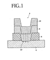
- FIG. 1 of the accompanying drawings shows a schematic sectional view of a previously-proposed magnetoresistive sensor 2 having a CPP structure.
- the magnetoresistive sensor 2 is composed of a lower electrode layer 4, an insulator matrix 6, a magnetoresistive film 8, and an upper electrode layer 10.
- a contact hole 12 is formed at a substantially central portion of the insulator matrix 6.
- the magnetoresistive film 8 is in contact with the lower electrode layer 4 at the contact hole 12.
- a sense current is passed from the upper electrode layer 10, through the contact hole 12 of the magnetoresistive film 8, toward the lower electrode layer 4.
- Dry etching suitable for microfabrication is used for the formation of the contact hole 12.
- the relation between the output ⁇ R from the magnetoresistive sensor 2 and the diameter D of the contact hole 12 is expressed as follows: ⁇ R ⁇ 1/D 2
- the electrical connection of two conductors between which an insulator is interposed is established by a circular hole (contact hole) formed in the insulator.
- the contact hole is formed by dry etching, which is suitable for the microfabrication of devices.
- Dry etching is a process including decomposing a supplied gas by a plasma to generate active species such as ions and radicals, and exposing a substrate to the active species to cause a reaction between the active species and a material to be etched, thereby performing patterning and resist removal.
- active species such as ions and radicals
- the minimum diameter of a contact hole formed by a current dry etching technique is 200 nm in the case of using an i-line stepper or 100 nm even in the case of using an FIB (Focused Ion Beam). In the latter case, there is an intrinsic problem that metal atoms adhere to a sidewall.
- a magnetoresistive sensor with a contact hole of microscopic size of the order of nanometers, with a view to increasing output and, therefore, improving sensitivity.
- JP 2001-143227 discloses a magnetoresistive sensor comprising upper and lower electrode layers, a conducting path layer provided between the upper and lower electrode layers, and a magnetoresistive film provided between the conducting path layer and the lower electrode layer.
- the conducting path layer is formed from an insulator matrix in which are dispersed granular metal particles.
- a magnetoresistive sensor comprising: upper and lower electrode layers; a conducting path layer provided between said upper and lower electrode layers; and a magnetoresistive film provided between said conducting path layer and one of said upper and lower electrode layers; characterized in that: said conducting path layer is formed by arranging a cylinder in an insulator, said cylinder comprising a tubular non-metal and a cylindrical metal surrounded by said tubular non-metal. Said conducting path layer may have a first region and a second region smaller in film thickness than said first region.
- the tubular nonmetal contains carbon, and the cylindrical metal contains chromium.
- the insulator may be formed of SiO 2 .
- a manufacturing method for a magnetoresistive sensor comprising the steps of:
- the manufacturing method further comprises the steps of forming a resist pattern on said conducting path layer before depositing said magnetoresistive film; and partially etching said conducting path layer by using said resist pattern as a mask.
- FIG. 2 there is shown a schematic sectional view of a magnetoresistive sensor 14 having a CPP structure according to a preferred embodiment of the present invention.
- the magnetoresistive sensor 14 is composed of a lower electrode layer 16, a nanotube structure film 18 formed on the lower electrode layer 16, a magnetoresistive film (MR film) 28 formed on the nanotube structure film 18, and an upper electrode layer 30 formed on the MR film 28.
- Each of the lower electrode layer 16 and the upper electrode layer 30 is formed of Cu or the combination of Cu and Au.
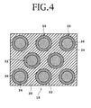
- the nanotube structure film 18 includes an insulator matrix 20 formed of SiO 2 , for example, and a plurality of nanotubes 22 dispersively arranged in the insulator matrix 20.
- Each nanotube 22 is composed of a circular tubular nonmetal 24 and a circular cylindrical metal 26 surrounded by the circular tubular nonmetal 24.
- the circular tubular nonmetal 24 is formed of carbon, for example, and the circular cylindrical metal is formed of chromium, for example.
- the nanotube structure film 18 is partially etched at its central region so that the top of a part of the nanotubes 22 is exposed. Conduction of charge occurs between the upper electrode layer 30 and the lower electrode layer 16, at this etched region, through the magnetoresistive film 28 and the circular cylindrical metals 26 of the exposed nanotube 22. That is, the circular cylindrical metals 26 of the nanotubes 22 present at the etched region of the nanotube structure film 18 form a contact hole.
- FIG. 3 is an enlarged sectional view of an essential part of the preferred embodiment shown in FIG. 2
- FIG. 4 is a cross section taken along the line IV - IV in FIG. 3
- FIG. 5 is a longitudinal sectional view of each nanotube 22.
- the circular tubular nonmetal 24 of each nanotube 22 has an outer diameter d 1 and an inner diameter d 2
- the circular cylindrical metal 26 of each nanotube 22 has the diameter d 2 .
- Each nanotube 22 has a length 1.
- the magnetoresistive film 28 is connected through the nanotubes 22 to the lower electrode layer 16 at the etched region of the nanotube structure film 18.
- a previously-proposed magnetoresistive sensor 2 shown in FIG. 1 provides an output inversely proportional to the square of the diameter of a portion of the magnetoresistive film 8 formed in contact with the lower electrode layer 4, i.e., the diameter of the contact hole 12.
- the magnetoresistive sensor 14 according to the preferred embodiment shown in FIG. 2 provides an output inversely proportional to the sectional area and number of the circular cylindrical metals 26 formed in contact with the magnetoresistive film 28 and the lower electrode layer 16.
- the diameter of a contact portion between the circular cylindrical metals 26 and the lower electrode layer 16, i.e., the apparent diameter D' of a contact hole, will now be calculated. The following assumptions are used for the calculation.
- FIG. 6a shows a photographic view of Cr-C observed by a transmission electron microscope (Formation of carbon nanotubes and their filling with metallic fibers on ion-emitting field anodes: J. Appl. Phys., 84(3), 1626 (1998)).
- the Cr-C forms a structure in which a circular tubular nonmetal of C surrounds a circular cylindrical metal of Cr, i.e., forms a so-called nanotube.
- FIG. 6b is an enlarged view of a portion denoted by an arrow 34 in FIG. 6a
- FIG. 6c is an enlarged view of a portion denoted by an arrow 36 in FIG. 6a.
- the diameter of the circular cylindrical metal of Cr is about 8 nm.
- a manufacturing method for the magnetoresistive sensor 14 will now be described.
- a Cu film having a thickness of 500 nm as the lower electrode layer 16 is deposited on a substrate (not shown), and a resist pattern is next formed on the Cu film.
- the Cu film is then etched by using the resist pattern as a mask to form the lower electrode layer 16 having a desired shape.
- the plural Cr-C nanotubes 22 each having a length of 30 nm are next formed on the lower electrode layer 16.
- the formation of the nanotubes 22 is carried out in the following manner.
- the substrate on which the lower electrode layer 16 has been formed is placed as an anode in a Pyrex glass chamber. After evacuating the chamber to 1 ⁇ 10 -6 Torr, naphthalene C 10 H 8 and hexacarbonyl chromium Cr(CO) 6 gases are mixed at a given ratio, and the mixture is introduced at a total pressure of 0.06 Torr into the chamber.
- the electrodes are maintained at a given high temperature, e.g., 1100 to 1200°C, and a voltage of 4 to 6 kV is applied between the electrodes to thereby form the nanotubes 22 of Cr-C on the lower electrode layer 16 as the anode.
- an SiO 2 film having a thickness of 50 nm as the insulator matrix 20 is continuously deposited by sputtering.
- a resist pattern is next formed on the SiO 2 film, and the SiO 2 film is next etched by using the resist pattern as a mask to remove an unwanted portion of the SiO 2 film.
- a resist pattern is formed again on the SiO 2 film, and the SiO 2 film is next partially etched by using the resist pattern as a mask to form the nanotube structure film 18 whose central region as a contact hole has a thickness of 10 nm.
- the magnetoresistive film 28 having a thickness of 40 nm is deposited on the nanotube structure film 18 by sputtering.
- the magnetoresistive film 28 includes at least one low-resistance film and at least two ferromagnetic films sandwiching the low-resistance film.
- the magnetoresistive film 28 has a ferromagnetic tunnel junction structure or a multilayer film structure composed of a ferromagnetic layer and a nonmagnetic layer.
- the magnetoresistive film 28 may be provided by a spin valve GMR film such as a NiFe/Cu/NiFe/IrMn multilayer film, a laminated ferri spin valve GMR film such as a NiFe/Cu/CoFeB/Ru/CoFeB/PdPtMn multilayer film, or a tunnel junction type MR film (TMR film) such as a NiFe/Al 2 O 3 /NiFe/PdPtMn multilayer film.
- a spin valve GMR film such as a NiFe/Cu/NiFe/IrMn multilayer film
- a laminated ferri spin valve GMR film such as a NiFe/Cu/CoFeB/Ru/CoFeB/PdPtMn multilayer film
- TMR film tunnel junction type MR film
- a Cu film having a thickness of 300 nm as the upper electrode layer 30 is deposited on the magnetoresistive film 28 by sputtering.
- a resist pattern is next formed on the Cu film, and then the Cu film is etched by using the resist pattern as a mask to form the upper electrode layer 30 having a desired shape.
- the magnetoresistive sensor 14 is completed.
- a magnetoresistive sensor as a comparison was fabricated in the following manner.
- a plurality of Cr-C nanotubes each having a length of 10 nm were formed on a lower electrode layer.
- an SiO 2 film having a thickness of 30 nm was deposited on the lower electrode layer so as to fully cover the nanotubes, thus forming a nanotube structure film.
- the nanotube structure film was not etched, and a magnetoresistive film and an upper electrode layer were sequentially deposited on the nanotube structure film.
- the resistance was measured by a DC four-terminal method.
- Table 1 shows the results of measuring the output and resistance of the structure embodying the present invention, the MR sensor fabricated for comparison with the latter, and a previously-proposed magnetoresistive sensor having a CPP structure. Measurement of the output was done by means of a normal four-terminal method, using a 2 mA current and application of a 10 5 A/m magnetic field. Resistance ( ⁇ cm) Output (mV) Structure embodying present Invention 10 nm long Cr-C nanotubes and a 10 nm thick SiO 2 film were used as the contact hole in the magnetoresistive sensor.
- an output of 10 mV is obtained from the magnetoresistive sensor embodying the present invention, and an output of 1 mV is obtained from the previously-proposed magnetoresistive sensor. That is, the output from the embodiment of the present invention is 10 times the output from the previous proposal. Accordingly, it is confirmed that the nanotube structure film according to an embodiment of the present invention can reduce the diameter of the contact hole and can improve the output.
- the output from the comparison is zero for the reason that all the nanotubes as the contact hole are fully embedded in the SiO 2 film, so that no conduction can occur between the magnetoresistive film 28 and the lower electrode layer 16.
- the number of nanotubes functioning as the contact hole in the nanotube structure film in this preferred embodiment will now be calculated.
- the diameter of the contact hole in the prior art magnetoresistive sensor is 0.2 ⁇ m. Therefore, the apparent diameter D' of the contact hole in the magnetoresistive sensor embodying the present invention, whose output is 10 times that of the previous proposal magnetoresistive sensor, becomes 0.2 ⁇ 1/10 1/2 ⁇ 0.063 ⁇ m. Assuming that the diameter of the circular cylindrical metal 26 of each nanotube 22 is 8 nm, the number n of the nanotubes 22 as the contact hole is estimated to be 0.063 2 /0.008 2 ⁇ 62.
- a magnetoresistive sensor having a CPP structure with an improved output and in which the apparent diameter of a contact hole can be reduced. Furthermore, by considering the conditions of formation of the nanotube structure film, the size and number of effective nanotubes as a contact hole can be controlled.
Landscapes
- Engineering & Computer Science (AREA)
- Nanotechnology (AREA)
- Chemical & Material Sciences (AREA)
- Physics & Mathematics (AREA)
- Manufacturing & Machinery (AREA)
- Crystallography & Structural Chemistry (AREA)
- General Physics & Mathematics (AREA)
- Condensed Matter Physics & Semiconductors (AREA)
- Mathematical Physics (AREA)
- Theoretical Computer Science (AREA)
- Hall/Mr Elements (AREA)
- Measuring Magnetic Variables (AREA)
- Magnetic Heads (AREA)
- Internal Circuitry In Semiconductor Integrated Circuit Devices (AREA)
Claims (13)
- Magnetoresistiver Sensor, enthaltend:dadurch gekennzeichnet:obere und untere Elektrodenschichten (30, 16);eine Leitungspfadschicht (18), die zwischen den oberen und unteren Elektrodenschichten vorgesehen ist; undeinen magnetoresistiven Film (28), der zwischen der Leitungspfadschicht und der oberen oder unteren Elektrodenschicht vorgesehen ist;dass die Leitungspfadschicht durch Anordnen eines Zylinders (22) in einem Isolator (20) gebildet ist, welcher Zylinder ein rohrartiges Nichtmetall (24) und ein zylindrisches Metall (26) enthält, das von dem rohrartigen Nichtmetall umgeben ist.
- Magnetoresistiver Sensor nach Anspruch 1, wobei:die Leitungspfadschicht (18) eine erste Region und eine zweite Region hat, die in der Filmdicke kleiner als die erste Region ist.
- Magnetoresistiver Sensor nach Anspruch 1 oder 2, wobei das rohrartige Nichtmetall (24) aus einem Material gebildet ist, das von jenem des Isolators (20) verschieden ist.
- Magnetoresistiver Sensor nach Anspruch 3, wobei das rohrartige Nichtmetall Kohlenstoff enthält.
- Magnetoresistiver Sensor nach einem der vorhergehenden Ansprüche, wobei das zylindrische Metall (26) Chrom enthält.
- Magnetoresistiver Sensor nach einem der vorhergehenden Ansprüche, wobei der Isolator (20) aus SiO2 gebildet ist.
- Magnetoresistiver Sensor nach einem der vorhergehenden Ansprüche, wobei:die Leitungspfadschicht (18) an der unteren Elektrodenschicht (16) vorgesehen ist;der magnetoresistive Film (28) an der Leitungspfadschicht vorgesehen ist;die obere Elektrodenschicht (30) an dem magnetoresistiven Film vorgesehen ist;die Leitungspfadschicht eine Isolatormatrix und eine Mehrzahl von Nanoröhren enthält, die dispersiv in der Isolatormatrix angeordnet sind;jede der Nanoröhren ein kreisartiges rohrartiges Nichtmetall (24) und ein kreisartiges zylindrisches Metall (26) enthält, das von dem kreisartigen rohrartigen Nichtmetall umgeben ist; unddie Leitungspfadschicht teilweise in einer zentralen Region davon geätzt ist, um eine Leitung der oberen Elektrodenschicht und der unteren Elektrodenschicht durch den magnetoresistiven Film und das kreisartige zylindrische Metall jeder Nanoröhre in der zentralen Region herzustellen.
- Magnetoresistiver Sensor nach Anspruch 7, wobei das kreisartige rohrartige Nichtmetall aus Kohlenstoff gebildet ist und das kreisartige zylindrische Metall aus Chrom gebildet ist.
- Magnetoresistiver Sensor nach Anspruch 7 oder 8, wobei die Isolatormatrix aus SiO2 gebildet ist.
- Herstellungsverfahren für einen magnetoresistiven Sensor, enthaltend die Schritte:Ablagern einer unteren Elektrodenschicht (16) auf einem Substrat;Bilden eines zylindrischen Metalls (26), das von einem rohrartigen Nichtmetall (24) umgeben ist, auf der unteren Elektrodenschicht;Ablagern eines Isolators (18) auf der unteren Elektrodenschicht nach dem Bilden des zylindrischen Metalls und des rohrartigen Nichtmetalls, so dass das zylindrische Metall in dem Isolator eingebettet ist, um dadurch eine Leitungspfadschicht zu bilden;Ablagern eines magnetoresistiven Films (28) auf der Leitungspfadschicht; undAblagern einer oberen Elektrodenschicht (30) auf dem magnetoresistiven Film.
- Herstellungsverfahren nach Anspruch 10, ferner enthaltend die Schritte des Bildens eines Resistmusters auf der Leitungspfadschicht, bevor der magnetoresistive Film abgelagert wird; und
teilweises Ätzen der Leitungspfadschicht durch Verwendung des Resistmusters als eine Maske. - Herstellungsverfahren für einen magnetoresistiven Sensor nach Anspruch 10, enthaltend die Schritte:Bilden eines ersten Resistmusters auf der unteren Elektrodenschicht;Ätzen der unteren Elektrodenschicht unter Verwendung des ersten Resistmusters als eine Maske, um die untere Elektrodenschicht in einer gewünschten Form zu bilden;welcher Schritt des Bildens ein Bilden einer Mehrzahl von Nanoröhren aus Cr-C auf der unteren Elektrodenschicht enthält;welcher Schritt des Ablagerns eines Isolators ein Ablagern einer Isolatormatrix auf der unteren Elektrodenschicht enthält, so dass die Mehrzahl von Nanoröhren in der Isolatormatrix eingebetet sind, um einen Nanoröhrenstrukturfilm zu bilden;Bilden eines zweiten Resistmusters auf dem Nanoröhrenstrukturfilm;Ätzen des Nanoröhrenstrukturfilms unter Verwendung des zweiten Resistmusters als eine Maske, um einen unerwünschten Teil des Nanoröhrenstrukturfilms zu entfernen;Bilden eines dritten Resistmusters auf dem Nanoröhrenstrukturfilm;Ätzen einer zentralen Region des Nanoröhrenstrukturfilms unter Verwendung des dritten Resistmuster als eine Maske, so dass die Oberseite jeder Nanoröhre frei liegt, die in der zentralen Region vorhanden ist;welcher Schritt des Ablagerns eines magnetoresistiven Films ein Ablagern eines magnetoresistiven Films auf dem Nanoröhrenstrukturfilm enthält;Bilden eines vierten Resistmusters auf der oberen Elektrodenschicht; undÄtzen der oberen Elektrodenschicht unter Verwendung des vierten Resistmusters als eine Maske, um die obere Elektrodenschicht in einer gewünschten Form zu bilden.
- Herstellungsverfahren nach Anspruch 12, wobei jede Nanoröhre eine kreisartige Röhre, die aus C gebildet ist, und einen kreisartigen Zylinder enthält, der aus Cr gebildet ist, welcher kreisartige Zylinder von der rohrartigen Röhre umgeben ist.
Applications Claiming Priority (2)
| Application Number | Priority Date | Filing Date | Title |
|---|---|---|---|
| JP2001339416 | 2001-11-05 | ||
| JP2001339416A JP2003142755A (ja) | 2001-11-05 | 2001-11-05 | 磁気抵抗センサ及びその製造方法 |
Publications (2)
| Publication Number | Publication Date |
|---|---|
| EP1308741A1 EP1308741A1 (de) | 2003-05-07 |
| EP1308741B1 true EP1308741B1 (de) | 2005-02-02 |
Family
ID=19153765
Family Applications (1)
| Application Number | Title | Priority Date | Filing Date |
|---|---|---|---|
| EP02251657A Expired - Lifetime EP1308741B1 (de) | 2001-11-05 | 2002-03-08 | Magnetoresistiver Sensor und sein Herstellungsverfahren |
Country Status (6)
| Country | Link |
|---|---|
| US (1) | US6828039B2 (de) |
| EP (1) | EP1308741B1 (de) |
| JP (1) | JP2003142755A (de) |
| KR (1) | KR100797590B1 (de) |
| CN (1) | CN1223999C (de) |
| DE (1) | DE60202826T2 (de) |
Families Citing this family (27)
| Publication number | Priority date | Publication date | Assignee | Title |
|---|---|---|---|---|
| US8021976B2 (en) | 2002-10-15 | 2011-09-20 | Megica Corporation | Method of wire bonding over active area of a semiconductor circuit |
| US6937447B2 (en) * | 2001-09-19 | 2005-08-30 | Kabushiki Kaisha Toshiba | Magnetoresistance effect element, its manufacturing method, magnetic reproducing element and magnetic memory |
| WO2003083838A1 (en) * | 2002-03-28 | 2003-10-09 | Fujitsu Limited | Magnetoresistance sensor and method for producing the same |
| JP2004031545A (ja) * | 2002-06-25 | 2004-01-29 | Alps Electric Co Ltd | 磁気検出素子及びその製造方法 |
| US7288845B2 (en) * | 2002-10-15 | 2007-10-30 | Marvell Semiconductor, Inc. | Fabrication of wire bond pads over underlying active devices, passive devices and/or dielectric layers in integrated circuits |
| US7045069B2 (en) * | 2002-11-14 | 2006-05-16 | Gennady Ozeryansky | Microfabrication method based on metal matrix composite technology |
| US7466523B1 (en) * | 2003-07-10 | 2008-12-16 | Yingjian Chen | Nanotube spin valve and method of producing the same |
| JP4689218B2 (ja) * | 2003-09-12 | 2011-05-25 | 株式会社半導体エネルギー研究所 | 半導体装置の作製方法 |
| DE10345755B4 (de) * | 2003-09-25 | 2006-08-31 | Leibniz-Institut Für Festkörper- Und Werkstoffforschung Dresden E.V. | Verfahren zur Herstellung von strukturierten magnetischen Funktionselementen |
| JP2005305634A (ja) * | 2004-03-26 | 2005-11-04 | Fujitsu Ltd | ナノホール構造体及びその製造方法、スタンパ及びその製造方法、磁気記録媒体及びその製造方法、並びに、磁気記録装置及び磁気記録方法 |
| US7194912B2 (en) * | 2004-07-13 | 2007-03-27 | United States Of America As Represented By The Administrator Of The National Aeronautics And Space Administration | Carbon nanotube-based sensor and method for continually sensing changes in a structure |
| TW200631111A (en) * | 2004-11-04 | 2006-09-01 | Koninkl Philips Electronics Nv | Nanotube-based circuit connection approach |
| KR100663881B1 (ko) * | 2005-03-30 | 2007-01-03 | 한국과학기술연구원 | 나노 크기의 수직 전류 인가 메모리 소자 및 그 제조 방법 |
| JP2007299880A (ja) | 2006-04-28 | 2007-11-15 | Toshiba Corp | 磁気抵抗効果素子,および磁気抵抗効果素子の製造方法 |
| US7914915B2 (en) * | 2007-03-06 | 2011-03-29 | The United States of America as represented by the Secretary of the Commerce, The National Institutes of Standards and Technology | Highly charged ion modified oxide device and method of making same |
| JP4388093B2 (ja) * | 2007-03-27 | 2009-12-24 | 株式会社東芝 | 磁気抵抗効果素子、磁気ヘッド、磁気記録再生装置 |
| WO2009050945A1 (ja) * | 2007-10-15 | 2009-04-23 | Fuji Electric Holdings Co., Ltd. | スピンバルブ素子 |
| US7872564B2 (en) * | 2007-11-16 | 2011-01-18 | Infineon Technologies Ag | Integrated lateral short circuit for a beneficial modification of current distribution structure for xMR magnetoresistive sensors |
| JP5039006B2 (ja) | 2008-09-26 | 2012-10-03 | 株式会社東芝 | 磁気抵抗効果素子の製造方法、磁気抵抗効果素子、磁気ヘッドアセンブリ及び磁気記録再生装置 |
| JP5039007B2 (ja) | 2008-09-26 | 2012-10-03 | 株式会社東芝 | 磁気抵抗効果素子の製造方法、磁気抵抗効果素子、磁気ヘッドアセンブリ及び磁気記録再生装置 |
| JP5636654B2 (ja) * | 2009-09-07 | 2014-12-10 | 富士通株式会社 | カーボンナノチューブシート構造体およびその製造方法、半導体装置 |
| CA2784997C (en) * | 2009-12-30 | 2018-06-19 | Jacques Beauvais | Carbon nanotubes based sensing elements and system for monitoring and mapping force, strain and stress |
| US8829901B2 (en) * | 2011-11-04 | 2014-09-09 | Honeywell International Inc. | Method of using a magnetoresistive sensor in second harmonic detection mode for sensing weak magnetic fields |
| US9666790B2 (en) * | 2015-07-17 | 2017-05-30 | Taiwan Semiconductor Manufacturing Co., Ltd. | Manufacturing techniques and corresponding devices for magnetic tunnel junction devices |
| CN105161614A (zh) * | 2015-09-07 | 2015-12-16 | 华中科技大学 | 一种磁隧道结纳米单元结构及其制备方法 |
| CN112750943A (zh) * | 2019-10-30 | 2021-05-04 | 上海磁宇信息科技有限公司 | 磁性隧道结结构及制作方法 |
| CN115602199A (zh) * | 2022-09-27 | 2023-01-13 | 深圳清华大学研究院(Cn) | 硬盘磁头及其制备方法和硬盘 |
Family Cites Families (5)
| Publication number | Priority date | Publication date | Assignee | Title |
|---|---|---|---|---|
| JP2546114B2 (ja) * | 1992-12-22 | 1996-10-23 | 日本電気株式会社 | 異物質内包カーボンナノチューブとその製造方法 |
| DE69926341T2 (de) * | 1999-05-10 | 2006-01-12 | Hitachi Europe Ltd., Maidenhead | Magnetoelektrischer Vorrichtung |
| JP2001143227A (ja) * | 1999-11-18 | 2001-05-25 | Fujitsu Ltd | 磁気センサ |
| US6560077B2 (en) * | 2000-01-10 | 2003-05-06 | The University Of Alabama | CPP spin-valve device |
| US20020145826A1 (en) * | 2001-04-09 | 2002-10-10 | University Of Alabama | Method for the preparation of nanometer scale particle arrays and the particle arrays prepared thereby |
-
2001
- 2001-11-05 JP JP2001339416A patent/JP2003142755A/ja active Pending
-
2002
- 2002-03-08 DE DE60202826T patent/DE60202826T2/de not_active Expired - Lifetime
- 2002-03-08 EP EP02251657A patent/EP1308741B1/de not_active Expired - Lifetime
- 2002-03-13 US US10/097,211 patent/US6828039B2/en not_active Expired - Fee Related
- 2002-03-13 KR KR1020020013493A patent/KR100797590B1/ko not_active Expired - Fee Related
- 2002-04-10 CN CNB021058016A patent/CN1223999C/zh not_active Expired - Fee Related
Also Published As
| Publication number | Publication date |
|---|---|
| US6828039B2 (en) | 2004-12-07 |
| DE60202826T2 (de) | 2006-01-05 |
| KR20030038302A (ko) | 2003-05-16 |
| US20030087130A1 (en) | 2003-05-08 |
| DE60202826D1 (de) | 2005-03-10 |
| CN1223999C (zh) | 2005-10-19 |
| JP2003142755A (ja) | 2003-05-16 |
| KR100797590B1 (ko) | 2008-01-24 |
| CN1417774A (zh) | 2003-05-14 |
| EP1308741A1 (de) | 2003-05-07 |
Similar Documents
| Publication | Publication Date | Title |
|---|---|---|
| US6828039B2 (en) | Magnetoresistive sensor and manufacturing method therefor | |
| US7476954B2 (en) | TMR device with Hf based seed layer | |
| EP1885006B1 (de) | Neue Deckschicht für eine Magnettunnelübergangsvorrichtung zur Verstärkung von dR/R und Herstellungsverfahren dafür | |
| EP1607980B1 (de) | Neue Abdeckstruktur zum Verbessern von dR/R einer MTJ-Vorrichtung | |
| KR100643067B1 (ko) | Cpp 스핀 밸브 소자 | |
| US7016168B2 (en) | Method of increasing CPP GMR in a spin valve structure | |
| US20040246631A1 (en) | Spin valve magnetoresistive device with enhanced performance | |
| JP2000099922A (ja) | 磁気トンネル素子及びその製造方法 | |
| JP2001143227A (ja) | 磁気センサ | |
| US6721148B2 (en) | Magnetoresistive sensor, thin-film read/write head, and magnetic recording apparatus using the sensor | |
| US6441611B2 (en) | Magnetic sensor having a GMR layer | |
| JP3382866B2 (ja) | 磁気抵抗効果素子の製造方法 | |
| US7215515B2 (en) | Magnetoresistive sensor having a conducting path layer formed from a plurality of metal islands within an insulating matrix | |
| EP1424688A2 (de) | Spinventilkopf und Magnetaufzeichnungsvorrichtung hierfür | |
| JP2001102658A (ja) | 磁気抵抗素子 | |
| EP1098203A2 (de) | Bauteil mit magnetischem Tunnelkontakt, magnetoresistiver Kopf mit Tunneleffekt und Herstellungsverfahren | |
| JP2000077744A (ja) | 強磁性トンネル接合磁気抵抗効果素子の製造方法 | |
| JP2004207366A (ja) | Cpp磁気抵抗効果素子及びその製造方法、cpp磁気抵抗効果素子を備えた磁気記憶装置 | |
| JP2003198006A (ja) | 磁気抵抗効果素子 | |
| KR20050053662A (ko) | 자기 저항 헤드 |
Legal Events
| Date | Code | Title | Description |
|---|---|---|---|
| PUAI | Public reference made under article 153(3) epc to a published international application that has entered the european phase |
Free format text: ORIGINAL CODE: 0009012 |
|
| AK | Designated contracting states |
Designated state(s): AT BE CH CY DE DK ES FI FR GB GR IE IT LI LU MC NL PT SE TR |
|
| AX | Request for extension of the european patent |
Extension state: AL LT LV MK RO SI |
|
| 17P | Request for examination filed |
Effective date: 20030602 |
|
| 17Q | First examination report despatched |
Effective date: 20031006 |
|
| AKX | Designation fees paid |
Designated state(s): DE FR GB |
|
| GRAP | Despatch of communication of intention to grant a patent |
Free format text: ORIGINAL CODE: EPIDOSNIGR1 |
|
| GRAS | Grant fee paid |
Free format text: ORIGINAL CODE: EPIDOSNIGR3 |
|
| GRAA | (expected) grant |
Free format text: ORIGINAL CODE: 0009210 |
|
| AK | Designated contracting states |
Kind code of ref document: B1 Designated state(s): DE FR GB |
|
| REG | Reference to a national code |
Ref country code: GB Ref legal event code: FG4D |
|
| REG | Reference to a national code |
Ref country code: IE Ref legal event code: FG4D |
|
| REF | Corresponds to: |
Ref document number: 60202826 Country of ref document: DE Date of ref document: 20050310 Kind code of ref document: P |
|
| PLBE | No opposition filed within time limit |
Free format text: ORIGINAL CODE: 0009261 |
|
| STAA | Information on the status of an ep patent application or granted ep patent |
Free format text: STATUS: NO OPPOSITION FILED WITHIN TIME LIMIT |
|
| ET | Fr: translation filed | ||
| 26N | No opposition filed |
Effective date: 20051103 |
|
| PGFP | Annual fee paid to national office [announced via postgrant information from national office to epo] |
Ref country code: FR Payment date: 20110317 Year of fee payment: 10 |
|
| PGFP | Annual fee paid to national office [announced via postgrant information from national office to epo] |
Ref country code: GB Payment date: 20110302 Year of fee payment: 10 Ref country code: DE Payment date: 20110302 Year of fee payment: 10 |
|
| GBPC | Gb: european patent ceased through non-payment of renewal fee |
Effective date: 20120308 |
|
| REG | Reference to a national code |
Ref country code: FR Ref legal event code: ST Effective date: 20121130 |
|
| REG | Reference to a national code |
Ref country code: DE Ref legal event code: R119 Ref document number: 60202826 Country of ref document: DE Effective date: 20121002 |
|
| PG25 | Lapsed in a contracting state [announced via postgrant information from national office to epo] |
Ref country code: FR Free format text: LAPSE BECAUSE OF NON-PAYMENT OF DUE FEES Effective date: 20120402 Ref country code: GB Free format text: LAPSE BECAUSE OF NON-PAYMENT OF DUE FEES Effective date: 20120308 |
|
| PG25 | Lapsed in a contracting state [announced via postgrant information from national office to epo] |
Ref country code: DE Free format text: LAPSE BECAUSE OF NON-PAYMENT OF DUE FEES Effective date: 20121002 |