EP1307923B1 - Hochvolt-diode und verfahren zu deren herstellung - Google Patents
Hochvolt-diode und verfahren zu deren herstellung Download PDFInfo
- Publication number
- EP1307923B1 EP1307923B1 EP01964927A EP01964927A EP1307923B1 EP 1307923 B1 EP1307923 B1 EP 1307923B1 EP 01964927 A EP01964927 A EP 01964927A EP 01964927 A EP01964927 A EP 01964927A EP 1307923 B1 EP1307923 B1 EP 1307923B1
- Authority
- EP
- European Patent Office
- Prior art keywords
- semiconductor body
- voltage diode
- conduction type
- carried out
- method step
- Prior art date
- Legal status (The legal status is an assumption and is not a legal conclusion. Google has not performed a legal analysis and makes no representation as to the accuracy of the status listed.)
- Expired - Lifetime
Links
- 238000000034 method Methods 0.000 title claims abstract description 56
- 238000004519 manufacturing process Methods 0.000 title claims abstract description 14
- 238000002161 passivation Methods 0.000 claims abstract description 24
- 229910021417 amorphous silicon Inorganic materials 0.000 claims abstract description 7
- 229910052710 silicon Inorganic materials 0.000 claims description 27
- 239000010703 silicon Substances 0.000 claims description 27
- XUIMIQQOPSSXEZ-UHFFFAOYSA-N Silicon Chemical compound [Si] XUIMIQQOPSSXEZ-UHFFFAOYSA-N 0.000 claims description 26
- 239000004065 semiconductor Substances 0.000 claims description 25
- 238000005530 etching Methods 0.000 claims description 15
- 229910052751 metal Inorganic materials 0.000 claims description 15
- 239000002184 metal Substances 0.000 claims description 15
- 238000001465 metallisation Methods 0.000 claims description 15
- 229910001385 heavy metal Inorganic materials 0.000 claims description 10
- 238000005468 ion implantation Methods 0.000 claims description 10
- 239000002019 doping agent Substances 0.000 claims description 8
- 239000002800 charge carrier Substances 0.000 claims description 6
- 238000009792 diffusion process Methods 0.000 claims description 6
- 229910003481 amorphous carbon Inorganic materials 0.000 claims description 5
- 238000000227 grinding Methods 0.000 claims description 5
- 238000000059 patterning Methods 0.000 claims description 5
- 229910052739 hydrogen Inorganic materials 0.000 claims description 3
- 239000001257 hydrogen Substances 0.000 claims description 3
- 125000004429 atom Chemical group 0.000 claims 5
- 238000010438 heat treatment Methods 0.000 claims 2
- 125000004435 hydrogen atom Chemical class [H]* 0.000 claims 2
- 238000001459 lithography Methods 0.000 claims 1
- 230000003647 oxidation Effects 0.000 claims 1
- 238000007254 oxidation reaction Methods 0.000 claims 1
- 230000000873 masking effect Effects 0.000 abstract description 2
- VYPSYNLAJGMNEJ-UHFFFAOYSA-N Silicium dioxide Chemical compound O=[Si]=O VYPSYNLAJGMNEJ-UHFFFAOYSA-N 0.000 description 32
- 239000000758 substrate Substances 0.000 description 18
- 235000012239 silicon dioxide Nutrition 0.000 description 16
- 239000000377 silicon dioxide Substances 0.000 description 16
- 238000000137 annealing Methods 0.000 description 9
- 238000000151 deposition Methods 0.000 description 8
- 239000000463 material Substances 0.000 description 8
- 235000012431 wafers Nutrition 0.000 description 8
- 229920002120 photoresistant polymer Polymers 0.000 description 6
- 229910000789 Aluminium-silicon alloy Inorganic materials 0.000 description 5
- 230000000903 blocking effect Effects 0.000 description 5
- 230000007547 defect Effects 0.000 description 3
- 239000013078 crystal Substances 0.000 description 2
- 230000007423 decrease Effects 0.000 description 2
- 230000001419 dependent effect Effects 0.000 description 2
- 238000011161 development Methods 0.000 description 2
- 230000018109 developmental process Effects 0.000 description 2
- 230000000694 effects Effects 0.000 description 2
- 230000007774 longterm Effects 0.000 description 2
- 230000005855 radiation Effects 0.000 description 2
- 239000000126 substance Substances 0.000 description 2
- ZOXJGFHDIHLPTG-UHFFFAOYSA-N Boron Chemical compound [B] ZOXJGFHDIHLPTG-UHFFFAOYSA-N 0.000 description 1
- UFHFLCQGNIYNRP-UHFFFAOYSA-N Hydrogen Chemical compound [H][H] UFHFLCQGNIYNRP-UHFFFAOYSA-N 0.000 description 1
- OAICVXFJPJFONN-UHFFFAOYSA-N Phosphorus Chemical compound [P] OAICVXFJPJFONN-UHFFFAOYSA-N 0.000 description 1
- 241001499740 Plantago alpina Species 0.000 description 1
- 229910052581 Si3N4 Inorganic materials 0.000 description 1
- 230000005540 biological transmission Effects 0.000 description 1
- 230000015572 biosynthetic process Effects 0.000 description 1
- 229910052796 boron Inorganic materials 0.000 description 1
- 238000011109 contamination Methods 0.000 description 1
- 230000003247 decreasing effect Effects 0.000 description 1
- 238000007688 edging Methods 0.000 description 1
- 230000005684 electric field Effects 0.000 description 1
- 239000002784 hot electron Substances 0.000 description 1
- 238000002513 implantation Methods 0.000 description 1
- 238000002347 injection Methods 0.000 description 1
- 239000007924 injection Substances 0.000 description 1
- 239000012212 insulator Substances 0.000 description 1
- 238000005457 optimization Methods 0.000 description 1
- 230000003071 parasitic effect Effects 0.000 description 1
- 230000035515 penetration Effects 0.000 description 1
- 229910052698 phosphorus Inorganic materials 0.000 description 1
- 239000011574 phosphorus Substances 0.000 description 1
- 238000000206 photolithography Methods 0.000 description 1
- 230000035945 sensitivity Effects 0.000 description 1
- 150000003376 silicon Chemical class 0.000 description 1
- HQVNEWCFYHHQES-UHFFFAOYSA-N silicon nitride Chemical compound N12[Si]34N5[Si]62N3[Si]51N64 HQVNEWCFYHHQES-UHFFFAOYSA-N 0.000 description 1
- 238000009279 wet oxidation reaction Methods 0.000 description 1
- 238000013316 zoning Methods 0.000 description 1
Images
Classifications
-
- H—ELECTRICITY
- H01—ELECTRIC ELEMENTS
- H01L—SEMICONDUCTOR DEVICES NOT COVERED BY CLASS H10
- H01L29/00—Semiconductor devices specially adapted for rectifying, amplifying, oscillating or switching and having potential barriers; Capacitors or resistors having potential barriers, e.g. a PN-junction depletion layer or carrier concentration layer; Details of semiconductor bodies or of electrodes thereof ; Multistep manufacturing processes therefor
- H01L29/40—Electrodes ; Multistep manufacturing processes therefor
- H01L29/402—Field plates
- H01L29/405—Resistive arrangements, e.g. resistive or semi-insulating field plates
-
- H—ELECTRICITY
- H01—ELECTRIC ELEMENTS
- H01L—SEMICONDUCTOR DEVICES NOT COVERED BY CLASS H10
- H01L29/00—Semiconductor devices specially adapted for rectifying, amplifying, oscillating or switching and having potential barriers; Capacitors or resistors having potential barriers, e.g. a PN-junction depletion layer or carrier concentration layer; Details of semiconductor bodies or of electrodes thereof ; Multistep manufacturing processes therefor
- H01L29/66—Types of semiconductor device ; Multistep manufacturing processes therefor
- H01L29/66007—Multistep manufacturing processes
- H01L29/66075—Multistep manufacturing processes of devices having semiconductor bodies comprising group 14 or group 13/15 materials
- H01L29/66083—Multistep manufacturing processes of devices having semiconductor bodies comprising group 14 or group 13/15 materials the devices being controllable only by variation of the electric current supplied or the electric potential applied, to one or more of the electrodes carrying the current to be rectified, amplified, oscillated or switched, e.g. two-terminal devices
- H01L29/6609—Diodes
- H01L29/66128—Planar diodes
-
- H—ELECTRICITY
- H01—ELECTRIC ELEMENTS
- H01L—SEMICONDUCTOR DEVICES NOT COVERED BY CLASS H10
- H01L29/00—Semiconductor devices specially adapted for rectifying, amplifying, oscillating or switching and having potential barriers; Capacitors or resistors having potential barriers, e.g. a PN-junction depletion layer or carrier concentration layer; Details of semiconductor bodies or of electrodes thereof ; Multistep manufacturing processes therefor
- H01L29/66—Types of semiconductor device ; Multistep manufacturing processes therefor
- H01L29/86—Types of semiconductor device ; Multistep manufacturing processes therefor controllable only by variation of the electric current supplied, or only the electric potential applied, to one or more of the electrodes carrying the current to be rectified, amplified, oscillated or switched
- H01L29/861—Diodes
- H01L29/8611—Planar PN junction diodes
Definitions
- the present invention relates to a high-voltage diode according to the preamble of claim 1 and a method for Producing such a high-voltage diode.
- high-voltage diodes are responsible for higher voltages in particular above about 400V, when used of planar structures with edge terminations of field plates, Field rings, dielectric insulating layers, semi-insulating Covers and varying doping in the edge area Mistake. These measures are taken individually or in Combination applied, where quite, for example, too Field plates, field rings and dielectric insulating layers in common be used.
- EP-A-760 528 discloses a diode with edge termination.
- EP-A-264 564 shows a temperature sensor with chipping stopper.
- EP-B1-0 341 453 is a MOS semiconductor device for high Blocking voltage known in the field plates on different thick insulating layers are arranged. Some of these field plates serve as channel or channel stopper. Such Field plates used as channel stoppers become diodes often by a p-type region in the edge region to the backside potential connected to the diode, although in itself Connection over an n-conducting area would be more advantageous because This reliably prevents a p-channel could. However, for such a connection would be over a n-conductive area in a usual manufacturing process an additional mask step is required.
- So-called chipping stoppers are supposed to be used when sawing a disc in individual chips a spread of crystal defects of prevent the saw edge in the active area of the respective chips. These chipping stoppers are usually made by a Field oxide between the functional edge region of the chip and realized the sawing frame.
- amorphous silicon a-Si
- a-C hydrogen amorphous carbon
- Layers can, with appropriate optimization of the amorphous crystalline Heterojunctions between these layers and the electrically active silicon substrate parasitic effects, such as an increased reverse current or the formation of inversion layers, be avoided.
- semi-insulating can Passivation layers due to their finite density of states actively build up image charges and thus penetrate from the outside Shield foreign cargo as well as its finite specific Conduct conductivity injected charge carriers. All in all thus leads to a semi-insulating passivation a dielectric passivation to a much improved Long-term stability.
- a high-voltage diode for reverse voltages in particular over about 400 V and preferably above about 500 V, which with as low as possible Process complexity and thus fewer photo techniques can be produced and in the edge area easily with a channel stopper to avoid leakage currents and a chipping stopper equipped to limit the expansion of sawing defects can be;
- a method for manufacturing such a high-voltage diode can be created.
- This task is in a high-voltage diode according to the preamble of claim 1 according to the invention by in the Characteristics contained in the characterizing part.
- the specified in the characterizing part of claim 1 Measures (a) and (b) each individually for themselves, one High-voltage diode to allow, with little effort for Masks and adjustment can be made and a channel stopper, Chipping-stopper etc. has.
- the measures (a) and (b) can be advantageously used together. Of course it is also possible, a high-voltage diode to create only one of these measures.
- the high-voltage diode according to the invention may be a Fast switchable diode or else a rectifier and universal diode in different voltage and Current classes act.
- the high-voltage diode can be one or more Field rings dependent on the desired voltage class in have their edge area.
- the semiconductor body of n-type silicon, in a p-type well-shaped zone is introduced.
- n-type silicon body can also be p-type silicon body with an n-type trough-shaped Zone be provided.
- the semiconductor material is not limited to silicon. Instead of silicon, it is also possible, for example, to use SiC or an A III B V semiconductor material.
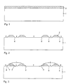
- Fig. 1 shows an n-type silicon substrate 1, to which, for example in a wet oxidation oven process the front side of an approximately 0.5 micron thick silicon dioxide layer. 2 is applied.
- silicon dioxide for this layer 2 also another material, for example Silicon nitride can be selected.
- silicon dioxide layer 2 then structures for the anode of the diode and optionally in the edge region for Field rings introduced by photolithography. This is on the silicon dioxide layer 2 applied a photoresist layer, exposed and developed. In this development, the Areas of the photoresist layer in which the anode and optionally Field rings are to be generated, removed. On the sun Exposed silicon dioxide layer 2 becomes an etchant, for example during a wet-chemical etch, for exposure brought to the silicon dioxide layer in said areas to remove.
- a silicon removal of, for example, 10... 1000 nm, preferably 50 ... 200 nm in the exposed surface of the Silicon substrate 1, ie in the areas of the in the silicon dioxide layer 2 introduced “window” is made.
- This silicon removal can be done over the remaining photoresist or over the remaining after removal of the photoresist silicon dioxide layer 2 be made.
- the in Fig. 2 shown arrangement obtained on the silicon substrate 1 the remaining parts of the silicon dioxide layer 2 and in windows 3 to 5 for an anode (window 3), a Field ring (window 4) and adjustment structures showing in one Ritz frame at the edge of the respective semiconductor chip (in Fig. 2 right margin) (window 5).
- a Field ring can also be provided a plurality of field rings. Possibly can also be dispensed with the field rings.
- the adjustment takes place on adjustment structures forming remaining Edges or steps 6 of the window 5.
- the silicon dioxide layer be further wet-etched back to a wet-chemical certain distance 7 between later in the windows 3 to 5 to be introduced p-type dopants and the edges 6 of the adjustment structures or the step formed thereby in the silicon substrate 1 to produce.
- the remaining photoresist is removed. This is in Fig. 2 (without additional etching back of the silicon substrate) or in Fig. 3 (with additional cognitiveen of the silicon substrate).
- the silicon removal in the windows 3 to 5 made becomes. At least this removal takes place in the window 3, in the area a trough 8 outside of an anode contact 13 (see. below) to create an edge or step as an adjustment structure.
- the arrangement shown in Fig. 2 can thus be generated in the manner be that silicon removal in windows 3 to 5 over the remaining silicon dioxide layer 2 (oxide mask) or over the remaining on this silicon dioxide layer 2 Photoresist takes place.
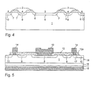
- a p-type doping for example with boron
- a p-type field ring 9 and in the region of the chipping stopper a p-type ring 10, as shown in Fig. 4 are.
- the trough-shaped zone 8 and the field ring 9 and the ring 10 can be produced, for example, in one stage by means of ion implantation or else in multiple stages.
- the edges 6 are used as adjustment structures. It is even possible to make the p-type dopants for the zone 8, the field ring 9 and the ring 10, so the introduction of the front-side p-contact or the p-type emitter with ion implantation at a later date.
- the process variant 1 is special here suitable for base material obtained by zoning (FZ) Silicon substrate disks exists while the process variants 2 and 3 also for Czochralski (CZ-) Substrate wafers or provided with epitaxial layers or diffused wafers are advantageous.
- FZ zoning
- CZ- Czochralski
- the edge passivation layer 12 may optionally also consist of amorphous silicon (a-Si).
- Process variant 1 for: Base material: Si-FZ substrate wafers
- Process variant 2 for: Base material: Si-FZ / CZ substrate wafers or epi- or diffused wafers
- Process variant 3 for: Base material: Si-FZ / CZ substrate disks or epi- or diffused wafers Thin grinding / etching to final thickness Possibly.
- Introduction of heavy metal atoms for carrier lifetime adjustment Possibly.
- Introduction of heavy metal atoms for carrier lifetime adjustment Possibly.
- Irradiation for carrier lifetime adjustment Possibly. Irradiation for carrier lifetime adjustment Possibly. Irradiation for carrier lifetime adjustment Applying the edge passivation, z. From aC: H Applying the edge passivation, z. From aC: H Applying the edge passivation, z. From aC: H Possibly. Irradiation for carrier lifetime adjustment Possibly. Irradiation for carrier lifetime adjustment Possibly. Irradiation for carrier lifetime adjustment Depositing / structuring the front side metallization e.g. B. AlSi Depositing / structuring the front side metallization e.g. B. AlSi Depositing / structuring the front side metallization e.g. B. AlSi Possibly.
- Annealing the front side metallization Possibly. Annealing the front side metallization Possibly. Annealing the front side metallization Possibly. Annealing the front side metallization Possibly. Irradiation for carrier lifetime adjustment Possibly. Irradiation for carrier lifetime adjustment Possibly. Irradiation for carrier lifetime adjustment Thin grinding / etching to final thickness Introduction of an n-doping on the back of the disc as rear-side contact z. B. with ion implantation Depositing backside metal Depositing backside metal Depositing backside metal Possibly. Annealing the backside metal Possibly. Annealing the backside metal Possibly. Annealing the backside metal Possibly. Annealing the backside metal Possibly. Annealing the backside metal Possibly. Annealing the backside metal Possibly. Annealing the backside metal Possibly. Annealing the backside metal
- the particular hydrogen-doped amorphous carbon existing edge passivation layer 12 acts partially as a chipping stopper 12a and prevents the spread from crystal defects starting from a scribe frame into an active one Area when separating or sawing a silicon wafer in chips.
- the passivation layer 12 analogous to the contact holes for the anode contact 13 and the channel stopper 14 is opened, here but no cover made with metal.
- the channel stopper 14 acts as a field plate and prevents the further propagation of a space charge zone to the outside in the Kerf. This makes it possible, the necessary edge width especially with a high-resistance base material for the silicon substrate 1 to reduce.
- the channel stopper 14 may also be provided with a p-type region be connected as indicated by a dashed line 17 in FIG Fig. 5 is indicated. This p-conductive area should then the same electrical potential as the back side of the silicon substrate have, so connected to the cathode contact 15 be.
- channel stopper 14th is directly connected to an n-type region, as in Fig. 5 is shown.
- the field ring 9 may optionally between the active area, ie the trough-shaped zone 8, and a Seederand 18 even more field rings 9 be present, the addition all or partially may be provided with metal structures. Also, the field ring 9 may have such a metal structure.
- the high-voltage diode according to the invention can be thanks to the adjustment structures 6 located outside of the anode contact 13 and the execution of the chipping stopper 12a in FIG Edge area through the passivation layer 12 by means of only a total of three masking steps for the generation of structured silicon dioxide layer 2, the passivation layer 12 and the front side metallization from the anode contact 13 and the channel stopper 14 manufacture.
- the adjustment structure 6 can be utilized be that exact positioning, for example, the anode contact 13 and the channel stopper 14 allowed.
Landscapes
- Engineering & Computer Science (AREA)
- Microelectronics & Electronic Packaging (AREA)
- Power Engineering (AREA)
- Physics & Mathematics (AREA)
- Ceramic Engineering (AREA)
- Condensed Matter Physics & Semiconductors (AREA)
- General Physics & Mathematics (AREA)
- Computer Hardware Design (AREA)
- Manufacturing & Machinery (AREA)
- Electrodes Of Semiconductors (AREA)
Applications Claiming Priority (3)
| Application Number | Priority Date | Filing Date | Title |
|---|---|---|---|
| DE10047152 | 2000-09-22 | ||
| DE10047152A DE10047152B4 (de) | 2000-09-22 | 2000-09-22 | Hochvolt-Diode und Verfahren zu deren Herstellung |
| PCT/DE2001/003240 WO2002025740A1 (de) | 2000-09-22 | 2001-08-24 | Hochvolt-diode und verfahren zu deren herstellung |
Publications (2)
| Publication Number | Publication Date |
|---|---|
| EP1307923A1 EP1307923A1 (de) | 2003-05-07 |
| EP1307923B1 true EP1307923B1 (de) | 2005-11-02 |
Family
ID=7657337
Family Applications (1)
| Application Number | Title | Priority Date | Filing Date |
|---|---|---|---|
| EP01964927A Expired - Lifetime EP1307923B1 (de) | 2000-09-22 | 2001-08-24 | Hochvolt-diode und verfahren zu deren herstellung |
Country Status (5)
| Country | Link |
|---|---|
| US (1) | US6770917B2 (ko) |
| EP (1) | EP1307923B1 (ko) |
| JP (1) | JP2004510333A (ko) |
| DE (2) | DE10047152B4 (ko) |
| WO (1) | WO2002025740A1 (ko) |
Families Citing this family (19)
| Publication number | Priority date | Publication date | Assignee | Title |
|---|---|---|---|---|
| DE10349908C5 (de) * | 2003-10-25 | 2009-02-12 | Semikron Elektronik Gmbh & Co. Kg | Verfahren zur Herstellung eines zweifach passivierten Leistungshalbleiterbauelements mit einer MESA Randstruktur |
| DE102004002908B4 (de) * | 2004-01-20 | 2008-01-24 | Infineon Technologies Ag | Verfahren zum Herstellen eines Halbleiterbauelements oder einer mikromechanischen Struktur |
| DE102006011697B4 (de) * | 2006-03-14 | 2012-01-26 | Infineon Technologies Austria Ag | Integrierte Halbleiterbauelementeanordnung und Verfahren zu deren Herstellung |
| US7538412B2 (en) * | 2006-06-30 | 2009-05-26 | Infineon Technologies Austria Ag | Semiconductor device with a field stop zone |
| JP2008177296A (ja) * | 2007-01-17 | 2008-07-31 | Toyota Central R&D Labs Inc | 半導体装置、pnダイオード、igbt、及びそれらの製造方法 |
| EP2081233A1 (de) * | 2007-12-21 | 2009-07-22 | SEMIKRON Elektronik GmbH & Co. KG | Leistungsdiode mit grabenförmigen Anodenkontaktbereich |
| DE102007062305B3 (de) | 2007-12-21 | 2009-05-28 | Semikron Elektronik Gmbh & Co. Kg | Leistungshalbleiterbauelement mit grabenförmiger Feldringstruktur und Herstellungsverfahren hierzu |
| US7897471B2 (en) * | 2008-06-19 | 2011-03-01 | Fairchild Semiconductor Corporation | Method and apparatus to improve the reliability of the breakdown voltage in high voltage devices |
| JP2010087196A (ja) * | 2008-09-30 | 2010-04-15 | Panasonic Corp | 半導体装置 |
| US8013340B2 (en) * | 2008-09-30 | 2011-09-06 | Infineon Technologies Ag | Semiconductor device with semiconductor body and method for the production of a semiconductor device |
| US8106487B2 (en) | 2008-12-23 | 2012-01-31 | Pratt & Whitney Rocketdyne, Inc. | Semiconductor device having an inorganic coating layer applied over a junction termination extension |
| JP5515922B2 (ja) * | 2010-03-24 | 2014-06-11 | 富士電機株式会社 | 半導体装置 |
| CN103460386B (zh) * | 2011-04-05 | 2016-06-22 | 三菱电机株式会社 | 半导体装置及其制造方法 |
| US8759935B2 (en) * | 2011-06-03 | 2014-06-24 | Infineon Technologies Austria Ag | Power semiconductor device with high blocking voltage capacity |
| JP5841417B2 (ja) * | 2011-11-30 | 2016-01-13 | 株式会社日立製作所 | 窒化物半導体ダイオード |
| US8884342B2 (en) * | 2012-08-29 | 2014-11-11 | Infineon Technologies Ag | Semiconductor device with a passivation layer |
| JP2018156987A (ja) * | 2017-03-15 | 2018-10-04 | 住友電気工業株式会社 | 半導体装置 |
| CN113594262A (zh) * | 2021-07-14 | 2021-11-02 | 深圳基本半导体有限公司 | 一种快恢复二极管结构及其制造方法 |
| CN114093928B (zh) * | 2021-11-11 | 2023-01-13 | 扬州国宇电子有限公司 | 一种快恢复二极管的铂掺杂方法 |
Family Cites Families (12)
| Publication number | Priority date | Publication date | Assignee | Title |
|---|---|---|---|---|
| US4807641A (en) * | 1982-08-27 | 1989-02-28 | Boehringer Laboratories | Pneumotach and components therefore and combined pulmonary function measuring kit containing the same |
| US4487653A (en) * | 1984-03-19 | 1984-12-11 | Advanced Micro Devices, Inc. | Process for forming and locating buried layers |
| EP0220404B1 (de) * | 1985-09-30 | 1991-02-06 | Siemens Aktiengesellschaft | Verfahren zur Begrenzung von Ausbrüchen beim Sägen einer Halbleiterscheibe |
| EP0264564B1 (de) * | 1986-09-30 | 1992-11-11 | Siemens Aktiengesellschaft | Silizium-Temperatursensor |
| DE58905356D1 (de) * | 1988-05-11 | 1993-09-30 | Siemens Ag | MOS-Halbleiterbauelement für hohe Sperrspannung. |
| EP0381111B1 (de) * | 1989-02-01 | 1995-05-31 | Siemens Aktiengesellschaft | Elektroaktive Passivierschicht |
| EP0400178B1 (de) * | 1989-05-31 | 1994-08-03 | Siemens Aktiengesellschaft | Halbleiterbauelement mit Passivierungsschicht |
| DE4410354C2 (de) * | 1994-03-25 | 1996-02-15 | Semikron Elektronik Gmbh | Leistungshalbleiterbauelement |
| JP3994443B2 (ja) | 1995-05-18 | 2007-10-17 | 三菱電機株式会社 | ダイオード及びその製造方法 |
| DE19531369A1 (de) * | 1995-08-25 | 1997-02-27 | Siemens Ag | Halbleiterbauelement auf Siliciumbasis mit hochsperrendem Randabschluß |
| DE19837944A1 (de) * | 1998-08-21 | 2000-02-24 | Asea Brown Boveri | Verfahren zur Fertigung eines Halbleiterbauelements |
| DE19851461C2 (de) * | 1998-11-09 | 2003-07-31 | Semikron Elektronik Gmbh | Schnelle Leistungsdiode und Verfahren zu ihrer Passivierung |
-
2000
- 2000-09-22 DE DE10047152A patent/DE10047152B4/de not_active Expired - Fee Related
-
2001
- 2001-08-24 EP EP01964927A patent/EP1307923B1/de not_active Expired - Lifetime
- 2001-08-24 WO PCT/DE2001/003240 patent/WO2002025740A1/de active IP Right Grant
- 2001-08-24 JP JP2002529847A patent/JP2004510333A/ja active Pending
- 2001-08-24 DE DE50107925T patent/DE50107925D1/de not_active Expired - Lifetime
-
2003
- 2003-03-24 US US10/395,425 patent/US6770917B2/en not_active Expired - Lifetime
Also Published As
| Publication number | Publication date |
|---|---|
| US20030183900A1 (en) | 2003-10-02 |
| DE10047152A1 (de) | 2002-04-25 |
| JP2004510333A (ja) | 2004-04-02 |
| DE50107925D1 (de) | 2005-12-08 |
| EP1307923A1 (de) | 2003-05-07 |
| US6770917B2 (en) | 2004-08-03 |
| WO2002025740A1 (de) | 2002-03-28 |
| DE10047152B4 (de) | 2006-07-06 |
Similar Documents
| Publication | Publication Date | Title |
|---|---|---|
| EP1307923B1 (de) | Hochvolt-diode und verfahren zu deren herstellung | |
| DE102008048832B4 (de) | Halbleitervorrichtung | |
| DE69614949T2 (de) | Leistungs-Halbleiterbauteil mit isoliertem Graben-Gate | |
| DE69032735T2 (de) | Verfahren zum Herstellen von Hochspannungs- und Niederspannungs-CMOS-Transistoren in einem einzigen integrierten Schaltungs-Chip | |
| DE69332619T2 (de) | Verfahren zur Herstellung von einem Feldeffektbauelement mit einem isolierten Gatter | |
| DE19736981C2 (de) | Halbleitereinrichtung mit hoher Durchbruchsspannung | |
| DE69232461T2 (de) | Verfahren zum herstellen von transistoren mit isoliertem gate unter verwendung von platin zur kontrolle der lebensdauer | |
| DE102017124872B4 (de) | Verfahren zur Herstellung eines IGBT mit dV/dt-Steuerbarkeit | |
| DE10214150B4 (de) | Siliziumkarbidhalbleitervorrichtung und Verfahren zur Herstellung derselben | |
| DE102018215731B4 (de) | Halbleitervorrichtung und Verfahren zum Herstellen derselben | |
| DE4114174A1 (de) | Leistungstransistorbauteil sowie verfahren zu seiner herstellung | |
| DE19710487A1 (de) | Halbleitervorrichtung | |
| DE19523172A1 (de) | Bidirektionaler Thyristor | |
| DE102005039564B4 (de) | Verfahren zum Herstellen eines Halbleiterbauteils | |
| DE102012209429A1 (de) | Leistungshalbleiterbauelement mit hoher spannungsfestigkeit | |
| DE4112905A1 (de) | Leitfaehigkeitsmodulations-mosfet und verfahren zu seiner herstellung | |
| DE102018205274A1 (de) | Halbleitervorrichtung und verfahren zu deren herstellung | |
| DE3883889T2 (de) | Verfahren zur Herstellung lateraler Feld-Effekt-Transistoren mit isolierter Gate. | |
| DE112021002169T5 (de) | Halbleitervorrichtung | |
| DE112020006547T5 (de) | Selbstausgerichtete implantate für siliziumkarbid (sic)-technologien und herstellungsverfahren | |
| DE19750221B4 (de) | Verfahren zu Herstellung eines Halbleiterbauteils mit MOS-Gatesteuerung | |
| DE102004017723A1 (de) | In Rückwärtsrichtung sperrendes Halbleiterbauteil und Verfahren zu seiner Herstellung | |
| DE102005040624A1 (de) | Halbleiterbauteil und Verfahren zu seiner Herstellung | |
| DE102021126018A1 (de) | Halbleitervorrichtung und Verfahren zum Herstellen einer Halbleitervorrichtung | |
| DE102019101304B4 (de) | Leistungshalbleitervorrichtung und Verfahren zum Bilden einer Leistungshalbleitervorrichtung |
Legal Events
| Date | Code | Title | Description |
|---|---|---|---|
| PUAI | Public reference made under article 153(3) epc to a published international application that has entered the european phase |
Free format text: ORIGINAL CODE: 0009012 |
|
| 17P | Request for examination filed |
Effective date: 20030305 |
|
| AK | Designated contracting states |
Designated state(s): AT BE CH CY DE DK ES FI FR GB GR IE IT LI LU MC NL PT SE TR |
|
| AX | Request for extension of the european patent |
Extension state: AL LT LV MK RO SI |
|
| RBV | Designated contracting states (corrected) |
Designated state(s): AT BE CH CY DE FR GB IT LI |
|
| GRAP | Despatch of communication of intention to grant a patent |
Free format text: ORIGINAL CODE: EPIDOSNIGR1 |
|
| RBV | Designated contracting states (corrected) |
Designated state(s): CH DE FR GB IT LI |
|
| GRAS | Grant fee paid |
Free format text: ORIGINAL CODE: EPIDOSNIGR3 |
|
| GRAA | (expected) grant |
Free format text: ORIGINAL CODE: 0009210 |
|
| AK | Designated contracting states |
Kind code of ref document: B1 Designated state(s): CH DE FR GB IT LI |
|
| REG | Reference to a national code |
Ref country code: GB Ref legal event code: FG4D Free format text: NOT ENGLISH |
|
| REG | Reference to a national code |
Ref country code: CH Ref legal event code: EP |
|
| REF | Corresponds to: |
Ref document number: 50107925 Country of ref document: DE Date of ref document: 20051208 Kind code of ref document: P |
|
| RAP2 | Party data changed (patent owner data changed or rights of a patent transferred) |
Owner name: INFINEON TECHNOLOGIES AG |
|
| REG | Reference to a national code |
Ref country code: CH Ref legal event code: NV Representative=s name: INFINEON TECHNOLOGIES SCHWEIZ AG |
|
| GBT | Gb: translation of ep patent filed (gb section 77(6)(a)/1977) |
Effective date: 20060503 |
|
| REG | Reference to a national code |
Ref country code: FR Ref legal event code: TP Ref country code: FR Ref legal event code: CD |
|
| ET | Fr: translation filed | ||
| PGFP | Annual fee paid to national office [announced via postgrant information from national office to epo] |
Ref country code: CH Payment date: 20060815 Year of fee payment: 6 |
|
| PGFP | Annual fee paid to national office [announced via postgrant information from national office to epo] |
Ref country code: GB Payment date: 20060824 Year of fee payment: 6 |
|
| PLBE | No opposition filed within time limit |
Free format text: ORIGINAL CODE: 0009261 |
|
| STAA | Information on the status of an ep patent application or granted ep patent |
Free format text: STATUS: NO OPPOSITION FILED WITHIN TIME LIMIT |
|
| 26N | No opposition filed |
Effective date: 20060803 |
|
| REG | Reference to a national code |
Ref country code: CH Ref legal event code: PL |
|
| GBPC | Gb: european patent ceased through non-payment of renewal fee |
Effective date: 20070824 |
|
| PG25 | Lapsed in a contracting state [announced via postgrant information from national office to epo] |
Ref country code: CH Free format text: LAPSE BECAUSE OF NON-PAYMENT OF DUE FEES Effective date: 20070831 Ref country code: LI Free format text: LAPSE BECAUSE OF NON-PAYMENT OF DUE FEES Effective date: 20070831 |
|
| PG25 | Lapsed in a contracting state [announced via postgrant information from national office to epo] |
Ref country code: GB Free format text: LAPSE BECAUSE OF NON-PAYMENT OF DUE FEES Effective date: 20070824 |
|
| REG | Reference to a national code |
Ref country code: FR Ref legal event code: PLFP Year of fee payment: 16 |
|
| REG | Reference to a national code |
Ref country code: FR Ref legal event code: PLFP Year of fee payment: 17 |
|
| REG | Reference to a national code |
Ref country code: FR Ref legal event code: PLFP Year of fee payment: 18 |
|
| PGFP | Annual fee paid to national office [announced via postgrant information from national office to epo] |
Ref country code: FR Payment date: 20180827 Year of fee payment: 18 Ref country code: IT Payment date: 20180830 Year of fee payment: 18 |
|
| PGFP | Annual fee paid to national office [announced via postgrant information from national office to epo] |
Ref country code: DE Payment date: 20181029 Year of fee payment: 18 |
|
| REG | Reference to a national code |
Ref country code: DE Ref legal event code: R119 Ref document number: 50107925 Country of ref document: DE |
|
| PG25 | Lapsed in a contracting state [announced via postgrant information from national office to epo] |
Ref country code: DE Free format text: LAPSE BECAUSE OF NON-PAYMENT OF DUE FEES Effective date: 20200303 Ref country code: FR Free format text: LAPSE BECAUSE OF NON-PAYMENT OF DUE FEES Effective date: 20190831 |
|
| PG25 | Lapsed in a contracting state [announced via postgrant information from national office to epo] |
Ref country code: IT Free format text: LAPSE BECAUSE OF NON-PAYMENT OF DUE FEES Effective date: 20190824 |