EP1307923B1 - High-voltage diode and method for the production thereof - Google Patents
High-voltage diode and method for the production thereof Download PDFInfo
- Publication number
- EP1307923B1 EP1307923B1 EP01964927A EP01964927A EP1307923B1 EP 1307923 B1 EP1307923 B1 EP 1307923B1 EP 01964927 A EP01964927 A EP 01964927A EP 01964927 A EP01964927 A EP 01964927A EP 1307923 B1 EP1307923 B1 EP 1307923B1
- Authority
- EP
- European Patent Office
- Prior art keywords
- semiconductor body
- voltage diode
- conduction type
- carried out
- method step
- Prior art date
- Legal status (The legal status is an assumption and is not a legal conclusion. Google has not performed a legal analysis and makes no representation as to the accuracy of the status listed.)
- Expired - Lifetime
Links
- 238000000034 method Methods 0.000 title claims abstract description 56
- 238000004519 manufacturing process Methods 0.000 title claims abstract description 14
- 238000002161 passivation Methods 0.000 claims abstract description 24
- 229910021417 amorphous silicon Inorganic materials 0.000 claims abstract description 7
- 229910052710 silicon Inorganic materials 0.000 claims description 27
- 239000010703 silicon Substances 0.000 claims description 27
- XUIMIQQOPSSXEZ-UHFFFAOYSA-N Silicon Chemical compound [Si] XUIMIQQOPSSXEZ-UHFFFAOYSA-N 0.000 claims description 26
- 239000004065 semiconductor Substances 0.000 claims description 25
- 238000005530 etching Methods 0.000 claims description 15
- 229910052751 metal Inorganic materials 0.000 claims description 15
- 239000002184 metal Substances 0.000 claims description 15
- 238000001465 metallisation Methods 0.000 claims description 15
- 229910001385 heavy metal Inorganic materials 0.000 claims description 10
- 238000005468 ion implantation Methods 0.000 claims description 10
- 239000002019 doping agent Substances 0.000 claims description 8
- 239000002800 charge carrier Substances 0.000 claims description 6
- 238000009792 diffusion process Methods 0.000 claims description 6
- 229910003481 amorphous carbon Inorganic materials 0.000 claims description 5
- 238000000227 grinding Methods 0.000 claims description 5
- 238000000059 patterning Methods 0.000 claims description 5
- 229910052739 hydrogen Inorganic materials 0.000 claims description 3
- 239000001257 hydrogen Substances 0.000 claims description 3
- 125000004429 atom Chemical group 0.000 claims 5
- 238000010438 heat treatment Methods 0.000 claims 2
- 125000004435 hydrogen atom Chemical class [H]* 0.000 claims 2
- 238000001459 lithography Methods 0.000 claims 1
- 230000003647 oxidation Effects 0.000 claims 1
- 238000007254 oxidation reaction Methods 0.000 claims 1
- 230000000873 masking effect Effects 0.000 abstract description 2
- VYPSYNLAJGMNEJ-UHFFFAOYSA-N Silicium dioxide Chemical compound O=[Si]=O VYPSYNLAJGMNEJ-UHFFFAOYSA-N 0.000 description 32
- 239000000758 substrate Substances 0.000 description 18
- 235000012239 silicon dioxide Nutrition 0.000 description 16
- 239000000377 silicon dioxide Substances 0.000 description 16
- 238000000137 annealing Methods 0.000 description 9
- 238000000151 deposition Methods 0.000 description 8
- 239000000463 material Substances 0.000 description 8
- 235000012431 wafers Nutrition 0.000 description 8
- 229920002120 photoresistant polymer Polymers 0.000 description 6
- 229910000789 Aluminium-silicon alloy Inorganic materials 0.000 description 5
- 230000000903 blocking effect Effects 0.000 description 5
- 230000007547 defect Effects 0.000 description 3
- 239000013078 crystal Substances 0.000 description 2
- 230000007423 decrease Effects 0.000 description 2
- 230000001419 dependent effect Effects 0.000 description 2
- 238000011161 development Methods 0.000 description 2
- 230000018109 developmental process Effects 0.000 description 2
- 230000000694 effects Effects 0.000 description 2
- 230000007774 longterm Effects 0.000 description 2
- 230000005855 radiation Effects 0.000 description 2
- 239000000126 substance Substances 0.000 description 2
- ZOXJGFHDIHLPTG-UHFFFAOYSA-N Boron Chemical compound [B] ZOXJGFHDIHLPTG-UHFFFAOYSA-N 0.000 description 1
- UFHFLCQGNIYNRP-UHFFFAOYSA-N Hydrogen Chemical compound [H][H] UFHFLCQGNIYNRP-UHFFFAOYSA-N 0.000 description 1
- OAICVXFJPJFONN-UHFFFAOYSA-N Phosphorus Chemical compound [P] OAICVXFJPJFONN-UHFFFAOYSA-N 0.000 description 1
- 241001499740 Plantago alpina Species 0.000 description 1
- 229910052581 Si3N4 Inorganic materials 0.000 description 1
- 230000005540 biological transmission Effects 0.000 description 1
- 230000015572 biosynthetic process Effects 0.000 description 1
- 229910052796 boron Inorganic materials 0.000 description 1
- 238000011109 contamination Methods 0.000 description 1
- 230000003247 decreasing effect Effects 0.000 description 1
- 238000007688 edging Methods 0.000 description 1
- 230000005684 electric field Effects 0.000 description 1
- 239000002784 hot electron Substances 0.000 description 1
- 238000002513 implantation Methods 0.000 description 1
- 238000002347 injection Methods 0.000 description 1
- 239000007924 injection Substances 0.000 description 1
- 239000012212 insulator Substances 0.000 description 1
- 238000005457 optimization Methods 0.000 description 1
- 230000003071 parasitic effect Effects 0.000 description 1
- 230000035515 penetration Effects 0.000 description 1
- 229910052698 phosphorus Inorganic materials 0.000 description 1
- 239000011574 phosphorus Substances 0.000 description 1
- 238000000206 photolithography Methods 0.000 description 1
- 230000035945 sensitivity Effects 0.000 description 1
- 150000003376 silicon Chemical class 0.000 description 1
- HQVNEWCFYHHQES-UHFFFAOYSA-N silicon nitride Chemical compound N12[Si]34N5[Si]62N3[Si]51N64 HQVNEWCFYHHQES-UHFFFAOYSA-N 0.000 description 1
- 238000009279 wet oxidation reaction Methods 0.000 description 1
- 238000013316 zoning Methods 0.000 description 1
Images
Classifications
-
- H—ELECTRICITY
- H01—ELECTRIC ELEMENTS
- H01L—SEMICONDUCTOR DEVICES NOT COVERED BY CLASS H10
- H01L29/00—Semiconductor devices adapted for rectifying, amplifying, oscillating or switching, or capacitors or resistors with at least one potential-jump barrier or surface barrier, e.g. PN junction depletion layer or carrier concentration layer; Details of semiconductor bodies or of electrodes thereof ; Multistep manufacturing processes therefor
- H01L29/40—Electrodes ; Multistep manufacturing processes therefor
- H01L29/402—Field plates
- H01L29/405—Resistive arrangements, e.g. resistive or semi-insulating field plates
-
- H—ELECTRICITY
- H01—ELECTRIC ELEMENTS
- H01L—SEMICONDUCTOR DEVICES NOT COVERED BY CLASS H10
- H01L29/00—Semiconductor devices adapted for rectifying, amplifying, oscillating or switching, or capacitors or resistors with at least one potential-jump barrier or surface barrier, e.g. PN junction depletion layer or carrier concentration layer; Details of semiconductor bodies or of electrodes thereof ; Multistep manufacturing processes therefor
- H01L29/66—Types of semiconductor device ; Multistep manufacturing processes therefor
- H01L29/66007—Multistep manufacturing processes
- H01L29/66075—Multistep manufacturing processes of devices having semiconductor bodies comprising group 14 or group 13/15 materials
- H01L29/66083—Multistep manufacturing processes of devices having semiconductor bodies comprising group 14 or group 13/15 materials the devices being controllable only by variation of the electric current supplied or the electric potential applied, to one or more of the electrodes carrying the current to be rectified, amplified, oscillated or switched, e.g. two-terminal devices
- H01L29/6609—Diodes
- H01L29/66128—Planar diodes
-
- H—ELECTRICITY
- H01—ELECTRIC ELEMENTS
- H01L—SEMICONDUCTOR DEVICES NOT COVERED BY CLASS H10
- H01L29/00—Semiconductor devices adapted for rectifying, amplifying, oscillating or switching, or capacitors or resistors with at least one potential-jump barrier or surface barrier, e.g. PN junction depletion layer or carrier concentration layer; Details of semiconductor bodies or of electrodes thereof ; Multistep manufacturing processes therefor
- H01L29/66—Types of semiconductor device ; Multistep manufacturing processes therefor
- H01L29/86—Types of semiconductor device ; Multistep manufacturing processes therefor controllable only by variation of the electric current supplied, or only the electric potential applied, to one or more of the electrodes carrying the current to be rectified, amplified, oscillated or switched
- H01L29/861—Diodes
- H01L29/8611—Planar PN junction diodes
Definitions
- the present invention relates to a high-voltage diode according to the preamble of claim 1 and a method for Producing such a high-voltage diode.
- high-voltage diodes are responsible for higher voltages in particular above about 400V, when used of planar structures with edge terminations of field plates, Field rings, dielectric insulating layers, semi-insulating Covers and varying doping in the edge area Mistake. These measures are taken individually or in Combination applied, where quite, for example, too Field plates, field rings and dielectric insulating layers in common be used.
- EP-A-760 528 discloses a diode with edge termination.
- EP-A-264 564 shows a temperature sensor with chipping stopper.
- EP-B1-0 341 453 is a MOS semiconductor device for high Blocking voltage known in the field plates on different thick insulating layers are arranged. Some of these field plates serve as channel or channel stopper. Such Field plates used as channel stoppers become diodes often by a p-type region in the edge region to the backside potential connected to the diode, although in itself Connection over an n-conducting area would be more advantageous because This reliably prevents a p-channel could. However, for such a connection would be over a n-conductive area in a usual manufacturing process an additional mask step is required.
- So-called chipping stoppers are supposed to be used when sawing a disc in individual chips a spread of crystal defects of prevent the saw edge in the active area of the respective chips. These chipping stoppers are usually made by a Field oxide between the functional edge region of the chip and realized the sawing frame.
- amorphous silicon a-Si
- a-C hydrogen amorphous carbon
- Layers can, with appropriate optimization of the amorphous crystalline Heterojunctions between these layers and the electrically active silicon substrate parasitic effects, such as an increased reverse current or the formation of inversion layers, be avoided.
- semi-insulating can Passivation layers due to their finite density of states actively build up image charges and thus penetrate from the outside Shield foreign cargo as well as its finite specific Conduct conductivity injected charge carriers. All in all thus leads to a semi-insulating passivation a dielectric passivation to a much improved Long-term stability.
- a high-voltage diode for reverse voltages in particular over about 400 V and preferably above about 500 V, which with as low as possible Process complexity and thus fewer photo techniques can be produced and in the edge area easily with a channel stopper to avoid leakage currents and a chipping stopper equipped to limit the expansion of sawing defects can be;
- a method for manufacturing such a high-voltage diode can be created.
- This task is in a high-voltage diode according to the preamble of claim 1 according to the invention by in the Characteristics contained in the characterizing part.
- the specified in the characterizing part of claim 1 Measures (a) and (b) each individually for themselves, one High-voltage diode to allow, with little effort for Masks and adjustment can be made and a channel stopper, Chipping-stopper etc. has.
- the measures (a) and (b) can be advantageously used together. Of course it is also possible, a high-voltage diode to create only one of these measures.
- the high-voltage diode according to the invention may be a Fast switchable diode or else a rectifier and universal diode in different voltage and Current classes act.
- the high-voltage diode can be one or more Field rings dependent on the desired voltage class in have their edge area.
- the semiconductor body of n-type silicon, in a p-type well-shaped zone is introduced.
- n-type silicon body can also be p-type silicon body with an n-type trough-shaped Zone be provided.
- the semiconductor material is not limited to silicon. Instead of silicon, it is also possible, for example, to use SiC or an A III B V semiconductor material.
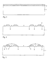
- Fig. 1 shows an n-type silicon substrate 1, to which, for example in a wet oxidation oven process the front side of an approximately 0.5 micron thick silicon dioxide layer. 2 is applied.
- silicon dioxide for this layer 2 also another material, for example Silicon nitride can be selected.
- silicon dioxide layer 2 then structures for the anode of the diode and optionally in the edge region for Field rings introduced by photolithography. This is on the silicon dioxide layer 2 applied a photoresist layer, exposed and developed. In this development, the Areas of the photoresist layer in which the anode and optionally Field rings are to be generated, removed. On the sun Exposed silicon dioxide layer 2 becomes an etchant, for example during a wet-chemical etch, for exposure brought to the silicon dioxide layer in said areas to remove.
- a silicon removal of, for example, 10... 1000 nm, preferably 50 ... 200 nm in the exposed surface of the Silicon substrate 1, ie in the areas of the in the silicon dioxide layer 2 introduced “window” is made.
- This silicon removal can be done over the remaining photoresist or over the remaining after removal of the photoresist silicon dioxide layer 2 be made.
- the in Fig. 2 shown arrangement obtained on the silicon substrate 1 the remaining parts of the silicon dioxide layer 2 and in windows 3 to 5 for an anode (window 3), a Field ring (window 4) and adjustment structures showing in one Ritz frame at the edge of the respective semiconductor chip (in Fig. 2 right margin) (window 5).
- a Field ring can also be provided a plurality of field rings. Possibly can also be dispensed with the field rings.
- the adjustment takes place on adjustment structures forming remaining Edges or steps 6 of the window 5.
- the silicon dioxide layer be further wet-etched back to a wet-chemical certain distance 7 between later in the windows 3 to 5 to be introduced p-type dopants and the edges 6 of the adjustment structures or the step formed thereby in the silicon substrate 1 to produce.
- the remaining photoresist is removed. This is in Fig. 2 (without additional etching back of the silicon substrate) or in Fig. 3 (with additional cognitiveen of the silicon substrate).
- the silicon removal in the windows 3 to 5 made becomes. At least this removal takes place in the window 3, in the area a trough 8 outside of an anode contact 13 (see. below) to create an edge or step as an adjustment structure.
- the arrangement shown in Fig. 2 can thus be generated in the manner be that silicon removal in windows 3 to 5 over the remaining silicon dioxide layer 2 (oxide mask) or over the remaining on this silicon dioxide layer 2 Photoresist takes place.
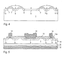
- a p-type doping for example with boron
- a p-type field ring 9 and in the region of the chipping stopper a p-type ring 10, as shown in Fig. 4 are.
- the trough-shaped zone 8 and the field ring 9 and the ring 10 can be produced, for example, in one stage by means of ion implantation or else in multiple stages.
- the edges 6 are used as adjustment structures. It is even possible to make the p-type dopants for the zone 8, the field ring 9 and the ring 10, so the introduction of the front-side p-contact or the p-type emitter with ion implantation at a later date.
- the process variant 1 is special here suitable for base material obtained by zoning (FZ) Silicon substrate disks exists while the process variants 2 and 3 also for Czochralski (CZ-) Substrate wafers or provided with epitaxial layers or diffused wafers are advantageous.
- FZ zoning
- CZ- Czochralski
- the edge passivation layer 12 may optionally also consist of amorphous silicon (a-Si).
- Process variant 1 for: Base material: Si-FZ substrate wafers
- Process variant 2 for: Base material: Si-FZ / CZ substrate wafers or epi- or diffused wafers
- Process variant 3 for: Base material: Si-FZ / CZ substrate disks or epi- or diffused wafers Thin grinding / etching to final thickness Possibly.
- Introduction of heavy metal atoms for carrier lifetime adjustment Possibly.
- Introduction of heavy metal atoms for carrier lifetime adjustment Possibly.
- Irradiation for carrier lifetime adjustment Possibly. Irradiation for carrier lifetime adjustment Possibly. Irradiation for carrier lifetime adjustment Applying the edge passivation, z. From aC: H Applying the edge passivation, z. From aC: H Applying the edge passivation, z. From aC: H Possibly. Irradiation for carrier lifetime adjustment Possibly. Irradiation for carrier lifetime adjustment Possibly. Irradiation for carrier lifetime adjustment Depositing / structuring the front side metallization e.g. B. AlSi Depositing / structuring the front side metallization e.g. B. AlSi Depositing / structuring the front side metallization e.g. B. AlSi Possibly.
- Annealing the front side metallization Possibly. Annealing the front side metallization Possibly. Annealing the front side metallization Possibly. Annealing the front side metallization Possibly. Irradiation for carrier lifetime adjustment Possibly. Irradiation for carrier lifetime adjustment Possibly. Irradiation for carrier lifetime adjustment Thin grinding / etching to final thickness Introduction of an n-doping on the back of the disc as rear-side contact z. B. with ion implantation Depositing backside metal Depositing backside metal Depositing backside metal Possibly. Annealing the backside metal Possibly. Annealing the backside metal Possibly. Annealing the backside metal Possibly. Annealing the backside metal Possibly. Annealing the backside metal Possibly. Annealing the backside metal Possibly. Annealing the backside metal Possibly. Annealing the backside metal
- the particular hydrogen-doped amorphous carbon existing edge passivation layer 12 acts partially as a chipping stopper 12a and prevents the spread from crystal defects starting from a scribe frame into an active one Area when separating or sawing a silicon wafer in chips.
- the passivation layer 12 analogous to the contact holes for the anode contact 13 and the channel stopper 14 is opened, here but no cover made with metal.
- the channel stopper 14 acts as a field plate and prevents the further propagation of a space charge zone to the outside in the Kerf. This makes it possible, the necessary edge width especially with a high-resistance base material for the silicon substrate 1 to reduce.
- the channel stopper 14 may also be provided with a p-type region be connected as indicated by a dashed line 17 in FIG Fig. 5 is indicated. This p-conductive area should then the same electrical potential as the back side of the silicon substrate have, so connected to the cathode contact 15 be.
- channel stopper 14th is directly connected to an n-type region, as in Fig. 5 is shown.
- the field ring 9 may optionally between the active area, ie the trough-shaped zone 8, and a Seederand 18 even more field rings 9 be present, the addition all or partially may be provided with metal structures. Also, the field ring 9 may have such a metal structure.
- the high-voltage diode according to the invention can be thanks to the adjustment structures 6 located outside of the anode contact 13 and the execution of the chipping stopper 12a in FIG Edge area through the passivation layer 12 by means of only a total of three masking steps for the generation of structured silicon dioxide layer 2, the passivation layer 12 and the front side metallization from the anode contact 13 and the channel stopper 14 manufacture.
- the adjustment structure 6 can be utilized be that exact positioning, for example, the anode contact 13 and the channel stopper 14 allowed.
Abstract
Description
Die vorliegende Erfindung betrifft eine Hochvolt-Diode nach
dem Oberbegriff des Patentanspruches 1 sowie ein Verfahren zum
Herstellen einer solchen Hochvolt-Diode.The present invention relates to a high-voltage diode according to
the preamble of
Bisher werden Hochvolt-Dioden, die für höhere Spannungen insbesondere oberhalb von etwa 400 V vorgesehen sind, bei Verwendung von planaren Strukturen mit Randabschlüssen aus Feldplatten, Feldringen, dielektrischen Isolierschichten, semiisolierenden Abdeckungen und variierender Dotierung im Randbereich versehen. Dabei werden diese Maßnahmen einzeln oder in Kombination angewandt, wobei durchaus beispielsweise auch Feldplatten, Feldringe und dielektrische Isolierschichten gemeinsam zum Einsatz kommen.So far, high-voltage diodes are responsible for higher voltages in particular above about 400V, when used of planar structures with edge terminations of field plates, Field rings, dielectric insulating layers, semi-insulating Covers and varying doping in the edge area Mistake. These measures are taken individually or in Combination applied, where quite, for example, too Field plates, field rings and dielectric insulating layers in common be used.
Dabei hat es sich gezeigt, dass bei der Herstellung der Diode für einen den an ihn gestellten Forderungen genügenden Randabschluss sogar mehr Schritte als zur Einstellung der gewünschten Durchlass- und Schalteigenschaften notwendig sind. So erfordern beispielsweise Diodenränder auf der Basis von Feldplatten relativ aufwändige Herstellungsprozesse.It has been shown that in the production of the diode for a sufficient margins for the demands made on him even more steps than to set the desired Passage and switching properties are necessary. For example, diode edges require on the basis of Field plates relatively complex manufacturing processes.
Im Einzelnen sind in C. Mingues und G. Charitat: "Efficiency of Junction Termination Techniques vs. Oxide Trapped Charges", 1997, IEEE International Symposium on Power Semiconductor Devices and ICs, Weimar, Seiten 137 bis 140, Randabschlüsse mit Feldringen, semiisolierenden Schichten oder einer JTE (Junction Termination Extension) speziell hinsichtlich ihrer Empfindlichkeit gegenüber Oxydladungen miteinander verglichen. Dabei werden für Hochspannungsanwendungen als semiisolierende Schichten der Einsatz von SIPOS-Techniken empfohlen.Specifically, in C. Mingues and G. Charitat, "Efficiency of Junction Termination Techniques vs. Oxide Trapped Charges ", 1997, IEEE International Symposium on Power Semiconductor Devices and ICs, Weimar, pages 137 to 140, edging with Field rings, semi-insulating layers or a JTE (Junction Termination Extension) especially with regard to their sensitivity compared to Oxydladungen compared. These are used for high voltage applications as semi-insulating Layers recommended the use of SIPOS techniques.
EP-A-760 528 offenbert eine Diode mit Randabschluß. EP-A- 264 564 zeigt einen Temperatursensor mit Chipping Stopper.EP-A-760 528 discloses a diode with edge termination. EP-A-264 564 shows a temperature sensor with chipping stopper.
Aus EP-B1-0 341 453 ist ein MOS-Halbleiterbauelement für hohe Sperrspannung bekannt, bei dem Feldplatten auf verschieden dicken Isolierschichten angeordnet sind. Einige dieser Feldplatten dienen dabei als Kanal- bzw. Channel-Stopper. Solche als Kanal-Stopper verwendeten Feldplatten werden bei Dioden oft durch ein p-leitendes Gebiet im Randbereich an das Rückseitenpotenzial der Diode angeschlossen, obwohl an sich ein Anschluss über ein n-leitendes Gebiet vorteilhafter wäre, weil dadurch ein p-leitender Kanal zuverlässig verhindert werden könnte. Allerdings wäre für einen solchen Anschluss über ein n-leitendes Gebiet bei einem sonst üblichen Herstellungsprozess ein zusätzlicher Maskenschritt erforderlich.From EP-B1-0 341 453 is a MOS semiconductor device for high Blocking voltage known in the field plates on different thick insulating layers are arranged. Some of these field plates serve as channel or channel stopper. Such Field plates used as channel stoppers become diodes often by a p-type region in the edge region to the backside potential connected to the diode, although in itself Connection over an n-conducting area would be more advantageous because This reliably prevents a p-channel could. However, for such a connection would be over a n-conductive area in a usual manufacturing process an additional mask step is required.
So genannte Chipping-Stopper sollen beim Sägen einer Scheibe in einzelne Chips eine Ausbreitung von Kristalldefekten von der Sägekante in das aktive Gebiet der jeweiligen Chips verhindern. Diese Chipping-Stopper werden üblicherweise durch ein Feldoxid zwischen dem funktionellen Randbereich des Chips und dem Sägerahmen realisiert.So-called chipping stoppers are supposed to be used when sawing a disc in individual chips a spread of crystal defects of prevent the saw edge in the active area of the respective chips. These chipping stoppers are usually made by a Field oxide between the functional edge region of the chip and realized the sawing frame.
Werden hoch sperrende pn-Übergänge nur mit dielektrischen Passivierungsschichten abgedeckt, so können bei Einwirkung von äußeren Ladungen, die beispielsweise auf Feuchtigkeit, alkalische oder metallische Kontamination etc. zurückzuführen sind, bei Sperrbelastung des pn-Überganges Veränderungen in der Langzeit-Sperrstabilität beobachtet werden. Diese Veränderungen werden durch Drift von Ionenladungen im elektrischen Feld des in Sperrrichtung gepolten pn-Überganges auf oder in der Passivierungsschicht hervorgerufen. Abhängig von dem Vorzeichen der Ionenladungen und auch abhängig von der Struktur des Randabschlusses, also abhängig von der so genannten Randkontur, können die Ionenladungen zu einer Erhöhung oder zu einer Erniedrigung der Sperrfähigkeit des pn-Überganges führen. Bei einer Diode mit p-leitender Anode nimmt dabei mit abnehmender Dotierung in der n-leitenden Basis und daher mit zunehmender Volumensperrfähigkeit der Diode durch eine größere Influenzwirkung der Einfluss solcher Oberflächenladungen in und auf der Passivierungsschicht zu, was zu einer dramatischen Steigerung der Gefahr von Sperrinstabilitäten führt. In diesem Zusammenhang ist auf den so genannten Yoshida-Effekt zu verweisen: Bei Einsatz von Isolatorschichten zur Passivierung wird gelegentlich infolge einer Injektion von heißen Elektronen während der Durchlassbelastung beim Umschalten in den Sperrzustand des pn-Überganges eine Drift der Sperrspannung beobachtet.Become high-barrier pn junctions with only dielectric passivation layers covered, so under the influence of external charges, for example, to moisture, alkaline or metallic contamination, etc., at blocking load of the pn junction changes in the Long-term blocking stability can be observed. These changes are caused by drift of ion charges in the electric Field of the reversed poled pn junction on or in the passivation layer caused. Depending on the sign the ion charges and also depending on the structure of the edge termination, thus depending on the so-called edge contour, For example, the ion charges can increase or decrease Lowering the blocking ability of the pn junction lead. With a diode with p-conducting anode thereby decreases with decreasing Doping in the n-type base and therefore with increasing Volume blocking capability of the diode due to a greater influence effect the influence of such surface charges in and on the passivation layer too, resulting in a dramatic Increasing the risk of locking instabilities leads. In this Context is to refer to the so-called Yoshida effect: When using insulator layers for passivation is occasionally due to an injection of hot electrons during the transmission load when switching to the Locked state of the pn junction a drift of reverse voltage observed.
Durch den Einsatz von semiisolierenden Schichten direkt auf den pn-Übergängen kann bei geeigneten Einstellungen der Schicht- und Grenzflächenparameter, wie beispielsweise der Schichtdicke und Dotierung der semiisolierenden Schichten, der Einfluss solcher Oberflächenladungen unterdrückt werden. Die semiisolierenden Schichten, die derzeit zur Passivierung von pn-Übergängen eingesetzt werden, bestehen beispielsweise aus amorphem Silizium (a-Si) oder aus mit Wasserstoff dotier-tem amorphem Kohlenstoff (a-C:H), wie sie in EP-B1-0 400 178 und EP-B1-0 381 111 beschrieben sind. Mit diesen semiisolie-renden Schichten können bei entsprechender Optimierung der amorphkristallinen Heteroübergänge zwischen diesen Schichten und dem elektrisch aktiven Siliziumsubstrat parasitäre Effek-te, wie ein erhöhter Sperrstrom oder die Ausbildung von Inversionsschichten, vermieden werden. Außerdem können semiisolierende Passivierungsschichten durch ihre endliche Zustandsdichte aktiv Bildladungen aufbauen und so von außen eindringende Fremdladungen abschirmen sowie durch ihre endliche spezifische Leitfähigkeit injizierte Ladungsträger ableiten. Insgesamt führt so eine semiisolierende Passivierung gegenüber einer dielektrischen Passivierung zu einer wesentlich verbesserten Langzeitstabilität.By using semi-insulating layers directly on the pn-transitions can be made under suitable settings Layer and interface parameters, such as the Layer thickness and doping of the semi-insulating layers, the Influence of such surface charges are suppressed. The semi-insulating layers currently used for passivation of pn junctions are used, for example amorphous silicon (a-Si) or doped with hydrogen amorphous carbon (a-C: H), as described in EP-B1-0 400 178 and EP-B1-0 381 111 are described. With these semi-insulating ones Layers can, with appropriate optimization of the amorphous crystalline Heterojunctions between these layers and the electrically active silicon substrate parasitic effects, such as an increased reverse current or the formation of inversion layers, be avoided. In addition, semi-insulating can Passivation layers due to their finite density of states actively build up image charges and thus penetrate from the outside Shield foreign cargo as well as its finite specific Conduct conductivity injected charge carriers. All in all thus leads to a semi-insulating passivation a dielectric passivation to a much improved Long-term stability.
Es ist Aufgabe der vorliegenden Erfindung, eine Hochvolt-Diode für Sperrspannungen insbesondere über etwa 400 V und vorzugsweise über etwa 500 V anzugeben, welche mit möglichst geringer Prozesskomplexität und damit geringer Anzahl von Fototechniken herstellbar ist und im Randbereich ohne Weiteres mit einem Kanal-Stopper zur Vermeidung von Leckströmen und einem Chipping-Stopper zur Begrenzung der Ausdehnung von Sägedefekten ausgestattet werden kann; außerdem soll ein Verfahren zum Herstellen einer solchen Hochvolt-Diode geschaffen werden. It is an object of the present invention, a high-voltage diode for reverse voltages in particular over about 400 V and preferably above about 500 V, which with as low as possible Process complexity and thus fewer photo techniques can be produced and in the edge area easily with a channel stopper to avoid leakage currents and a chipping stopper equipped to limit the expansion of sawing defects can be; In addition, a method for manufacturing such a high-voltage diode can be created.
Diese Aufgabe wird bei einer Hochvolt-Diode nach dem Oberbegriff
des Patentanspruches 1 erfindungsgemäß durch die in dessen
kennzeichnendem Teil enthaltenen Merkmale gelöst.This task is in a high-voltage diode according to the preamble
of
Ein vorteilhaftes Verfahren zum Herstellen der erfindungsgemäßen
Hochvolt-Diode ist in Patentanspruch 12 angegeben.An advantageous method for producing the inventive
High-voltage diode is specified in
Vorteilhafte Weiterbildungen der Erfindung ergeben sich aus den Unteransprüchen.Advantageous developments of the invention will become apparent the dependent claims.
Die im kennzeichnenden Teil des Patentanspruches 1 angegebenen
Maßnahmen (a) und (b) dienen jede einzeln für sich dazu, eine
Hochvolt-Diode zu ermöglichen, die mit geringem Aufwand für
Masken und Justage herstellbar ist und über einen Kanal-Stopper,
Chipping-Stopper etc. verfügt. Die Maßnahmen (a) und
(b) können in vorteilhafter Weise gemeinsam angewandt werden.
Selbstverständlich ist es aber auch möglich, eine Hochvolt-Diode
zu schaffen, die nur eine dieser Maßnahmen realisiert.The specified in the characterizing part of
Bei der erfindungsgemäßen Hochvolt-Diode kann es sich um eine schnelle schaltfeste Diode oder aber auch um eine Gleichrichter- und Universal-Diode in verschiedenen Spannungs- und Stromklassen handeln. Die Hochvolt-Diode kann einen oder mehrere Feldringe abhängig von der gewünschten Spannungsklasse in ihrem Randbereich haben.The high-voltage diode according to the invention may be a Fast switchable diode or else a rectifier and universal diode in different voltage and Current classes act. The high-voltage diode can be one or more Field rings dependent on the desired voltage class in have their edge area.
In bevorzugter Weise besteht bei der erfindungsgemäßen Hochvolt-Diode der Halbleiterkörper aus n-leitendem Silizium, in das eine p-leitende wannenförmige Zone eingebracht ist.Preferably, in the high-voltage diode according to the invention the semiconductor body of n-type silicon, in a p-type well-shaped zone is introduced.
Anstelle eines n-leitenden Siliziumkörpers kann aber auch ein p-leitender Siliziumkörper mit einer n-leitenden wannenförmigen Zone vorgesehen werden.But instead of an n-type silicon body can also be p-type silicon body with an n-type trough-shaped Zone be provided.
Das Halbleitermaterial ist nicht auf Silizium begrenzt. Anstelle von Silizium kann beispielsweise auch SiC oder ein AIIIBV-Halbleitermaterial eingesetzt werden. The semiconductor material is not limited to silicon. Instead of silicon, it is also possible, for example, to use SiC or an A III B V semiconductor material.
Nachfolgend wird die Erfindung anhand von Zeichnungen näher erläutert, in deren Fig. 1 bis 5 verschiedene Schritte zur Herstellung der erfindungsgemäßen Hochvolt-Diode dargestellt sind.The invention will be more apparent from the following drawings explained, in whose Fig. 1 to 5 different steps for Production of the high-voltage diode according to the invention shown are.
Fig. 1 zeigt ein n-leitendes Siliziumsubstrat 1, auf das beispielsweise
in einem Ofenprozess mit feuchter Oxidation auf
der Vorderseite eine etwa 0,5 µm dicke Siliziumdioxidschicht 2
aufgebracht wird. Anstelle von Silizumdioxid kann gegebenenfalls
für diese Schicht 2 auch ein anderes Material, beispielsweise
Siliziumnitrid, gewählt werden.Fig. 1 shows an n-
In der Siliziumdioxidschicht 2 werden sodann Strukturen für
die Anode der Diode und gegebenenfalls im Randbereich für
Feldringe mittels Fotolithografie eingebracht. Hierzu wird auf
die Siliziumdioxidschicht 2 eine Fotolackschicht aufgetragen,
belichtet und entwickelt. Bei dieser Entwicklung werden die
Bereiche der Fotolackschicht, in denen die Anode und gegebenenfalls
Feldringe erzeugt werden sollen, entfernt. Auf die so
freiliegende Siliziumdioxidschicht 2 wird ein Ätzmittel, beispielsweise
während einer nasschemischen Ätzung, zur Einwirkung
gebracht, um in den genannten Bereichen die Siliziumdioxidschicht
zu entfernen.In the
Es schließt sich sodann ein weiterer Ätzschritt an, bei welchem
ein Silizium-Abtrag von beispielsweise 10 ... 1000 nm,
vorzugsweise 50 ... 200 nm in der freiliegenden Oberfläche des
Siliziumsubstrates 1, also in den Bereichen der in die Siliziumdioxidschicht
2 eingebrachten "Fenster" vorgenommen wird.
Dieser Silizium-Abtrag kann über den noch vorhandenen Fotolack
oder über die nach Entfernung des Fotolackes verbleibende Siliziumdioxidschicht
2 vorgenommen werden. Damit wird die in
Fig. 2 gezeigte Anordnung erhalten, welche auf dem Siliziumsubstrat
1 die verbleibenden Teile der Siliziumdioxidschicht 2
und in Fenstern 3 bis 5 für eine Anode (Fenster 3), einen
Feldring (Fenster 4) und Justage-Strukturen zeigt, die in einem
Ritzrahmen am Rand des jeweiligen Halbleiterchips (in Fig.
2 rechter Rand) definiert werden (Fenster 5). Anstelle eines
Feldringes können auch mehrere Feldringe vorgesehen sein. Gegebenenfalls
kann auf die Feldringe auch verzichtet werden.
Die Justage erfolgt an Justage-Strukturen bildenden verbleibenden
Kanten oder Stufen 6 des Fensters 5.This is followed by another etching step, in which
a silicon removal of, for example, 10... 1000 nm,
preferably 50 ... 200 nm in the exposed surface of the
Bei der Ätzung des Siliziumsubstrates 1 in den Fenstern 3 bis
5 kann über die noch vorliegende Lackmaske die Siliziumdioxidschicht
weiter nasschemisch zurückgeätzt werden, um einen
gewissen Abstand 7 zwischen später in den Fenstern 3 bis 5
einzubringenden p-Dotierungen und den Kanten 6 der Justage-Strukturen
bzw. der durch diese gebildeten Stufe im Siliziumsubstrat
1 zu erzeugen. Spätestens nach diesem gegebenenfalls
erfolgenden Rückätzen wird der verbleibende Fotolack entfernt.
Damit liegt die in Fig. 2 (ohne zusätzliches Rückätzen des Siliziumsubstrates)
bzw. in Fig. 3 (mit zusätzlichem Rückätzen
des Siliziumsubstrates) gezeigte Anordnung vor.During the etching of the
Es sei noch angemerkt, dass im vorliegenden Ausführungsbeispiel
der Silizium-Abtrag in den Fenstern 3 bis 5 vorgenommen
wird. Zumindest erfolgt dieser Abtrag im Fenster 3, um im Bereich
einer Wanne 8 außerhalb eines Anodenkontaktes 13 (vgl.
unten) eine Kante bzw. Stufe als Justage-Struktur zu erzeugen.It should be noted that in the present embodiment
the silicon removal in the
Die in Fig. 2 gezeigte Anordnung kann also in der Weise erzeugt
werden, dass der Silizium-Abtrag in den Fenstern 3 bis 5
über die verbleibende Siliziumdioxidschicht 2 (Oxidmaske) bzw.
über den auf dieser Siliziumdioxidschicht 2 noch vorhandenen
Fotolack erfolgt.The arrangement shown in Fig. 2 can thus be generated in the manner
be that silicon removal in
Im Folgenden wird davon ausgegangen, dass die Anordnung von
Fig. 3 weiterverarbeitet wird. Es ist jedoch auch möglich, die
Anordnung von Fig. 2 in entsprechender Weise zu verarbeiten.
In diesem Fall ist aber der Abstand 7 zwischen dem Rand der
verbleibenden Siliziumdioxidschicht 2 und den Kanten 6 der Justage-Strukturen
nicht vorhanden. Vielmehr schließen sich diese
Kanten 6 der Justage-Strukturen dann lagemäßig direkt an
den Rand der Fenster 3 bis 5 an. In the following it is assumed that the arrangement of
Fig. 3 is further processed. However, it is also possible that
Arrangement of Fig. 2 to process in a corresponding manner.
In this case, however, the
Es folgt sodann eine p-Dotierung, beispielsweise mit Bor, um
eine p-leitende wannenförmige Zone 8, einen p-leitenden Feldring
9 und im Bereich des Chipping-Stoppers einen p-leitenden
Ring 10 zu erzeugen, wie diese in Fig. 4 dargestellt sind. Die
wannenförmige Zone 8 sowie der Feldring 9 und der Ring 10 können
beispielsweise einstufig mittels Ionenimplantation oder
auch mehrstufig hergestellt werden. So ist es speziell bei
schnell schaltenden Dioden für die Zone 8 möglich, diese mit
einem p+-leitenden Anoden-emitter von geringer Eindringtiefe zu
versehen, dessen Dotierstoff-Dosis zwischen 1,3 x 10¹²Dotierstoff-Atomen
cm-2 und 5 x 10¹³ Dotierstoffatomen cm-2 liegt, und
den Rest der Zone 8 mit einer Dosis von etwa (1,3 ... 3) x 1012
Dotierstoffatomen cm-2 zu dotieren (vgl. hierzu auch DE-A1-100
31 461).It then follows a p-type doping, for example with boron, to produce a p-type well-
Für die Weiterprozessierung der in Fig. 4 gezeigten Anordnung
gibt es nun verschiedene Varianten, bei denen notwendige Prozessschritte,
wie das Einbringen einer n-Dotierung (beispielsweise
Phosphor) auf der Rückseite des Halbleitersubstrates
1, also der Scheibenrückseite, als Rückseiten-Emitter
zur Bildung einer n+-leitenden Siliziumschicht 11 beispielsweise
durch Ionenimplantation, das Abätzen der verbleibenden
Siliziumdioxidschicht 2 (Opferoxid) auf der Scheibenvorderseite,
das Aufbringen und Strukturieren einer Randpassivierungsschicht
12 mit einem Chipping-Stopper 12a aus jeweils
insbesondere mit Wasserstoff dotiertem amorphem Kohlenstoff
(a-C:H) unter Verwendung eines Lithographieschrittes, das Abscheiden
und die Strukturierung einer Vorderseitenmetallisierung
aus beispielsweise AlSi zur Bildung eines Anodenkontaktes
13 und eines Kanal-Stoppers 14 und das Abscheiden einer Rückseitenmetallisierung
aus beispielsweise AlSi zur Bildung eines
Kathodenkontaktes 15 sowie fakultative Prozessschritte, wie
das Dünnschleifen bzw. Ätzen des Siliziumsubstrates 1 von der
Rückseite auf Enddicke, das Einbringen einer n-leitenden Dotierung
als Feldstoppschicht 16 auf der Scheibenrückseite und
Ausdiffusion dieser n-leitenden Dotierung, das Einbringen von
Schwermetallatomen zur Ladungsträgerlebensdauer-Einstellung,
die Schwermetalldiffusion, die Bestrahlung zur Ladungsträgerlebensdauer-Einstellung,
das Tempern der Vorderseitenmetallisierung
und das Tempern des Rückseitenmetalls vorgenommen
werden. Bei diesen Prozeßschritten werden, soweit erforderlich,
die Kanten 6 als Justage-Strukturen verwendet. Dabei
ist es sogar möglich, die p-leitenden Dotierungen für die
Zone 8, den Feldring 9 und den Ring 10, also das Einbringen
des Vorderseiten-p-Kontaktes bzw. des p-leitenden Emitters mit
Ionenimplantation zu einem späteren Zeitpunkt vorzunehmen.For the further processing of the arrangement shown in Fig. 4, there are now various variants in which necessary process steps, such as the introduction of an n-type doping (for example phosphorus) on the back of the semiconductor substrate 1, ie the back of the disc, as a backside emitter to form a n + -type silicon layer 11, for example, by ion implantation, etching the remaining silicon dioxide layer 2 (sacrificial oxide) on the wafer front side, applying and structuring an edge passivation layer 12 with a chipping stopper 12a, in particular hydrogen-doped amorphous carbon (aC: H) Use of a lithographic step, depositing and patterning a front side metallization of, for example, AlSi to form an anode contact 13 and a channel stopper 14 and depositing a backside metallization of, for example, AlSi to form a cathode contact 15, and optionally Process steps, such as the thin grinding or etching of the silicon substrate 1 from the back to final thickness, the introduction of an n-type doping as a field stop layer 16 on the back of the disc and out diffusion of this n-type doping, the introduction of heavy metal atoms for carrier lifetime adjustment, the heavy metal diffusion , irradiation for carrier lifetime adjustment, annealing of the front surface metallization, and annealing of the back metal are performed. In these process steps, if necessary, the
Diese einzelnen Prozessvarianten sind in der folgenden Tabelle
zusammengestellt. Dabei ist die Prozessvariante 1 besonders
für Grundmaterial geeignet, das aus durch Zonenziehen (FZ) erhaltenen
Silizium-Substratscheiben besteht, während die Prozessvarianten
2 und 3 auch für Czochralski-(CZ-)
Substratscheiben oder für mit epitaktischen Schichten versehene
bzw. diffundierte ("diffused") Wafer vorteilhaft sind.These individual process variants are in the following table
compiled. The
Die Randpassivierungsschicht 12 (und damit der Chipping-Stopper
12a) kann gegebenenfalls auch aus amorphen Silizium (a-Si)
bestehen.
Bei den obigen verschiedenen Prozessvarianten wird der Prozessschritt "Ggf. Bestrahlung zur Ladungsträgerlebensdauer-Einstellung" mehrmals vorgenommen, da je nach verwendeter Dosis bei der Ionenimplantation und Strahlenart unterschiedlich hohe Temperaturbudgets zur Ausheilung von Strahlenschäden erforderlich sind.In the above various process variants becomes the process step "If necessary irradiation for charge carrier lifetime adjustment" made several times, depending on the dose used different in ion implantation and type of radiation high temperature budgets needed to cure radiation damage are.
Die insbesondere aus mit Wasserstoff dotiertem amorphem Kohlenstoff
bestehende Randpassivierungsschicht 12 wirkt teilweise
als Chipping-Stopper 12a und verhindert die Ausbreitung
von Kristalldefekten ausgehend von einem Ritzrahmen in ein aktives
Gebiet beim Vereinzeln bzw. Sägen einer Siliziumscheibe
in Chips. Im Ritzrahmen selbst ist dabei die Passivierungsschicht
12 analog zu den Kontaktlöchern für den Anodenkontakt
13 und den Kanal-Stopper 14 geöffnet, wobei hier
aber keine Abdeckung mit Metall erfolgt. The particular hydrogen-doped amorphous carbon
existing
Der Kanal-Stopper 14 wirkt als Feldplatte und verhindert die
weitere Ausbreitung einer Raumladungszone nach außen in den
Ritzrahmen. Dadurch ist es möglich, die notwendige Randbreite
speziell bei einem hochohmigen Grundmaterial für das Siliziumsubstrat
1 zu reduzieren.The
Der Kanal-Stopper 14 kann auch mit einem p-leitenden Gebiet
verbunden sein, wie dies durch eine gestrichelte Linie 17 in
Fig. 5 angedeutet ist. Dieses p-leitende Gebiet sollte dann
das gleiche elektrische Potenzial wie die Rückseite des Siliziumsubstrates
haben, also mit dem Kathodenkontakt 15 verbunden
sein.The
Besonders vorteilhaft ist es aber, wenn der Kanalstopper 14 direkt mit einem n-leitenden Gebiet verbunden ist, wie dies in Fig. 5 gezeigt ist.But it is particularly advantageous if the channel stopper 14th is directly connected to an n-type region, as in Fig. 5 is shown.
Zusätzlich zu dem Feldring 9 können gegebenenfalls zwischen
dem aktiven Gebiet, also der wannenförmigen Zone 8, und einem
Sägerand 18 noch weitere Feldringe 9 vorhanden sein, die zudem
alle oder teilweise mit Metallstrukturen versehen sein können.
Auch kann der Feldring 9 eine solche Metallstruktur haben.In addition to the
Die erfindungsgemäße Hochvolt-Diode lässt sich dank der Justage-Strukturen
6, die außerhalb des Anodenkontaktes 13 gelegen
sind, und der Ausführung des Chipping-Stoppers 12a im
Randbereich durch die Passivierungsschicht 12 mittels lediglich
insgesamt drei Maskierungsschritten für die Erzeugung der
strukturierten Siliziumdioxidschicht 2, der Passivierungsschicht
12 und der Vorderseitenmetallisierung aus dem Anodenkontakt
13 und dem Kanal-Stopper 14 herstellen. In vorteilhafter
Weise kann dabei die Justage-Struktur 6 ausgenutzt
werden, die ein genaues Positionieren beispielsweise des Anodenkontaktes
13 und des Kanal-Stoppers 14 erlaubt. The high-voltage diode according to the invention can be thanks to the
- 11
- Siliziumsubstratsilicon substrate
- 22
- Siliziumdioxidschichtsilicon dioxide
- 33
- Fenster für WanneWindow for tub
- 44
- Fenster für FeldringWindow for field ring
- 55
- Fenster für Chipping-Stopper-RingWindow for chipping stopper ring
- 66
- Kanteedge
- 77
- Abstanddistance
- 88th
- wannenförmige Zonetrough-shaped zone
- 99
- Feldringfield ring
- 1010
- Chipping-Stopper-RingChipping Stopper ring
- 1111
- n+-leitende Siliziumschichtn + -type silicon layer
- 1212
- Passivierungsschichtpassivation
- 12a12a
- Chipping-StopperChipping Stopper
- 1313
- Anodenkontaktanode contact
- 1414
- Kanal-StopperChannel stopper
- 1515
- Kathodenkontaktcathode contact
- 1616
- FeldstoppschichtField stop layer
- 1717
- gestrichelte Linie für p-leitendes Gebietdashed line for p-type region
- 1818
- Sägerandsawing edge
Claims (26)
- High-voltage diode having:characterized in thata well-type zone (8) of the first conduction type, which is provided in a first main surface of a semiconductor body (1) of the second conduction type, opposite to the first conduction type,a metal contact (13) provided on the well-type zone (8),a rear side metallization (15) - located opposite to the metal contact (13) - on a second main surface of the semiconductor body (1), said second main surface being located opposite to the first main surface,an edge termination with a channel stopper (14), anda passivation layer (12), which is provided on the first main surface in the region between the metal contact (13) and the channel stopper (14) and covers the pn junction issuing at the first main surface,the passivation layer (12) comprises amorphous carbon doped with hydrogen, or amorphous silicon and serves as chipping stopper (12a) in the region of the semiconductor body (1) outside the channel stopper (14), andat least one edge (6) is provided as an alignment structure in the first main surface in the region of the well-type zone (8).
- High-voltage diode according to Claim 1,
characterized in that
the edge termination has one or a plurality of field rings (9). - High-voltage diode of Claims 1 or 2,
characterized in that
the channel stopper (14) is provided on the semiconductor body (1). - High-voltage diode according to one of Claims 1 to 3,
characterized in that
the channel stopper (14) is provided on a region of the first conduction type. - High-voltage diode according to one of Claims 1 to 4,
characterized in that
a field stop layer (16) of the second conduction type and a highly doped emitter layer (11) of the second conduction type are provided between the semiconductor body (1) and a cathode metallization (15). - High-voltage diode according to one of Claims 1 to 5,
characterized in that
the alignment structures (6) comprise silicon steps in the first main surface with a height of about 10 ... 1 000 nm, preferably 50 ... 200 nm. - High-voltage diode according to one of Claims 1 to 6,
characterized in that
the alignment structures (6) are located outside the anode contact (13). - High-voltage diode according to one of Claims 1 to 7,
characterized in that
the passivation layer (12) does not reach as far as the sawing edge (18) of the semiconductor body. - High-voltage diode according to one of Claims 1 to 8,
characterized in that,
in the region of the sawing edge (18), an annular zone (10) of the first conduction type can be uncovered at the first main surface. - High-voltage diode according to one of Claims 1 to 9,
characterized in that
the well-type zone (8) of the first conduction type is doped with a dose of (1.3 ... 3) × 1012 dopant atoms cm-2 in order to operate the high-voltage diode as a fast freewheeling diode. - High-voltage diode according to Claim 10,
characterized in that
a surface region of the well-type zone (8) is doped with a dose of between 1.3 × 10¹² dopant atoms cm-2 and 5 × 10¹³ dopant atoms cm-2. - Method for fabricating the high-voltage diode according to one of Claims 1 to 11,
characterized by
the following method steps:(a) production of a mask insulating layer (2) on a semiconductor body (1),(b) patterning of the mask insulating layer (2) for the purpose of producing at least one window (3, 4, 5) for a well-type zone (8),(c) production of steps as alignment structures (6) in the silicon body (1) through the windows (3, 4, 5),(d) production of the well-type zone (8) through the window (3) with in each case a conduction type opposite to the conduction type of the semiconductor body (1),(e) removal of the patterned mask insulating layer (2),(f) application and, by means of a lithography step aligned using the alignment structures (6), patterning of a passivation layer (12) made of amorphous carbon doped with hydrogen, or made of amorphous silicon,(g) application and patterning of a metal contact (13) and of a channel stopper (14) in windows of the patterned passivation.layer (12) on a front side of the well-type zone (8) and of the semiconductor body (1) respectively, and(h) application of a metallization (15) on the rear side of the semiconductor body (1). - Method according to Claim 12,
characterized in that
in method step (b) a patterning for a field ring (9) and a chipping stopper ring (10) is performed. - Method according to Claim 12 or 13,
characterized in that
before or after method step (d), at least one of the following method steps is carried out:(i) thinning by grinding and/or etching of the semiconductor body (1) to a final thickness,(j) introduction of a doping of the second conduction type as field stop layer (16) on the rear side of the semiconductor body (1) and outdiffusion of this doping,(k) introduction of an n-conducting doping on the rear side of the semiconductor body (1) as rear side emitter (11), in particular by ion implantation,(l) introduction of heavy metal atoms for the purpose of setting the charge carrier lifetime, and(m) diffusion of the heavy metal atoms. - Method according to Claims 12 and 14,
characterized in that
one of the method steps (1) and (m) is carried out before or after method step (d). - Method according to Claims 12 and 14,
characterized in that
method steps (i) to (k) are carried out after method steps (1) and (m). - Method according to one of Claims 12 to 16,
characterized in that
the following method step is carried out after method step (e) and before method step (f):(n) irradiation of the semiconductor body (1) and/or zones (8) and rings (9, 10) contained therein for the purpose of setting the charge carrier lifetime. - Method according to one of Claims 12 to 17,
characterized in that
the following method step is carried out after method step (f) and before method step (g):(o) irradiation of the semiconductor body (1) and/or zones (8) and rings (9, 10) contained therein for the purpose of setting the charge carrier lifetime. - Method according to one of Claims 12 to 18,
characterized in that
after method step (g) at least one of the following method steps is carried out:(p) heat treatment of the front side metallization made of the metal contact (13) and the channel stopper (14), and(q) irradiation of the semiconductor body (1) and the zones (8) and rings (9, 10) contained therein for the purpose of setting the charge carrier lifetime. - Method according to one of Claims 12 to 19,
characterized in that
method steps (i) and (k) are carried out after method step (q). - Method according to one of Claims 12 to 20,
characterized in that
the following method step is carried out after method step (h):(r) heat treatment of the metallization (15) on the rear side of the semiconductor body. - Method according to one of Claims 12 to 21,
characterized in that
the mask insulating layer (2) is implemented in a furnace process with moist oxidation up to a layer thickness of about 0.5 µm. - Method according to one of Claims 12 to 22,
characterized in that
the alignment structures (6) are introduced into the semiconductor body (1) by etching down to a depth of 10 ... 1 000 nm, preferably 50 ... 200 nm. - Method according to Claim 23,
characterized in that
an isotropic etching is carried out for the etching. - Method according to one of Claims 12 to 24,
characterized in that
the alignment structures (6) are provided with a spacing (7) with respect to the windows (3, 4, 5). - Method according to one of Claims 12 to 25,
characterized in that
only three phototechnology steps are carried out for the fabrication of the high-voltage diode.
Applications Claiming Priority (3)
| Application Number | Priority Date | Filing Date | Title |
|---|---|---|---|
| DE10047152A DE10047152B4 (en) | 2000-09-22 | 2000-09-22 | High-voltage diode and method for its production |
| DE10047152 | 2000-09-22 | ||
| PCT/DE2001/003240 WO2002025740A1 (en) | 2000-09-22 | 2001-08-24 | High-voltage diode and method for the production thereof |
Publications (2)
| Publication Number | Publication Date |
|---|---|
| EP1307923A1 EP1307923A1 (en) | 2003-05-07 |
| EP1307923B1 true EP1307923B1 (en) | 2005-11-02 |
Family
ID=7657337
Family Applications (1)
| Application Number | Title | Priority Date | Filing Date |
|---|---|---|---|
| EP01964927A Expired - Lifetime EP1307923B1 (en) | 2000-09-22 | 2001-08-24 | High-voltage diode and method for the production thereof |
Country Status (5)
| Country | Link |
|---|---|
| US (1) | US6770917B2 (en) |
| EP (1) | EP1307923B1 (en) |
| JP (1) | JP2004510333A (en) |
| DE (2) | DE10047152B4 (en) |
| WO (1) | WO2002025740A1 (en) |
Families Citing this family (18)
| Publication number | Priority date | Publication date | Assignee | Title |
|---|---|---|---|---|
| DE10349908C5 (en) * | 2003-10-25 | 2009-02-12 | Semikron Elektronik Gmbh & Co. Kg | Method for producing a doubly passivated power semiconductor device having a MESA edge structure |
| DE102004002908B4 (en) * | 2004-01-20 | 2008-01-24 | Infineon Technologies Ag | Method for producing a semiconductor component or a micromechanical structure |
| DE102006011697B4 (en) * | 2006-03-14 | 2012-01-26 | Infineon Technologies Austria Ag | Integrated semiconductor device assembly and method of making the same |
| US7538412B2 (en) * | 2006-06-30 | 2009-05-26 | Infineon Technologies Austria Ag | Semiconductor device with a field stop zone |
| JP2008177296A (en) * | 2007-01-17 | 2008-07-31 | Toyota Central R&D Labs Inc | Semiconductor device, pn diode, igbt and these manufacturing method |
| DE102007062305B3 (en) * | 2007-12-21 | 2009-05-28 | Semikron Elektronik Gmbh & Co. Kg | Power semiconductor component with trench-shaped field ring structure and manufacturing method for this purpose |
| EP2081233A1 (en) * | 2007-12-21 | 2009-07-22 | SEMIKRON Elektronik GmbH & Co. KG | Power diode with trench anode contact region |
| US7897471B2 (en) * | 2008-06-19 | 2011-03-01 | Fairchild Semiconductor Corporation | Method and apparatus to improve the reliability of the breakdown voltage in high voltage devices |
| JP2010087196A (en) * | 2008-09-30 | 2010-04-15 | Panasonic Corp | Semiconductor device |
| US8013340B2 (en) * | 2008-09-30 | 2011-09-06 | Infineon Technologies Ag | Semiconductor device with semiconductor body and method for the production of a semiconductor device |
| US8106487B2 (en) | 2008-12-23 | 2012-01-31 | Pratt & Whitney Rocketdyne, Inc. | Semiconductor device having an inorganic coating layer applied over a junction termination extension |
| JP5515922B2 (en) * | 2010-03-24 | 2014-06-11 | 富士電機株式会社 | Semiconductor device |
| CN103460386B (en) | 2011-04-05 | 2016-06-22 | 三菱电机株式会社 | Semiconductor device and manufacture method thereof |
| US8759935B2 (en) | 2011-06-03 | 2014-06-24 | Infineon Technologies Austria Ag | Power semiconductor device with high blocking voltage capacity |
| JP5841417B2 (en) * | 2011-11-30 | 2016-01-13 | 株式会社日立製作所 | Nitride semiconductor diode |
| US8884342B2 (en) | 2012-08-29 | 2014-11-11 | Infineon Technologies Ag | Semiconductor device with a passivation layer |
| JP2018156987A (en) * | 2017-03-15 | 2018-10-04 | 住友電気工業株式会社 | Semiconductor device |
| CN114093928B (en) * | 2021-11-11 | 2023-01-13 | 扬州国宇电子有限公司 | Platinum doping method of fast recovery diode |
Family Cites Families (12)
| Publication number | Priority date | Publication date | Assignee | Title |
|---|---|---|---|---|
| US4807641A (en) * | 1982-08-27 | 1989-02-28 | Boehringer Laboratories | Pneumotach and components therefore and combined pulmonary function measuring kit containing the same |
| US4487653A (en) * | 1984-03-19 | 1984-12-11 | Advanced Micro Devices, Inc. | Process for forming and locating buried layers |
| EP0220404B1 (en) * | 1985-09-30 | 1991-02-06 | Siemens Aktiengesellschaft | Method of limiting chippage during the sawing of a semiconductor disc |
| DE3782609D1 (en) * | 1986-09-30 | 1992-12-17 | Siemens Ag | SILICON TEMPERATURE SENSOR. |
| DE58905356D1 (en) | 1988-05-11 | 1993-09-30 | Siemens Ag | MOS semiconductor device for high reverse voltage. |
| ES2072321T3 (en) * | 1989-02-01 | 1995-07-16 | Siemens Ag | ELECTROACTIVE LIABILITY LAYER. |
| EP0400178B1 (en) * | 1989-05-31 | 1994-08-03 | Siemens Aktiengesellschaft | Semiconductor device with a passivation layer |
| DE4410354C2 (en) * | 1994-03-25 | 1996-02-15 | Semikron Elektronik Gmbh | Power semiconductor component |
| JP3994443B2 (en) | 1995-05-18 | 2007-10-17 | 三菱電機株式会社 | Diode and manufacturing method thereof |
| DE19531369A1 (en) | 1995-08-25 | 1997-02-27 | Siemens Ag | Silicon-based semiconductor device with high-blocking edge termination |
| DE19837944A1 (en) * | 1998-08-21 | 2000-02-24 | Asea Brown Boveri | Method of manufacturing a semiconductor device |
| DE19851461C2 (en) * | 1998-11-09 | 2003-07-31 | Semikron Elektronik Gmbh | Fast power diode and process for its passivation |
-
2000
- 2000-09-22 DE DE10047152A patent/DE10047152B4/en not_active Expired - Fee Related
-
2001
- 2001-08-24 JP JP2002529847A patent/JP2004510333A/en active Pending
- 2001-08-24 WO PCT/DE2001/003240 patent/WO2002025740A1/en active IP Right Grant
- 2001-08-24 EP EP01964927A patent/EP1307923B1/en not_active Expired - Lifetime
- 2001-08-24 DE DE50107925T patent/DE50107925D1/en not_active Expired - Lifetime
-
2003
- 2003-03-24 US US10/395,425 patent/US6770917B2/en not_active Expired - Lifetime
Also Published As
| Publication number | Publication date |
|---|---|
| WO2002025740A1 (en) | 2002-03-28 |
| EP1307923A1 (en) | 2003-05-07 |
| DE10047152B4 (en) | 2006-07-06 |
| DE50107925D1 (en) | 2005-12-08 |
| US20030183900A1 (en) | 2003-10-02 |
| US6770917B2 (en) | 2004-08-03 |
| DE10047152A1 (en) | 2002-04-25 |
| JP2004510333A (en) | 2004-04-02 |
Similar Documents
| Publication | Publication Date | Title |
|---|---|---|
| EP1307923B1 (en) | High-voltage diode and method for the production thereof | |
| DE102008048832B4 (en) | Semiconductor device | |
| DE102017124871B4 (en) | Power semiconductor device and method for manufacturing a power semiconductor device | |
| DE19736981C2 (en) | High breakdown voltage semiconductor device | |
| DE10214150B4 (en) | Silicon carbide semiconductor device and method of manufacturing the same | |
| DE69535441T2 (en) | METHOD FOR PRODUCING A MOS-CONTROLLED COMPONENT WITH A REDUCED MASK NUMBER | |
| DE102017124872B4 (en) | Method for manufacturing an IGBT with dV / dt controllability | |
| DE102012209429B4 (en) | POWER SEMICONDUCTOR DEVICES WITH HIGH VOLTAGE WITHSTANDING ELEMENTS AND PROCESS FOR THEIR MANUFACTURE | |
| DE102018215731B4 (en) | Semiconductor device and method of manufacturing same | |
| DE4114174A1 (en) | POWER TRANSISTOR COMPONENT AND METHOD FOR THE PRODUCTION THEREOF | |
| DE19523172A1 (en) | Bidirectional thyristor | |
| DE19710487A1 (en) | Semiconductor module with vertical semiconductor component | |
| DE102009019278A1 (en) | Process for producing a semiconductor device with laser annealing | |
| DE3334337A1 (en) | METHOD FOR PRODUCING AN INTEGRATED SEMICONDUCTOR DEVICE | |
| DE102005039564B4 (en) | Method for producing a semiconductor device | |
| DE4112905A1 (en) | CONDUCTIVITY MODULATION MOSFET AND METHOD FOR PRODUCING THE SAME | |
| DE102018205274A1 (en) | SEMICONDUCTOR DEVICE AND METHOD FOR THE PRODUCTION THEREOF | |
| DE112021002169T5 (en) | SEMICONDUCTOR DEVICE | |
| DE112020006547T5 (en) | SELF-ALIGNED IMPLANTS FOR SILICON CARBIDE (SIC) TECHNOLOGIES AND MANUFACTURING PROCESSES | |
| DE19750221B4 (en) | Method for producing a semiconductor component with MOS gate control | |
| DE102004017723A1 (en) | Reverse blocking semiconductor device, has spacing between emitter electrode and isolating region greater than thickness of drift layer in depth direction | |
| DE102018120432B4 (en) | Power semiconductor device with permissively verifiable p-contact and method | |
| DE10225234A1 (en) | Metal oxide semiconductor transistor and manufacturing method for the same | |
| DE102015118616B3 (en) | Latchup-solid transistor | |
| DE10117483A1 (en) | Semiconductor power component and corresponding manufacturing process |
Legal Events
| Date | Code | Title | Description |
|---|---|---|---|
| PUAI | Public reference made under article 153(3) epc to a published international application that has entered the european phase |
Free format text: ORIGINAL CODE: 0009012 |
|
| 17P | Request for examination filed |
Effective date: 20030305 |
|
| AK | Designated contracting states |
Designated state(s): AT BE CH CY DE DK ES FI FR GB GR IE IT LI LU MC NL PT SE TR |
|
| AX | Request for extension of the european patent |
Extension state: AL LT LV MK RO SI |
|
| RBV | Designated contracting states (corrected) |
Designated state(s): AT BE CH CY DE FR GB IT LI |
|
| GRAP | Despatch of communication of intention to grant a patent |
Free format text: ORIGINAL CODE: EPIDOSNIGR1 |
|
| RBV | Designated contracting states (corrected) |
Designated state(s): CH DE FR GB IT LI |
|
| GRAS | Grant fee paid |
Free format text: ORIGINAL CODE: EPIDOSNIGR3 |
|
| GRAA | (expected) grant |
Free format text: ORIGINAL CODE: 0009210 |
|
| AK | Designated contracting states |
Kind code of ref document: B1 Designated state(s): CH DE FR GB IT LI |
|
| REG | Reference to a national code |
Ref country code: GB Ref legal event code: FG4D Free format text: NOT ENGLISH |
|
| REG | Reference to a national code |
Ref country code: CH Ref legal event code: EP |
|
| REF | Corresponds to: |
Ref document number: 50107925 Country of ref document: DE Date of ref document: 20051208 Kind code of ref document: P |
|
| RAP2 | Party data changed (patent owner data changed or rights of a patent transferred) |
Owner name: INFINEON TECHNOLOGIES AG |
|
| REG | Reference to a national code |
Ref country code: CH Ref legal event code: NV Representative=s name: INFINEON TECHNOLOGIES SCHWEIZ AG |
|
| GBT | Gb: translation of ep patent filed (gb section 77(6)(a)/1977) |
Effective date: 20060503 |
|
| REG | Reference to a national code |
Ref country code: FR Ref legal event code: TP Ref country code: FR Ref legal event code: CD |
|
| ET | Fr: translation filed | ||
| PGFP | Annual fee paid to national office [announced via postgrant information from national office to epo] |
Ref country code: CH Payment date: 20060815 Year of fee payment: 6 |
|
| PGFP | Annual fee paid to national office [announced via postgrant information from national office to epo] |
Ref country code: GB Payment date: 20060824 Year of fee payment: 6 |
|
| PLBE | No opposition filed within time limit |
Free format text: ORIGINAL CODE: 0009261 |
|
| STAA | Information on the status of an ep patent application or granted ep patent |
Free format text: STATUS: NO OPPOSITION FILED WITHIN TIME LIMIT |
|
| 26N | No opposition filed |
Effective date: 20060803 |
|
| REG | Reference to a national code |
Ref country code: CH Ref legal event code: PL |
|
| GBPC | Gb: european patent ceased through non-payment of renewal fee |
Effective date: 20070824 |
|
| PG25 | Lapsed in a contracting state [announced via postgrant information from national office to epo] |
Ref country code: CH Free format text: LAPSE BECAUSE OF NON-PAYMENT OF DUE FEES Effective date: 20070831 Ref country code: LI Free format text: LAPSE BECAUSE OF NON-PAYMENT OF DUE FEES Effective date: 20070831 |
|
| PG25 | Lapsed in a contracting state [announced via postgrant information from national office to epo] |
Ref country code: GB Free format text: LAPSE BECAUSE OF NON-PAYMENT OF DUE FEES Effective date: 20070824 |
|
| REG | Reference to a national code |
Ref country code: FR Ref legal event code: PLFP Year of fee payment: 16 |
|
| REG | Reference to a national code |
Ref country code: FR Ref legal event code: PLFP Year of fee payment: 17 |
|
| REG | Reference to a national code |
Ref country code: FR Ref legal event code: PLFP Year of fee payment: 18 |
|
| PGFP | Annual fee paid to national office [announced via postgrant information from national office to epo] |
Ref country code: FR Payment date: 20180827 Year of fee payment: 18 Ref country code: IT Payment date: 20180830 Year of fee payment: 18 |
|
| PGFP | Annual fee paid to national office [announced via postgrant information from national office to epo] |
Ref country code: DE Payment date: 20181029 Year of fee payment: 18 |
|
| REG | Reference to a national code |
Ref country code: DE Ref legal event code: R119 Ref document number: 50107925 Country of ref document: DE |
|
| PG25 | Lapsed in a contracting state [announced via postgrant information from national office to epo] |
Ref country code: DE Free format text: LAPSE BECAUSE OF NON-PAYMENT OF DUE FEES Effective date: 20200303 Ref country code: FR Free format text: LAPSE BECAUSE OF NON-PAYMENT OF DUE FEES Effective date: 20190831 |
|
| PG25 | Lapsed in a contracting state [announced via postgrant information from national office to epo] |
Ref country code: IT Free format text: LAPSE BECAUSE OF NON-PAYMENT OF DUE FEES Effective date: 20190824 |