EP1291186A2 - Optischer Schreibkopf, damit versehenes Bilderzeugungsgerät und Verfahren zur Inspektion dieses Gerätes - Google Patents
Optischer Schreibkopf, damit versehenes Bilderzeugungsgerät und Verfahren zur Inspektion dieses Gerätes Download PDFInfo
- Publication number
- EP1291186A2 EP1291186A2 EP02020044A EP02020044A EP1291186A2 EP 1291186 A2 EP1291186 A2 EP 1291186A2 EP 02020044 A EP02020044 A EP 02020044A EP 02020044 A EP02020044 A EP 02020044A EP 1291186 A2 EP1291186 A2 EP 1291186A2
- Authority
- EP
- European Patent Office
- Prior art keywords
- dot
- array
- lens array
- light
- image forming
- Prior art date
- Legal status (The legal status is an assumption and is not a legal conclusion. Google has not performed a legal analysis and makes no representation as to the accuracy of the status listed.)
- Withdrawn
Links
Images


Classifications
-
- G—PHYSICS
- G02—OPTICS
- G02B—OPTICAL ELEMENTS, SYSTEMS OR APPARATUS
- G02B3/00—Simple or compound lenses
- G02B3/0087—Simple or compound lenses with index gradient
-
- B—PERFORMING OPERATIONS; TRANSPORTING
- B41—PRINTING; LINING MACHINES; TYPEWRITERS; STAMPS
- B41J—TYPEWRITERS; SELECTIVE PRINTING MECHANISMS, i.e. MECHANISMS PRINTING OTHERWISE THAN FROM A FORME; CORRECTION OF TYPOGRAPHICAL ERRORS
- B41J2/00—Typewriters or selective printing mechanisms characterised by the printing or marking process for which they are designed
- B41J2/435—Typewriters or selective printing mechanisms characterised by the printing or marking process for which they are designed characterised by selective application of radiation to a printing material or impression-transfer material
- B41J2/447—Typewriters or selective printing mechanisms characterised by the printing or marking process for which they are designed characterised by selective application of radiation to a printing material or impression-transfer material using arrays of radiation sources
- B41J2/45—Typewriters or selective printing mechanisms characterised by the printing or marking process for which they are designed characterised by selective application of radiation to a printing material or impression-transfer material using arrays of radiation sources using light-emitting diode [LED] or laser arrays
- B41J2/451—Special optical means therefor, e.g. lenses, mirrors, focusing means
Definitions
- the present invention relates to an optical write-in head and an image forming apparatus using the same and, more particularly to, an optical write-in head which writes information sent from a row of light sources selectively emitting light corresponding to image information to a photosensitive substance using a gradient index rod lens array, an image forming apparatus using the same, and a method for inspecting the image forming apparatus.
- an optical write-in head for writing optical information sent from a row of light sources, such as an LED array or a liquid crystal display (LCD) shutter array, emitting light corresponding to image information to a photosensitive substance on a photosensitive drum or a photographic printing paper sheet
- a row of light sources such as an LED array or a liquid crystal display (LCD) shutter array
- LCD liquid crystal display
- the rod lens array of type (I) has a problem that it is difficult to obtain a clear image free of stripes in printing at a high recording density of approximately 1200 dpi (dot/inch).
- the reasons are as follows.
- (i) Generally, the resolution becomes higher as the angular aperture becomes smaller.
- the angular aperture ⁇ is a large value of 20 to 23°, a not so high resolution level can be attained, so that it is impossible to obtain a resolution of 1200 dpi.
- the lens element has a larger curvature of field as the angular aperture is larger, the angular aperture ⁇ is the large value of 20 to 23°, thus giving a large resolution fluctuation in a period of a lens diameter/radius.
- the rod lens array of type (II) has the following problems.
- the conjugate length TC of this type of rod lens array is nearly double that of the type (I) of rod lens array, the apparatus becomes large.
- stripe-like irregularities may appear in an output image owing to fluctuations in optical characteristics of each of the lenses of the lens array.
- the stripe-like irregularities are caused not by a low absolute value of the resolution but by a large difference from the surroundings in resolution. These irregularities are distinct particularly when such stripes appear in a period of 1 to 5 mm because the width/period of the stripes that can be easily recognized by the naked eye is about 0.5 to 10 mm.
- the apparatus needs to be disassembled to identify a cause. That is, it is necessary to analyze the factor of the appearance of the stripe-like irregularities on whether it is ascribed to the lens array or the light source array. Furthermore, if the lens array is decided to be defective, a non-defective lens array must be used to assemble the apparatus again. This makes the inspection process more time consuming and labor intensive, thus resulting in poor productivity of the apparatus.
- an optical write-in head for applying light carrying image information to a photosensitive substance.
- the optical write-in head includes an array light source having a plurality of dot light sources, each of which selectively emits the light corresponding to the image information, and a lens array facing the array light source.
- the lens array has a plurality of lens elements which corresponds to the plurality of dot light sources respectively.
- An angular aperture ⁇ of each of the lens elements is set in a range of about 14° to 18°.
- an optical write-in head for applying light carrying image information to a photosensitive substance.
- the optical write-in head includes an array light source having a plurality of dot light sources, each of which selectively emits the light corresponding to the image information, and a lens array facing the array light source.
- the lens array has a plurality of lens elements which corresponds to the plurality of dot light sources respectively. Each of the plurality of lens elements receives the light from a corresponding one of the dot light sources to focus the light on the photosensitive substance in order to forming a dot image.
- An image forming range in which the lens array interconnects the dot images is divided at a predetermined width to define a plurality of image forming sections.
- the lens array has one of the following five characteristics: [1] a characteristic that when the dot light sources are each lit, a difference between an average and the minimum of the contrast of the dot images in each of the image forming sections is about 18% or less; [2] a characteristic that when the dot light sources are each lit, a difference between the maximum and the minimum of the contrasts of the dot images is about 30% or less in each of the image forming sections.
- an image forming apparatus including a drum having a surface on which a photosensitive substance is formed, and an optical write-in head which applies light carrying image information to the photosensitive substance.
- the optical write-in head includes an array light source having a plurality of dot light sources each selectively emitting the light corresponding to the image information, and a lens array facing the array light source.
- the lens array has a plurality of lens elements which corresponds to the plurality of dot light sources respectively.
- An angular aperture ⁇ of each of the lens elements is set in a range of about 14 to 18°.
- an image forming apparatus including a drum having a surface on which a photosensitive substance is formed, and an optical write-in head which applies light carrying image information to the photosensitive substance.
- the optical write-in head includes an array light source having a plurality of dot light sources each selectively emitting the light corresponding to the image information, and a lens array facing the array light source.
- the lens array has a plurality of lens elements which corresponds to the plurality of dot light sources respectively. Each of the lens elements receives the light from corresponding one of the dot light sources to focus the light on the photosensitive substance in order to forming a dot image.
- An image forming range in which the lens array interconnects the dot images is divided at a predetermined width to define a plurality of image forming sections.
- the lens array has one of the following five characteristics: [1] a characteristic that when the dot light sources are each lit, a difference between an average and the minimum of the contrast of the dot images in each of the image forming sections is about 18% or less, [2] a characteristic that when the dot light sources are each lit, a difference between the maximum and the minimum of the contrasts of the dot images is about 30% or less in each of the image forming sections, [3] a characteristic that when the dot light sources are each lit, the difference between the average of the contrasts of the dot image in each of the image forming sections and the average of the contrasts of the dot image in the adjoining image forming section is about 10% or less, [4] a characteristic that when the dot light sources are each lit, a standard deviation of the contrasts of the dot images all over the image forming range is about 5%
- the image forming apparatus includes an optical write-in head which applies light carrying image information to a photosensitive substance.
- the optical write-in head includes an array light source having a plurality of dot light sources each selectively emitting the light corresponding to the image information and a lens array facing the array light source.
- the lens array has a plurality of lens elements which corresponds to the plurality of dot light sources respectively.
- the method includes arranging the array light source and a light receiving element which receives the light from the plurality of dot light sources at a conjugate position with respect to the lens array, lighting up the array light source through a uniform light emitting pattern all over an effective width of the lens array, moving the array light source and the lens array toward the light receiving element in a direction in which lenses of the lens array are arranged to thereby cause the light receiving element to detect a light amount of each of the dot images interconnected by the lens array, obtaining the contrast of all the dot images in an image forming range in which lens array interconnects the dot images, dividing the image forming range at a predetermined width to form a plurality of image forming sections, calculating the average of the contrasts of the dot images in each of the sections in accordance with a detection result by the light receiving element, and deciding whether a difference between the average and the minimum of the contrasts of the dot images in each of the sections is not more than a predetermined value.
- a method for inspecting an image forming apparatus includes arranging the array light source and a light receiving element which receives the light from the plurality of dot light sources at a conjugate position with respect to the lens array, lighting up the array light source through a uniform light emitting pattern all over an effective width of the lens array, moving the array light source and the lens array toward the light receiving element in a direction in which lenses of the lens array are arranged to thereby cause the light receiving element to detect a light amount of each of the dot images interconnected by the lens array, obtaining the contrast of all the dot images in the image forming range in which lens array interconnects the dot images, dividing the image forming range at a predetermined width to form a plurality of image forming sections, and deciding whether a difference between the maximum and the minimum of the contrasts of the dot images in each of the sections is not more than a predetermined value.
- a method for inspecting an image forming apparatus includes arranging the array light source and a light receiving element which receives the light from the plurality of dot light sources at a conjugate position with respect to the lens array, lighting up the array light source through a uniform light emitting pattern all over an effective width of the lens array, moving the array light source and the lens array toward the light receiving element in a direction in which lenses of the lens array are arranged to thereby cause the light receiving element to detect a light amount of each of the dot images interconnected by the lens array, obtaining the contrast of all the dot images in the image forming range in which lens array interconnects the dot images, dividing the image forming range at a predetermined width to form a plurality of image forming sections, calculating the average of the contrasts of the dot images in each of the sections in accordance with a detection result by the light receiving element, and deciding whether a difference between the average of the contrasts of the dot images in each of
- Fig. 1 is a schematic configuration diagram of an image forming apparatus 11 related to a first embodiment of the present invention.
- the image forming apparatus 11 is applied to an optical printer.
- Fig. 2 shows a schematic configuration diagram of an LED print head 13, which is the optical write-in head used in the optical printer 11.
- Fig. 3 shows the LED print head and its image forming actions.
- the optical printer 11 comprises a cylindrical photosensitive drum 12, the LED print head 13, a charging device 14, a developing device 15, a transferring device 16, a fixing device 17, an erasing lamp 18, a cleaning device 19, a cassette 20, and a stacker 21.
- a photosensitive substance having photo-conductivity such as, for example, amorphous silicon is formed on the surface (photosensitive surface) of the photosensitive drum 12.
- the photosensitive drum 12 rotates at a printing speed.
- the photosensitive surface of the photosensitive drum 12 is charged with electricity by the charging device 14 when the photosensitive drum 14 is rotating.
- the LED print head 13 applies light of a dot image to be printed onto the photosensitive surface of the photosensitive drum 12 to thereby neutralize a charged portion where the light is applied. Then, corresponding to a charged condition on the photosensitive surface, toner is applied to the photosensitive surface by the developing device 15.
- the transferring device 16 transfers the toner onto a form 22 conveyed from the cassette 20.
- the form 22 is heated at the fixing device 17 for fixation of the toner and then sent to the stacker 21.
- the charged photosensitive drum 12 is neutralized throughout the surface, residual toner on which is then removed by the cleaning device 19.
- the LED print head 13 includes an LED array 23 consisting of a plurality of LEDs each selectively emitting light corresponding to image information and a rod lens array 24, which is an erected equal-magnification image formation lens.
- the LED array 23 includes an LED array chip and an IC driver chip which are provided on a substrate.
- the array elements of the LED array 23 are each turned ON/OFF corresponding to the printing information (image information), which is a serial signal, for example.
- image information which is a serial signal, for example.
- the light emitted from each of the array elements (light emitted from the object surface in Fig. 3) is focused through each of rod lenses 25, so that an image consisting of many dot images is formed on the photosensitive surface (image surface in Fig. 3) of the photosensitive drum 12.
- Each of the dot images is formed within a range defined by each of the rod lens 25.
- the arranging pitch (pitch between emitted light points) of the LEDs of the LED array 23 is 21 ⁇ m at a recording density of 1200 dpi (24 lp/mm), so that the dot-image pitch is also 21 ⁇ m at the recording density of 1200 dpi.
- the rod lens array 24 includes a plurality of gradient index rod lenses 25 arranged in two rows between two frames 26.
- the gradient index rod lenses 25 each have an refractive-index distribution in a radial direction.
- Fig. 4 indicates the average of a resolution MTF(%) of the lens element that can be attained with respect to an angular aperture ⁇ (°) of the lens element when the emitted-light's intermediate wavelength of the LED array 23 is 740nm in the rod lens array (two-row rod lens array) including lens elements arranged in two rows.
- MTF Modulation Transfer Function
- MTFave is used as a parameter of the resolution in the first embodiment.
- MTFave is the average of the resolution MTF of the entire rod lens array.
- calculation value 1 indicates a calculated value of MTFave relative to an ideal refractive-index distribution in the case of printing at a recording density of 600 dpi (12 lp/mm). Points h, i, and j indicate calculated values at ⁇ is 1.1, 0.6, and 0.6 respectively.
- calculation value 2 indicates a calculated value of MTFave relative to the ideal refractive-index distribution in the case of printing at a recording density of 1200 dpi (24 lp/mm).
- plot (points a to g) all indicates an actual measured value of MTFave in the case of printing at a recording density of 600 dpi.
- the lens element if it is to be used in an LED print head having a recording density of 1200 dpi (24 lp/mm), needs to have an MTFave value of at least 50%.
- the lens element must have an angular aperture ⁇ of about 18° or less.
- the attainable MTFave level is less than 50%, so that a resolution of 1200 dpi cannot be obtained.
- FIG. 5A shows an actual measurement example of an MTFave profile of the rod lens array 24 in which the lens elements having a lens element diameter ⁇ of 0.6 mm and an angular aperture ⁇ of 22° are arrayed in two rows.
- Fig. 5B shows an actual measurement example of the MTFave profile of the rod lens array 24 in which the lens elements having a lens element diameter ⁇ of 0.6 mm and an angular aperture ⁇ of 17° are arrayed in two rows.
- the horizontal axis indicates the position of the rod lens array 24 in a direction in which the lens elements are arranged.
- Fig. 5A exhibits a periodic MTF fluctuation (MTFmax-MTFmin) of about 12 to 13%
- Fig. 5B exhibits a periodic MTF fluctuation of about 7 to 8%.
- MTFmax-MTFmin periodic MTF fluctuation
- Fig. 5B exhibits a periodic MTF fluctuation of about 7 to 8%.
- Fig. 6 shows a result of calculation of a focus depth of a plurality of types of rod lens array composed of lens elements having different angular apertures.
- a solid circle, a solid square, and a solid triangle indicate a result of calculation of the focus depth when the angular aperture is 12°, 17°, and 20° respectively.
- Solid lines 31, 32, and 33 are approximate curves by use of polynomial indicating the calculation results for these angular apertures respectively.
- FIG. 6 shows that the angular aperture ⁇ of the lens elements must be 18° or less in order to limit the drop in MTF caused by the defocus of about ⁇ 20 ⁇ m down to about 5% or less.
- a drop in resolution value of MTF caused by the defocus of about ⁇ 20 ⁇ m which is inevitable due to the attachment error etc. is approximately 4%. This tells that when the angular aperture ⁇ is approximately 18°, such a focus depth can be obtained that the drop in resolution of MTF caused by the defocus of about ⁇ 20 ⁇ m may be approximately 5%.
- Fig. 7 shows a comparison between a light amount and a variety of angular apertures of the two-row rod lens array.
- a level that can be covered up to which the light amount of the LED array 23 can be increased is about half (1/2) the light amount (about 3.0 as relative light amount) of the two-row rod lens array having an angular aperture of 22°.
- Fig. 7 indicates that for this purpose the angular aperture of the lens element must be about 14°.
- Fig. 8 shows an irregularity in periodic light amount caused by a degree of overlapping in the two-row rod lens array.
- a conjugate length TC of the rod lens array 24 desirable to downsize it is about 20 mm or less. If an operating length L of the rod lens array 24 is too small, a space cannot easily be preserved around the photosensitive drum 12, thus causing toner to stick to the lens surface of the lens element. To guard against it, the operating length needs to be at least approximately 2 mm.
- the degree of overlapping m needs to be set to a large value to some extent. If the degree of overlapping m is too large, it gives a disadvantage in terms of resolution and light amount.
- An appropriate value of the degree of overlapping m is in a range of about 1.10 to 2.00.
- Fig. 8 shows that preferably the appropriate degree of overlapping m is set at about 1.10 or higher so that the period light amount irregularity may not greatly exceed 10%.
- the refractive index along optical axis is n
- the index-distribution constant is A 1/2
- the one-period (light snaking period) is p
- the angular aperture is ⁇
- the effective radius is r
- the effective diameter is d.
- the lens length is Z
- the operating length is L
- the conjugate length is TC
- the lens-element array period is D
- the thus obtained TC range is based on condition 5 that the conjugate length TC be about 20 mm or less.
- the angular aperture ⁇ of each of the rod lenses 25 of the LED print head 13 is set at 14 to 18°
- the degree of overlapping m of the rod lenses is set at 1.10 ⁇ m ⁇ 2.00
- the range of the effective diameter d of each of the rod lenses 25 is set at a value obtained by Equation 7.
- the LED print head 13 of the first embodiment has the following advantages.
- the rod lens array 24 is used in the LED print head 13 of the optical printer shown in Fig. 1 and includes a plurality of the gradient index rod lenses (hereinafter simply called rod lenses) 25.
- the performance of the lenses is constant everywhere in the range in which an image is formed.
- the rod lens array 24 includes many rod lenses 25, so that its optical performance fluctuates periodically. Since this fluctuation occurs uniformly all over the image forming range, it does not always cause deterioration in picture quality depending on its period or amplitude.
- a high-resolution printer having a recording density of 600 dpi or higher encounters a stripe-like irregularity (irregularity in image color density) due to the partial fluctuation in optical performance of the lens array.
- the high-resolution printer with a recording density of 600 dpi or higher, etc. must use such a rod lens array 24 as to encounter no partial fluctuation in optical performance.
- the rod lens array 24 related to the following embodiments is manufactured in such a manner that it may satisfy one of the following conditions 1A to 9A. Values (evaluation item values) given in each of the following conditions are set for the 1200 dpi-specification rod lens array 24 used in a 1200 dpi-specification LED array 23.
- the partial MTF (contrast) fluctuation must be about 18% or less, which is a difference between an average and a minimum of the dot image contrasts in each of sections (which measures 10 mm in length) into which the image forming range is sub-divided so that they may have an arbitrary width (for example, about 10 mm).
- the partial MTF max-min must be about 30% or less, which is a difference between a maximum and a minimum of the dot image contrasts in each of the sections (which measures 5 mm) into which the image forming range is divided so that they may have an arbitrary width (for example, about 5 mm).
- the sectional MTF average difference must be about 10% or less, which is a difference between an average of the dot image contrasts in each of the sections (which measures 1 mm) into which the image forming range is divided so that they may have an arbitrary width (for example, about 1 mm) and that in the adjoining section (which measures 1 mm).
- Condition 4A The standard deviation of the dot image contrasts all over the image forming range must be about 5% or less. If, for example, five dot images have contrasts of 50%, 45%, 48%, 52%, and 55% respectively, the standard deviation of the dot image contrasts is expressed as 3.81%.
- lens element diameter of the rod lenses 25 of the rod lens array 24 must be an average lens element diameter ⁇ 0.5% or less approximately.
- lens element diameter refers to the effective diameter d of each of the rod lenses 25.
- the fluctuation in light snaking period (pitch) of the rod lenses 25 is an average period ⁇ 0.25% or less approximately.
- the lens element array parallelism must be about P/TC or less.
- the term "lens element array parallelism" refers to a maximum among the angles between the optical axes of the adjoining rod lenses 25.
- the "dot image contrast" used in conditions 1A to 9A is obtained by, for example, a measurement method shown in Fig. 9.
- a dot light source array for example, LED array
- a light receiving element 31 is positioned.
- a light receiving unit comprises the slit 30 and the light receiving element 31.
- the size of its light emitting dot is, for example, 15 ⁇ m x 15 ⁇ m and the spacing therebetween is about 42 ⁇ m (which is equal to a spacing between every second lit array element in the 1200 dpi-specification LED array in which the array elements are arranged at a pitch of about 21 ⁇ m).
- the same light emitting pattern can be obtained as that when the dot light source arrays are arranged and lit at a spacing of about 42 ⁇ m therebetween all over the effective width of the lens array.
- the dot light source 23A and the rod lens array 24 are moved in the direction in which the lenses of the lens array 24 are arranged (which is indicated by an arrow in Fig. 9). As a result, a light amount of all the dot images focused by the rod lens array 24 at the slit 30 is detected by the light receiving element 31 sequentially.
- the light amount thus detected corresponds to that of every dot image focused by the rod lens array 24 on the photosensitive surface of the photosensitive drum 12 in the image forming range.
- the "image forming range” takes one line of area of an image formed on the photosensitive surface of the photosensitive drum 12.
- the image forming range is determined by the effective width of the rod lens array 24.
- the "contrast of each dot image” is obtained for all of the dots in the image forming range. Then, a contrast distribution of all the dot images of the rod lens array 24 is obtained.
- the dot image contrast distribution is one factor for expressing the resolution of the electrophotographic optical printer 11.
- a rod lens array 24A of a second embodiment is manufactured in such a manner that it may satisfy condition 1A.
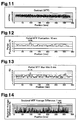
- Figs. 11 and 12 are graphs given for the rod lens array of a comparison example according to the second embodiment.
- Fig. 11 shows a distribution of the contrast (MTF) of the dot images in the image forming range and Fig. 12, a partial MTF fluctuation related to condition 1A.
- MTF contrast
- the contrast value itself does not seem to have a distinct difference from the surroundings all over the image forming range.
- the partial MTF fluctuation of the rod lens array of the comparison example is sufficiently smaller than 18% in the 10-mm sections except those near the position 95 mm but, in one 10-mm section near it, is 18.6%.
- a rod lens array 24B related to a third embodiment is manufactured in such a manner that it may satisfy condition 2A.
- Fig. 13 is a graph created for the rod lens array of the comparison example as against that of the third embodiment, showing a partial MTF max-min related to condition 2A.
- the partial MTF max-min of the rod lens array of the comparison example is 31.1%, in excess of 30%, in one narrow section (5-mm section) near the position 95 mm.
- a rod lens array 24C according to a fourth embodiment is manufactured in such a manner that it may satisfy condition 3A.
- Fig. 14 is a graph created for the rod lens array of the comparison example as against that of the fourth embodiment, showing a sectional MTF average difference related to condition 3A.
- the sectional MTF average difference of the rod lens array of the comparison example is 10.3% in one narrow section (1-mm section) near the position 275 mm and less than 10% in the other sections.
- a narrow stripe-like irregularity appeared near the position 275 mm.
- the narrow stripe-like irregularity thus appeared because the adjoining net dots had a larger difference in color density therebetween and, therefore, could not formed for representation of gradations as intended.
- a rod lens array 24D related to the fifth embodiment is manufactured in such a manner that it may satisfy condition 4A.
- an average of the dot image contrasts all over the image forming range was 44.2% (see Fig. 11) and a standard deviation thereof, 4.67%.
- a rod lens array 24E related to the sixth embodiment is manufactured in such a manner that it may satisfy condition 5A.
- an average of the dot image contrasts all over the image forming range was 44.2% (see Fig. 11) and a standard deviation thereof, 4.67%. In this case, 4.67/44.2 ⁇ 0.1 (approximately 10%).
- the rod lens array 24E satisfies condition 5A.
- the seventh embodiment uses the rod lens array 24 in which a number of small-sized gradient index rod lenses are arrayed, which rod lens array 24 is manufactured in such a manner that it may satisfy condition 6A.
- the eighth embodiment uses a gradient index rod lens array as the array 24G, which is manufactured in such a manner that it may satisfy condition 7A.
- the present embodiment uses a gradient index rod lens array 24H, which is manufactured in such a manner that it may satisfy condition 8A.
- the optical axes of the rod lenses thereof each have an angle of about 0.002 (radian) with respect to the adjoining rod lens at the relevant position.
- the rod lens array is so designed that the spacing between the light source (substance surface) and the image surface (see Fig. 3), that is, the conjugate length TC may be about 10 mm, so that the angle of the optical axis has a shift of about 20 ⁇ m on the image surface. This is roughly equal to a pitch between the light emitting dots of the 1200 dpi-specification LED array.
- rod lens array 24H of the ninth embodiment it is possible to prevent the appearance of a wide stripe-like irregularity ascribed to a shift in angle of the optical axis between the rod lenses 25. It is, therefore, possible to obtain a good picture quality free of a wide stripe-like irregularity even when many gradient index rod lenses are arranged to constitute the rod lens array 24.
- any one of the rod lens arrays 24A to 24H according to the respective second through ninth embodiments is utilized, it is possible to form a good picture-quality image free of a wide stripe-like irregularity and output it when it is printed at a high recording density of 1200 dpi.
- the optical printer 11 is capable of outputting a color image.
- a color image using an optical printer generally at least three colors, for example, yellow, magenta, cyan, and black colors, of images are superposed on each other to form the color image on the photosensitive surface of the photosensitive drum 12.
- the optical printer 11 it is necessary to arrange in the optical printer 11 a plurality of (at least three) the LED print heads 13 shown in Fig. 2 in which the LED array 23 and the rod lens array 24 are mounted.
- a stripe-like color irregularity due to a shift in color appears unless these colors of images are superposed properly.
- the stripe-like color irregularity will appear if there is a shift in position at which a dot image is formed by the rod lens arrays 24.
- the image dots are formed at a pitch of about 21 ⁇ m therebetween in the 1200 dpi-specification optical printer, so that if the formation position of the dot images is shifted by the pitch of 21 ⁇ m or more, the intended colors cannot be reproduced, thus giving rise to a stripe-like irregularity. It is necessary to reduce the image formation positional shift to about 42 ⁇ m or less in the 600 dpi-specification printer.
- a stripe-like color irregularity may sometimes appear due to a color shift.
- each color of the dot image has a shift of about 20 ⁇ m despite a small fluctuation in dot image size (dot size).
- the lens surface of the rod lens 25 is shifted by about ⁇ 0.02/TC [mm] (unit: radian) despite that it must be at 90° with respect to the lens array attachment reference surface of the rod lens array 24.
- the optical printer 11 of the tenth embodiment also comprises a plurality of (at least three) rod lens arrays 24 capable of obtaining a good picture quality free of a stripe-like irregularity.
- the plurality of rod lens arrays 24 are each assembled to the lens array attachment reference surface as adjusted to satisfy condition 9A. Accordingly, the rod lens arrays with a large fluctuation in position of the printing point are adjusted beforehand, so that the fluctuation in angle between the frame 26 of each of the rod lens arrays and the rod array attachment reference surface is reduced to about ⁇ 0.02/TC [mm] (unit: radian) or less. This enables preventing a stripe-like irregularity from appearing due to a color shift when performing process color printing using a plurality of lens arrays.
- the first inspection method comprises the following five steps:
- the first inspection method for the optical printer 11 has the following advantages.
- a judgment result can be obtained in step 5 on whether the partial MTF fluctuation in each section is roughly 18% or less, thus deciding whether a good picture quality free of a stripe-like irregularity ascribed to the rod lens array 24 can be obtained before the apparatus is assembled.
- the stripe-like irregularity ascribed to the rod lens array 24 can be checked before the assembly of the apparatus.
- the performance of the rod lens array 24 itself can be evaluated without conducting printing testing actually. Accordingly, it is possible to simplify the inspection process itself for the apparatus after being assembled and also to know a fault of the rod lens array 24 itself after the assembly of the apparatus. It is, therefore, possible to check the stripe-like irregularity ascribed to the rod lens array 24 before the apparatus is assembled, thus improving the productivity.
- the second inspection method for the optical printer 11 has changed only step 5 of steps 1 to 5 of the first inspection method.
- the second inspection method comprises the above-mentioned steps 1 to 4 and the following step 6.
- Step 6 ⁇ It is decided whether the partial MTF max-min, which is a difference between the maximum Imax and the minimum Imin of the contrasts of the dot images, in each of the sections (5-mm sections) with a predetermined width obtained by dividing the image forming range is roughly 30% or less.
- the second optical printer inspection method has the following advantages.
- step 6 a result can be obtained on whether the partial MTF max-min in each 5-mm section is roughly 30% or less, thus deciding whether a good picture quality free of a stripe-like irregularity ascribed to the rod lens array 24 can be obtained before the apparatus is assembled. It is, therefore, possible to check the stripe-like irregularity ascribed to the rod lens array 24 before the apparatus is assembled, thus improving the productivity.
- the third inspection method for the optical printer 11 has changed only step 5 of steps 1 to 5 of the first inspection method.
- the third inspection method comprises the above-mentioned steps 1 to 4 and the following step 7.
- Step 7 ⁇ It is decided whether the sectional MTF average difference, which is a difference between an average of the contrasts of the dot images in each of the sections (1-mm sections) with a predetermined width obtained by dividing the image forming range and that in the adjoining section, is roughly 10% or less.
- the third optical printer inspection method has the following advantages.
- step 7 a result can be obtained on whether the sectional MTF average difference in each 1-mm section is roughly 10% or less, thus deciding whether a good picture quality free of a stripe-like irregularity ascribed to the rod lens array 24 can be obtained before the apparatus is assembled. It is, therefore, possible to check the stripe-like irregularity ascribed to the rod lens array 24 before the apparatus is assembled, thus improving the productivity.
Landscapes
- Physics & Mathematics (AREA)
- Optics & Photonics (AREA)
- Health & Medical Sciences (AREA)
- General Health & Medical Sciences (AREA)
- Toxicology (AREA)
- General Physics & Mathematics (AREA)
- Printers Or Recording Devices Using Electromagnetic And Radiation Means (AREA)
Applications Claiming Priority (4)
| Application Number | Priority Date | Filing Date | Title |
|---|---|---|---|
| JP2001270711 | 2001-09-06 | ||
| JP2001270711A JP2003072145A (ja) | 2001-09-06 | 2001-09-06 | 光書込みヘッドおよびそれを用いた画像形成装置 |
| JP2001310226A JP2003114305A (ja) | 2001-10-05 | 2001-10-05 | レンズアレイ、それを用いた画像形成装置および画像形成装置の検査方法 |
| JP2001310226 | 2001-10-05 |
Publications (2)
| Publication Number | Publication Date |
|---|---|
| EP1291186A2 true EP1291186A2 (de) | 2003-03-12 |
| EP1291186A3 EP1291186A3 (de) | 2003-06-04 |
Family
ID=26621776
Family Applications (1)
| Application Number | Title | Priority Date | Filing Date |
|---|---|---|---|
| EP02020044A Withdrawn EP1291186A3 (de) | 2001-09-06 | 2002-09-06 | Optischer Schreibkopf, damit versehenes Bilderzeugungsgerät und Verfahren zur Inspektion dieses Gerätes |
Country Status (4)
| Country | Link |
|---|---|
| US (2) | US6891558B2 (de) |
| EP (1) | EP1291186A3 (de) |
| CN (1) | CN1326129C (de) |
| TW (1) | TW558518B (de) |
Cited By (1)
| Publication number | Priority date | Publication date | Assignee | Title |
|---|---|---|---|---|
| CN101403877B (zh) * | 2007-10-03 | 2011-05-18 | 精工爱普生株式会社 | 行头及使用了行头的图像形成装置 |
Families Citing this family (5)
| Publication number | Priority date | Publication date | Assignee | Title |
|---|---|---|---|---|
| TW558518B (en) * | 2001-09-06 | 2003-10-21 | Nippon Sheet Glass Co Ltd | Optical write-in head, image forming apparatus using the same, and method for inspecting the apparatus |
| JP2005275251A (ja) * | 2004-03-26 | 2005-10-06 | Canon Inc | 画像形成装置 |
| JP4416581B2 (ja) * | 2004-06-30 | 2010-02-17 | 株式会社沖データ | 露光装置、ledプリントヘッド及びこれを備えた画像形成装置 |
| JP4546285B2 (ja) * | 2005-02-28 | 2010-09-15 | 株式会社セイコーアイ・インフォテック | 光プリンタヘッドおよび画像形成装置 |
| WO2013146873A1 (ja) | 2012-03-30 | 2013-10-03 | 三菱レイヨン株式会社 | ロッドレンズアレイおよびそれを用いたイメージセンサヘッド |
Citations (6)
| Publication number | Priority date | Publication date | Assignee | Title |
|---|---|---|---|---|
| US5233469A (en) * | 1987-10-22 | 1993-08-03 | Canon Kabushiki Kaisha | Imaging optical system using index distribution type optical elements |
| EP0786353A1 (de) * | 1994-10-05 | 1997-07-30 | Rohm Co., Ltd. | Led-druckkopf |
| EP0926513A2 (de) * | 1997-12-24 | 1999-06-30 | Nippon Sheet Glass Co., Ltd. | Stablinsen-Matrix für optisches Abbildungssystem |
| JP2001083044A (ja) * | 1999-07-14 | 2001-03-30 | Canon Inc | レンズアレイの検査方法及び検査システム |
| EP1106366A2 (de) * | 1999-12-02 | 2001-06-13 | Canon Kabushiki Kaisha | LED-Kopf, Bilderzeugungsvorrichtung, Verfahren zum Messen der durch eine Leuchtdiodenanordnung emittierten Lichtmenge |
| JP2001205845A (ja) * | 2000-01-24 | 2001-07-31 | Hitachi Ltd | Ledプリンタヘッド、ロッドレンズアレイ及び画像形成装置 |
Family Cites Families (7)
| Publication number | Priority date | Publication date | Assignee | Title |
|---|---|---|---|---|
| SE458499B (sv) * | 1987-06-25 | 1989-04-10 | Astra Meditec Ab | Saett och anordning foer framstaellning av en tandbro |
| JP4087503B2 (ja) * | 1998-06-05 | 2008-05-21 | 三菱レイヨン株式会社 | 光伝送体、光伝送体アレイ、光伝送体アレイの使用方法及びカラーイメージセンサ |
| JP2001158128A (ja) * | 1999-12-02 | 2001-06-12 | Canon Inc | Ledプリンターヘッドとledプリンター |
| JP2001255230A (ja) | 2000-03-09 | 2001-09-21 | Nippon Sheet Glass Co Ltd | レンズアレイの結像位置ずれ評価方法 |
| JP2001264210A (ja) | 2000-03-22 | 2001-09-26 | Nippon Sheet Glass Co Ltd | レンズアレイの配列評価方法 |
| JP2001272302A (ja) | 2000-03-27 | 2001-10-05 | Nippon Sheet Glass Co Ltd | レンズアレイの光学性能評価装置 |
| TW558518B (en) * | 2001-09-06 | 2003-10-21 | Nippon Sheet Glass Co Ltd | Optical write-in head, image forming apparatus using the same, and method for inspecting the apparatus |
-
2002
- 2002-09-05 TW TW091120277A patent/TW558518B/zh not_active IP Right Cessation
- 2002-09-06 US US10/236,638 patent/US6891558B2/en not_active Expired - Lifetime
- 2002-09-06 CN CNB021320195A patent/CN1326129C/zh not_active Expired - Lifetime
- 2002-09-06 EP EP02020044A patent/EP1291186A3/de not_active Withdrawn
-
2004
- 2004-04-19 US US10/828,393 patent/US7071963B2/en not_active Expired - Fee Related
Patent Citations (6)
| Publication number | Priority date | Publication date | Assignee | Title |
|---|---|---|---|---|
| US5233469A (en) * | 1987-10-22 | 1993-08-03 | Canon Kabushiki Kaisha | Imaging optical system using index distribution type optical elements |
| EP0786353A1 (de) * | 1994-10-05 | 1997-07-30 | Rohm Co., Ltd. | Led-druckkopf |
| EP0926513A2 (de) * | 1997-12-24 | 1999-06-30 | Nippon Sheet Glass Co., Ltd. | Stablinsen-Matrix für optisches Abbildungssystem |
| JP2001083044A (ja) * | 1999-07-14 | 2001-03-30 | Canon Inc | レンズアレイの検査方法及び検査システム |
| EP1106366A2 (de) * | 1999-12-02 | 2001-06-13 | Canon Kabushiki Kaisha | LED-Kopf, Bilderzeugungsvorrichtung, Verfahren zum Messen der durch eine Leuchtdiodenanordnung emittierten Lichtmenge |
| JP2001205845A (ja) * | 2000-01-24 | 2001-07-31 | Hitachi Ltd | Ledプリンタヘッド、ロッドレンズアレイ及び画像形成装置 |
Non-Patent Citations (2)
| Title |
|---|
| PATENT ABSTRACTS OF JAPAN vol. 2000, no. 20, 10 July 2001 (2001-07-10) & JP 2001 083044 A (CANON INC), 30 March 2001 (2001-03-30) * |
| PATENT ABSTRACTS OF JAPAN vol. 2000, no. 24, 11 May 2001 (2001-05-11) & JP 2001 205845 A (HITACHI LTD), 31 July 2001 (2001-07-31) * |
Cited By (1)
| Publication number | Priority date | Publication date | Assignee | Title |
|---|---|---|---|---|
| CN101403877B (zh) * | 2007-10-03 | 2011-05-18 | 精工爱普生株式会社 | 行头及使用了行头的图像形成装置 |
Also Published As
| Publication number | Publication date |
|---|---|
| EP1291186A3 (de) | 2003-06-04 |
| CN1407548A (zh) | 2003-04-02 |
| US20040196355A1 (en) | 2004-10-07 |
| TW558518B (en) | 2003-10-21 |
| US6891558B2 (en) | 2005-05-10 |
| US7071963B2 (en) | 2006-07-04 |
| US20030043255A1 (en) | 2003-03-06 |
| CN1326129C (zh) | 2007-07-11 |
Similar Documents
| Publication | Publication Date | Title |
|---|---|---|
| US7898738B2 (en) | Lens array, manufacturing method thereof, LED head having lens array, exposure device having LED head, image forming apparatus having exposure device, and reading apparatus | |
| US7933070B2 (en) | Lens array, light emitting diode head, exposure device, image forming apparatus, and image reading apparatus | |
| JP4490494B2 (ja) | レンズアレイ製造方法、レンズアレイ、ledヘッド、露光装置、画像形成装置及び読取装置 | |
| US7417659B2 (en) | Exposure device, LED print head, and image forming apparatus having the exposure device and the LED print head | |
| JP5584262B2 (ja) | レンズユニット、ledヘッド、露光装置、画像形成装置および読取装置 | |
| JP4714765B2 (ja) | レンズアレイ、ledプリントヘッド、露光装置、画像形成装置及び読取装置 | |
| JP2010164658A (ja) | レンズアレイ、レンズユニット、ledヘッド、露光装置、画像形成装置および読取装置 | |
| US20100202059A1 (en) | Lens array, light emitting diode head, exposure device, image forming apparatus, and reading apparatus | |
| US20130135694A1 (en) | Lens array, lens unit, led head, exposure device, image formation apparatus, and image reading apparatus | |
| US8000015B2 (en) | Lens unit, LED head, exposing unit, image forming apparatus, and scanning apparatus | |
| US8797651B2 (en) | Lens array, lens unit, LED head, exposure unit, image formation apparatus, reading apparatus, mold for molding lens array, and method for manufacturing lens array | |
| US20090322847A1 (en) | Exposure device, LED head, image forming apparatus, and reading apparatus | |
| US20090091611A1 (en) | Line Head and Image Forming Apparatus Using the Same | |
| US6891558B2 (en) | Optical write-in head, image forming apparatus using the same, and method for inspecting the apparatus | |
| US7145590B2 (en) | Apparatus with offset light source for forming images on photosensitive surface | |
| US7764382B2 (en) | Illuminator for specular measurements | |
| JP2010164717A (ja) | レンズアレイ、レンズユニット、ledヘッド、露光装置、画像形成装置および読取装置 | |
| JP2007147438A (ja) | レンズアレイの評価方法、評価装置、レンズアレイ、および画像形成装置 | |
| JP3363876B2 (ja) | レンズアレイの検査方法及び検査システム | |
| US20010013888A1 (en) | LED head, image forming apparatus, and method of measuring amount of light from LED array | |
| JP2003114305A (ja) | レンズアレイ、それを用いた画像形成装置および画像形成装置の検査方法 | |
| US20060197011A1 (en) | Image forming apparatus | |
| JP2001322309A (ja) | 画像形成装置 | |
| JP2003114305A5 (de) | ||
| JP4591135B2 (ja) | 露光装置および画像形成装置 |
Legal Events
| Date | Code | Title | Description |
|---|---|---|---|
| PUAI | Public reference made under article 153(3) epc to a published international application that has entered the european phase |
Free format text: ORIGINAL CODE: 0009012 |
|
| AK | Designated contracting states |
Kind code of ref document: A2 Designated state(s): AT BE BG CH CY CZ DE DK EE ES FI FR GB GR IE IT LI LU MC NL PT SE SK TR Designated state(s): AT BE BG CH CY CZ DE DK EE ES FI FR GB GR IE IT LI LU MC NL PT SE SK TR |
|
| AX | Request for extension of the european patent |
Extension state: AL LT LV MK RO SI |
|
| PUAL | Search report despatched |
Free format text: ORIGINAL CODE: 0009013 |
|
| AK | Designated contracting states |
Designated state(s): AT BE BG CH CY CZ DE DK EE ES FI FR GB GR IE IT LI LU MC NL PT SE SK TR |
|
| AX | Request for extension of the european patent |
Extension state: AL LT LV MK RO SI |
|
| 17P | Request for examination filed |
Effective date: 20031024 |
|
| AKX | Designation fees paid |
Designated state(s): AT BE BG CH CY CZ DE DK EE ES FI FR GB GR IE IT LI LU MC NL PT SE SK TR |
|
| STAA | Information on the status of an ep patent application or granted ep patent |
Free format text: STATUS: THE APPLICATION IS DEEMED TO BE WITHDRAWN |
|
| 18D | Application deemed to be withdrawn |
Effective date: 20050401 |