EP1289008A2 - Halbleitervorrichtung und deren Herstellungsverfahren - Google Patents
Halbleitervorrichtung und deren Herstellungsverfahren Download PDFInfo
- Publication number
- EP1289008A2 EP1289008A2 EP02007245A EP02007245A EP1289008A2 EP 1289008 A2 EP1289008 A2 EP 1289008A2 EP 02007245 A EP02007245 A EP 02007245A EP 02007245 A EP02007245 A EP 02007245A EP 1289008 A2 EP1289008 A2 EP 1289008A2
- Authority
- EP
- European Patent Office
- Prior art keywords
- layer
- wiring
- via plug
- forms
- film
- Prior art date
- Legal status (The legal status is an assumption and is not a legal conclusion. Google has not performed a legal analysis and makes no representation as to the accuracy of the status listed.)
- Withdrawn
Links
Images



Classifications
-
- H—ELECTRICITY
- H10—SEMICONDUCTOR DEVICES; ELECTRIC SOLID-STATE DEVICES NOT OTHERWISE PROVIDED FOR
- H10P—GENERIC PROCESSES OR APPARATUS FOR THE MANUFACTURE OR TREATMENT OF DEVICES COVERED BY CLASS H10
- H10P14/00—Formation of materials, e.g. in the shape of layers or pillars
- H10P14/40—Formation of materials, e.g. in the shape of layers or pillars of conductive or resistive materials
-
- H—ELECTRICITY
- H10—SEMICONDUCTOR DEVICES; ELECTRIC SOLID-STATE DEVICES NOT OTHERWISE PROVIDED FOR
- H10W—GENERIC PACKAGES, INTERCONNECTIONS, CONNECTORS OR OTHER CONSTRUCTIONAL DETAILS OF DEVICES COVERED BY CLASS H10
- H10W20/00—Interconnections in chips, wafers or substrates
- H10W20/01—Manufacture or treatment
- H10W20/031—Manufacture or treatment of conductive parts of the interconnections
- H10W20/032—Manufacture or treatment of conductive parts of the interconnections of conductive barrier, adhesion or liner layers
- H10W20/033—Manufacture or treatment of conductive parts of the interconnections of conductive barrier, adhesion or liner layers in openings in dielectrics
-
- H—ELECTRICITY
- H10—SEMICONDUCTOR DEVICES; ELECTRIC SOLID-STATE DEVICES NOT OTHERWISE PROVIDED FOR
- H10W—GENERIC PACKAGES, INTERCONNECTIONS, CONNECTORS OR OTHER CONSTRUCTIONAL DETAILS OF DEVICES COVERED BY CLASS H10
- H10W20/00—Interconnections in chips, wafers or substrates
- H10W20/01—Manufacture or treatment
- H10W20/031—Manufacture or treatment of conductive parts of the interconnections
- H10W20/032—Manufacture or treatment of conductive parts of the interconnections of conductive barrier, adhesion or liner layers
- H10W20/033—Manufacture or treatment of conductive parts of the interconnections of conductive barrier, adhesion or liner layers in openings in dielectrics
- H10W20/036—Manufacture or treatment of conductive parts of the interconnections of conductive barrier, adhesion or liner layers in openings in dielectrics the barrier, adhesion or liner layers being within a main fill metal
-
- H—ELECTRICITY
- H10—SEMICONDUCTOR DEVICES; ELECTRIC SOLID-STATE DEVICES NOT OTHERWISE PROVIDED FOR
- H10W—GENERIC PACKAGES, INTERCONNECTIONS, CONNECTORS OR OTHER CONSTRUCTIONAL DETAILS OF DEVICES COVERED BY CLASS H10
- H10W20/00—Interconnections in chips, wafers or substrates
- H10W20/01—Manufacture or treatment
- H10W20/031—Manufacture or treatment of conductive parts of the interconnections
- H10W20/032—Manufacture or treatment of conductive parts of the interconnections of conductive barrier, adhesion or liner layers
- H10W20/033—Manufacture or treatment of conductive parts of the interconnections of conductive barrier, adhesion or liner layers in openings in dielectrics
- H10W20/037—Manufacture or treatment of conductive parts of the interconnections of conductive barrier, adhesion or liner layers in openings in dielectrics the barrier, adhesion or liner layers being on top of a main fill metal
-
- H—ELECTRICITY
- H10—SEMICONDUCTOR DEVICES; ELECTRIC SOLID-STATE DEVICES NOT OTHERWISE PROVIDED FOR
- H10W—GENERIC PACKAGES, INTERCONNECTIONS, CONNECTORS OR OTHER CONSTRUCTIONAL DETAILS OF DEVICES COVERED BY CLASS H10
- H10W20/00—Interconnections in chips, wafers or substrates
- H10W20/01—Manufacture or treatment
- H10W20/031—Manufacture or treatment of conductive parts of the interconnections
- H10W20/032—Manufacture or treatment of conductive parts of the interconnections of conductive barrier, adhesion or liner layers
- H10W20/038—Manufacture or treatment of conductive parts of the interconnections of conductive barrier, adhesion or liner layers covering conductive structures
-
- H—ELECTRICITY
- H10—SEMICONDUCTOR DEVICES; ELECTRIC SOLID-STATE DEVICES NOT OTHERWISE PROVIDED FOR
- H10W—GENERIC PACKAGES, INTERCONNECTIONS, CONNECTORS OR OTHER CONSTRUCTIONAL DETAILS OF DEVICES COVERED BY CLASS H10
- H10W20/00—Interconnections in chips, wafers or substrates
- H10W20/01—Manufacture or treatment
- H10W20/031—Manufacture or treatment of conductive parts of the interconnections
- H10W20/056—Manufacture or treatment of conductive parts of the interconnections by filling conductive material into holes, grooves or trenches
-
- H—ELECTRICITY
- H10—SEMICONDUCTOR DEVICES; ELECTRIC SOLID-STATE DEVICES NOT OTHERWISE PROVIDED FOR
- H10W—GENERIC PACKAGES, INTERCONNECTIONS, CONNECTORS OR OTHER CONSTRUCTIONAL DETAILS OF DEVICES COVERED BY CLASS H10
- H10W20/00—Interconnections in chips, wafers or substrates
- H10W20/01—Manufacture or treatment
- H10W20/031—Manufacture or treatment of conductive parts of the interconnections
- H10W20/056—Manufacture or treatment of conductive parts of the interconnections by filling conductive material into holes, grooves or trenches
- H10W20/057—Manufacture or treatment of conductive parts of the interconnections by filling conductive material into holes, grooves or trenches by selectively depositing, e.g. by using selective CVD or plating
-
- H—ELECTRICITY
- H10—SEMICONDUCTOR DEVICES; ELECTRIC SOLID-STATE DEVICES NOT OTHERWISE PROVIDED FOR
- H10W—GENERIC PACKAGES, INTERCONNECTIONS, CONNECTORS OR OTHER CONSTRUCTIONAL DETAILS OF DEVICES COVERED BY CLASS H10
- H10W20/00—Interconnections in chips, wafers or substrates
- H10W20/40—Interconnections external to wafers or substrates, e.g. back-end-of-line [BEOL] metallisations or vias connecting to gate electrodes
- H10W20/41—Interconnections external to wafers or substrates, e.g. back-end-of-line [BEOL] metallisations or vias connecting to gate electrodes characterised by their conductive parts
- H10W20/42—Vias, e.g. via plugs
-
- H—ELECTRICITY
- H10—SEMICONDUCTOR DEVICES; ELECTRIC SOLID-STATE DEVICES NOT OTHERWISE PROVIDED FOR
- H10W—GENERIC PACKAGES, INTERCONNECTIONS, CONNECTORS OR OTHER CONSTRUCTIONAL DETAILS OF DEVICES COVERED BY CLASS H10
- H10W20/00—Interconnections in chips, wafers or substrates
- H10W20/40—Interconnections external to wafers or substrates, e.g. back-end-of-line [BEOL] metallisations or vias connecting to gate electrodes
- H10W20/41—Interconnections external to wafers or substrates, e.g. back-end-of-line [BEOL] metallisations or vias connecting to gate electrodes characterised by their conductive parts
- H10W20/425—Barrier, adhesion or liner layers
-
- H—ELECTRICITY
- H10—SEMICONDUCTOR DEVICES; ELECTRIC SOLID-STATE DEVICES NOT OTHERWISE PROVIDED FOR
- H10W—GENERIC PACKAGES, INTERCONNECTIONS, CONNECTORS OR OTHER CONSTRUCTIONAL DETAILS OF DEVICES COVERED BY CLASS H10
- H10W20/00—Interconnections in chips, wafers or substrates
- H10W20/40—Interconnections external to wafers or substrates, e.g. back-end-of-line [BEOL] metallisations or vias connecting to gate electrodes
- H10W20/41—Interconnections external to wafers or substrates, e.g. back-end-of-line [BEOL] metallisations or vias connecting to gate electrodes characterised by their conductive parts
- H10W20/44—Conductive materials thereof
- H10W20/4403—Conductive materials thereof based on metals, e.g. alloys, metal silicides
- H10W20/4437—Conductive materials thereof based on metals, e.g. alloys, metal silicides the principal metal being a transition metal
- H10W20/4441—Conductive materials thereof based on metals, e.g. alloys, metal silicides the principal metal being a transition metal the principal metal being a refractory metal
Definitions
- the present invention generally relates to a semiconductor device and a manufacturing method thereof, and particularly relates to the semiconductor device that has multilayer interconnection structure, and the manufacturing method thereof.
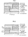
- Fig. 1 is a figure explaining wiring structure of a conventional semiconductor device.
- a silicon dioxide (SiO 2 ) film 11 is formed as an inter-layer film in a device (not shown) formed on a semiconductor substrate 10.
- Cu wiring 15 is formed as lower layer wiring through a barrier metal layer 13 that is made of a material such as tantalum nitride and tantalum.
- an SiO 2 film 17 is formed on the SiO2 film 11, as an inter-layer film, wrapping the Cu wiring 15.
- a via plug 21 is formed such that the SiO 2 film 17 is penetrated and the Cu wiring 15 is touched through a barrier metal layer 19 that is made of a material such as tantalum nitride and tantalum.
- Cu wiring 23 serving as upper wiring is formed contiguously with the via plug 21 that touches the Cu wiring 15 through the barrier metal layer 19 that is made of a material such as tantalum nitride and tantalum. Further, on the SiO 2 film 17, an SiO 2 film 25 is formed, contacting with the barrier metal layer 19.
- the copper atom in the via plug 21 tends to move toward the direction of the Cu wiring 23, like electron flow, according to an electro migration phenomenon. Consequently, a void occurs on the side of the Cu wiring 15 of the via plug 21, due to the copper atom in the via plug 21 moving.
- Cu wiring that has a lower electric resistance than aluminum wiring.
- dual damascene processing is being established. All elements of a lamination, wiring - via plug - wiring, are made of Cu. Since the atomic weight of Cu is larger than aluminum, Cu is more resistive against electro migration. However, local current concentration still arises to a via plug in the Cu wiring laminated structure that is miniaturized, causing a poor wiring by a void generated as explained above.
- a general object of the present invention is to provide a semiconductor device and a manufacturing method thereof that substantially obviate one or more of the problems caused by the limitations and disadvantages of the related art.
- the invention provides the semiconductor device in which electro migration is suppressed, while maintaining a high-speed operation, paying attention to the structure of the via plug, and its manufacturing method.
- the semiconductor device of the present invention includes a first wiring and a second wiring that are prepared on an upper surface and under a lower surface, respectively, of an inter-layer insulation film, and a via plug that connects the first wiring and the second wiring.
- the via plug is configured to include at least one layer of a high melting-point metal, thickness of which is a part of the thickness of the via plug, and the metal that forms this layer has a melting point that is higher than the melting point of the metal that forms the first wiring and the second wiring.
- the via plug it is desirable to have one layer of high melting-point metal, and, it is desirable that the laminating is carried out such that the high melting-point metal layer touches the first wiring and the second wiring through a barrier metal layer.
- the first wiring, the second wiring, and the via plug are formed by copper or a copper alloy, and the high melting-point metal layer is formed by a tungsten. Further, it is desirable that the high melting-point metal layer is formed in a thickness that ranges between 10 nm and 100 nm.
- the high melting-point metal layer can be formed on a surface of the metal exposed in the via plug by a chemical vapor depositing method, for example, choosing suitable deposition conditions, and suppressing deposition on the inter-layer insulation film surface, in a self-aligning forming without using a mask process.
- the semiconductor device of the present invention has multilayer interconnection structure, and embodiments of the present invention employ Cu wiring structure that is attracting attention as the wiring structure that contributes to a fast operation.
- new structure of a via plug which suppresses the electro migration of Cu in Cu wiring structure is illustrated.
- selection criterion of a metal that forms a part of the thickness of the via plug, requirements of the metal layer from a viewpoint of the electro migration of Cu, and the like will be described.
- a middle layer of a high melting-point metal such as tungsten (W)
- W tungsten
- the middle layer of the high melting-point metal can be formed in a self-alignment manner, avoiding an increase in the number of mask processes.
- Fig. 2 is a figure explaining wiring structure of the semiconductor device of the embodiments of the present invention.
- the semiconductor device of the embodiment has multilayer interconnection structure that employs Cu wiring 35 and Cu wiring 43.
- a Cu layer 42 formed contiguously with the Cu wiring 43, and a W layer 47 as a high melting-point metal layer are included.
- the metal material adopted as this high melting-point metal layer is chosen with reference to the melting point and the specific resistance of Cu that forms the Cu wiring 35, the Cu wiring 43, and the Cu layer 42, and is formed in predetermined thickness.
- a silicon dioxide (SiO 2 ) film 31 as an inter-layer film to wrap a device (not shown) formed on this substrate.
- the SiO 2 film 31 is formed in about 400 nm thickness.
- a barrier metal layer 33 is formed on the SiO 2 film 31.
- the barrier metal layer 33 is formed in order that the atom of Cu used as wiring material is prevented from being spread in the SiO 2 film 31 in a wiring process etc.
- the barrier metal layer 33 is formed in about 20 nm thickness in the present embodiment.
- the Cu wiring 35 serving as lower layer wiring is formed on the barrier metal layer 33.
- the Cu wiring 35 is formed in about 300 nm thickness.
- the SiO 2 film 37 is formed in about 400 nm thickness in the present embodiment.
- the via plug 41 penetrates the SiO 2 film 37, and connects the Cu wiring 35 and the Cu wiring 43.
- the via plug 41 in the present embodiment includes a W layer 47 as the high melting-point metal layer, and a Cu layer 42 formed contiguously with the Cu wiring 43.
- a barrier metal layer 39 is formed on the SiO 2 film 37.
- the barrier metal layer 39 has two roles in the present embodiment. A first role is preventing the atom of Cu used as wiring material from being spread in the SiO 2 film 37 and the SiO 2 film 45 during wiring process etc. A second role is forming a double layer with the W layer 47 in order to prevent Cu from spreading (double Cu spread prevention layer), and preventing Cu atom from spreading by electro migration.
- the barrier metal layer 39 is formed in about 20 nm thickness in the present embodiment.
- the Cu wiring 43 serving as upper wiring is continuously formed with the Cu layer 42.
- the Cu wiring 43 is formed in about 300 nm thickness in the present embodiment.
- an SiO 2 film 45 as inter-layer film is formed so that the Cu wiring 43 may be surrounded.
- SiO 2 film 45 is formed in about 400 nm thickness in the present embodiment.
- the W layer 47 is prepared in a lower part of the via plug 41, and an undersurface of the W layer 47 is directly in contact with the Cu wiring 35. On the other hand, an upper surface of the W layer 47 is in contact with the Cu layer 42 through the barrier metal layer 39. Therefore, in the present embodiment, the barrier metal layer 39 is formed between the W layer 47 and the Cu layer 42 that constitute the via plug 41.
- Thickness of the via plug 41 prepared by penetrating the SiO 2 film 37 is about 400 nm, of which about 50 nm is occupied by the W layer 47.
- the W layer 47 is formed very thinly so that the low resistance of the Cu wiring is not spoiled.
- the semiconductor device of the present embodiment has the wiring structure that includes the Cu wiring 35 and the Cu wiring 43, and the via plug 41 that connects the Cu wiring 35 and the Cu wiring 43 that are formed on the upper and the lower surfaces of the SiO 2 film 37, respectively.
- the via plug 41 includes a W layer 47 as a metal layer that has a melting point higher than Cu that is used as wiring metal.
- a first viewpoint is selecting a material as the high melting-point metal layer as a means for suppressing the migration of Cu (refer to Fig. 3).
- a second viewpoint is thickness (refer to Fig. 4) of the metal layer, which affects operation speed of the semiconductor device.
- the via plug 41 has the tungsten (W) layer 47 as a high melting-point metal layer in addition to the Cu layer 42 so that the Cu wiring 35 is connected directly.
- Tungsten (W) has a melting point higher than copper (Cu) that forms the Cu wiring 35, the Cu wiring 43 and the Cu layer 42.
- Fig. 3 is a list of metal materials applicable to the semiconductor device of the present embodiment as the high melting-point metal layer.
- a first requirement of the metal layer formed in a part of the via plug 41 in the Cu wiring is to suppress an electron transfer (movement of a copper atom) within the via plug 41 where electric current concentrates. Accordingly, metal that has a capability to suppress the electron transfer (movement of a copper atom) is searched. Specifically, metal material with a high melting point (or an atomic number is large) compared with Cu that is the wiring metal is chosen. This is based on "the higher the melting point of metal is, the harder the metal atom moves". In addition, metal to be chosen must not react with Cu that is wiring metal, otherwise the metal forms a high resistance layer.
- Fig.3 shows melting points and specific resistances of metal materials, such as gold (Au), silver (Ag), and cobalt (Co).
- metal materials such as gold (Au), silver (Ag), and cobalt (Co).
- tungsten (W) that has a melting point of 3387 degrees C, i.e., more than 3 times as high as copper (Cu) (1084.5 degrees C) is chosen.
- wiring process by the self-alignment by CVD becomes possible by using tungsten (W) .
- the barrier metal layer 39 prepared between the Cu layer 42 and the W layer 47 suppresses spreading of Cu by the electro migration, like the 47 W layer. Electro migration resistance is reinforced in this manner by a double layer of the barrier metal layer 39 and the W layer 47.
- the W layer has very thin thickness, being formed in a small part of the thickness of the via plug 41. This is because the specific resistance of W (about 4.9 ⁇ -cm) is greater than the specific resistance of Cu (about 1.56 ⁇ -cm). By making a total resistance of the via plug 41 as low as possible, an amount of delay of the whole Cu wiring can be reduced, and a high-speed operation is attained.
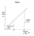
- Fig. 4 is a figure that explains about thickness of the W layer 47 in the semiconductor device of the present embodiment. This figure illustrates a basic concept of how an amount of delay in the whole Cu wiring increases with thickening of the W layer 47.
- Thickness of the W layer 47 is determined by a degree of Cu spreading at a certain temperature, when an electric field is impressed between the Cu wiring 35 and the Cu wiring 43 through the via plug 41.
- the thickness of the W layer 47 prepared in order to suppress spread of Cu to some extent can be formed very thinly (about 50 nm) compared with thickness of the via plug 41 (about 400 nm) that is the same as the SiO 2 film 37.
- the thickness of the W layer of 47 is set between 10 nm and 100 nm as shown in Fig. 4. If the thickness is set at 10 nm or less, spread of Cu becomes large, and if the thickness is set at 100 nm or more, electric resistance of the W layer 47 becomes large, causing the amount of delay of the whole Cu wiring including the via plug 41 to become large. Thus, the high-speed operation attained by the Cu wiring that has low resistance is kept available by choosing the thickness of the W layer 47 appropriately.
- Fig. 5 explains restrictions concerning the thickness of the W layer 47.
- the barrier metal layer 39 works not only during wiring process and the like, but also during operation, contributing to suppress the Cu spreading. According to this structure, the thickness of the W layer 47 can further be reduced, by selecting a material, thickness, and the like of the barrier metal layer 39.
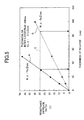
- Fig. 5 is a figure explaining thickness range of the W layer 47 of the semiconductor device of the embodiment.
- the thickness of the W layer 47 will be explained based on estimation of wiring resistance calculated.
- R1 is resistance of Cu and R2 is resistance of W.
- ⁇ 1 is the specific resistance (2.1 ⁇ -cm) of Cu
- ⁇ 2 is the specific resistance (10 ⁇ -cm) of W (here, the specific resistance of CVD-W is used).
- L1 is the thickness of Cu (the Cu layer 42) that forms a part of the via plug 41
- L2 is the thickness of W (the W layer 47) that forms another part of the via plug 41.
- S is equivalent to ⁇ d 2 /4, where D is a diameter of the via plug.
- the range of the thickness of the W layer specified in the present embodiment is prescribed by the minimum based on the solid straight line A, and the maximum based by the dashed straight line B. Specifically, the range is prescribed by restrictions from a presently available thin film growing process of the W layer 47 based on the solid straight line A, and from the outside about the device design including elements by a prospective improvement in technology as indicated by the dashed straight line B. These points will be explained in detail in the following.
- the resistance increase ratio permissible per via plug is set at 30% (level "C” in Fig.5) in the present embodiment.
- the 30% level is permissible conditions required from the outside, such as circuit design.
- the specific resistance in the bulk value of W is taken into consideration, up to 90 nm (not shown) is permissible. If the specific resistance in the present W-CVD is taken into consideration, up to about 30 nm is permissible, based on the solid straight line A. Furthermore, it is expected that the specific resistance of W-CVD gets lower in the future such that up to about 100 nm will be permissible based on the dashed straight line B.
- the range of about 10 to about 100 nm is the optimum thickness range of the W layer 47, at which both the electro migration resistance of Cu and the wiring resistance are satisfactory.
- Fig. 6 is a manufacturing process flowchart explaining the manufacturing method of the semiconductor device of the embodiment.
- the process flow by dual damascene of a two-layer wiring that has lower layer wiring and upper wiring is explained using Fig.6(A) through Fig.6(D).
- the SiO 2 film 31 is first formed as inter-layer film on the Si substrate 30.
- the SiO 2 film 31 is formed in about 400 nm thickness by a plasma-CVD method.
- the silicon-nitride (SiN) film 48 as an etching stopper is formed.
- the silicon-nitride (SiN) film 48 is formed in about 30 nm thickness by the CVD or a sputtering method.
- a trench that is an area in which the Cu wiring 35 is formed is opened by width of about 0.2 micrometers by a photolithography process and an etching process.
- photoresist on a surface of the SiN film 48 is removed, and the SiN film 48 including a surface of the trench is washed by resist removal process and washing process, respectively.
- the barrier metal layer 33 and a Cu seed layer are formed by PVD on the surface of the trench.
- the barrier metal layer 33 is formed at about 20 nm thickness, using TaN as the material.
- the Cu seed layer is formed in about 100 nm thickness by CVD or sputtering.
- a plating film of Cu is formed by a plating process, and the trench is padded.
- the plating film of Cu is formed in about 300 nm thickness by electrolysis plating.
- a Cu layer and a barrier metal layer (not shown) that are left behind on the first wiring layer are removed by a CMP process.
- the SiO 2 film 37 is formed as an inter-layer insulation film.
- This SiO 2 film 37 corresponds to a layer (not shown) in which the via plug 41 is formed.
- the thickness of the SiO 2 film 37 is made about 400 nm by the plasma-CVD method.
- the SiN film 49 as an etching stopper is formed on the SiO 2 film 37.
- the SiN film 49 is formed in about 30 nm thickness by CVD or the sputtering method.
- the SiO 2 film 45 as inter-layer film is formed on the SiN film 49.
- the SiO 2 film 45 corresponds to the second wiring layer in which the Cu wiring 43 is formed.
- the SiO 2 film 45 is formed in about 400 nm thickness by the plasma-CVD method.
- the via hole 38 of about 0.2 micrometer width is formed such that the Cu wiring 35 is exposed through the SiO 2 films 37 and 45 and the SiN film 49 by a photolithography/etching process.
- the via hole 38 is an upward opening in which the via plug 41 is formed.
- photoresist on the SiO 2 film 45 is removed, and a surface of the SiO 2 film 45 including a surface of the via hole 38 is washed by a resist removal/washing process.
- the W layer 47 is formed by CVD, reference being made to Fig. 6(B).
- the W layer 47 is formed in 50 nm thickness, using tungsten hexacarbonyl W(CO)6 as the material.
- Fig.7 shows a vapor pressure curve of W(CO)6 used in the present embodiment. Since the vapor pressure of the W(CO)6 is comparatively high, the W(CO)6 can be easily supplied at a material temperature being normal temperature, and growth of W on a substrate (Cu in this case) is rate-determined by supply.
- the growth under low gas pressure is desirable. Specifically, the growth was carried out at the substrate temperature of 300 degrees C, gas amount-of-supply 100 sccm, and pressure 100 pa. The growth rate of W in this case was 15 nm/min. W grows selectively in an area with many active spots. Therefore, W does not grow on the SiO 2 films 37 and 45, in this case. In addition, the selection ratio of Cu and SiO 2 at the time of depositing W(CO) 6 is infinite.
- W(CO)6 is supplied from above the SiO 2 film 45 by the CVD deposition process, deposition of W on the SiO 2 film 37 is suppressed by setting deposition conditions in a desirable range, and W(CO)6 is deposited selectively on the Cu wiring 35 exposed in the via hole 38, forming the W layer 47.
- the barrier metal layer 39 and the Cu seed layer 44 are formed here.
- the barrier metal is formed in about 20 nm thickness by PVD, using a tantalum nitride (TaN) as a metal that forms the barrier metal layer 39.
- the Cu seed layer 44 is formed in about 100 nm thickness.
- the plating film of Cu is formed by a plating process.
- This plating film is embedded to the via hole 38 and the opening area of an upper part of the via plug 38, and it is formed in about 300 nm thickness by electrolysis plating.
- the Cu seed layer, the barrier metal layer, and the Cu plating film (not shown), etc. that are formed above the second wiring layer (SiO 2 film 45) are removed by CMP process, and the process of the second wiring layer is finished. Thereby, the via plug 41 (Cu layer 42) and the Cu wiring 43 are formed.
- the manufacturing method of the semiconductor device of the embodiment is realized by the following processes. First, the Cu wiring 35 is formed on the SiO 2 film 31 prepared on the silicon substrate 10. Next, a wrap SiO 2 film 37 is formed for the Cu wiring 35, and the via hole 38 that penetrates this SiO 2 film 37 and exposes the Cu wiring 35 is formed.
- the W layer 47 using tungsten with a melting point higher than Cu, is then formed on the Cu wiring 35 exposed in the via hole 38. Finally, the Cu layer 42 and the Cu wiring 43 are formed through barrier metal layer 39 and others.
- tungsten (W) can be deposited selectively on the Cu wiring 35 in a CVD process by using W as a metal that forms the high melting-point metal layer.
- W(CO)6 can be used at a comparatively low temperature, and a highly thin layer can be formed by self-alignment.
- the W layer 47 only one layer (the W layer 47) of high melting-point metal is prepared in the lower part of the via plug 41 in order to maintain a high-speed operation and to suppress the migration of Cu.
- the undersurface of the W layer 47 touches the Cu wiring 35, and the upper surface of the W layer 47 touches the barrier metal layer 39, thereby the double contiguous Cu spreading prevention layer is formed.
- the present invention is not limited to this embodiment.
- a single layer of tungsten (W) may be provided in an upper part of the via plug 41, as described in the following.
- Fig. 8 is a figure explaining the wiring structure of the semiconductor device of another embodiment of the present invention.
- the same reference numbers are is given to the same units as Fig. 2, and descriptions thereof are omitted.
- a single layer of tungsten, W layer 47 is prepared in the upper part of the via plug 41.
- the W layer 47 touches the Cu layer 42 on the undersurface, and is in contact with the Cu wiring 43 through the barrier metal layer 39 on the upper surface.
- the wiring structure shown in Fig. 8 includes a double contiguous Cu spread prevention layer on the Cu wiring 43 side, while the double contiguous Cu spread prevention layer in Fig.2 is provided on the Cu wiring 35 side. Furthermore, with the wiring structure of Fig.8, the barrier metal layer 39 is provided at the lower part of the via plug 41, touching with the Cu wiring 35.
- the W layer 47 is prepared in the lower part of the via plug 41 with the wiring structure shown in Fig. 2, and is prepared in the upper part of the via plug 41 with the wiring structure shown in Fig. 8.
- the W layer 47 may also be provided in a middle part of the via plug 41 such that the Cu wiring 35 and the Cu wiring 43 are not directly touched through the barrier metal layer.
- the process of forming the via plug 41 shown in Fig. 8 is explained corresponding to explanations of Fig. 6(B) and Fig.6(C) 6.
- the two-layer wiring that has the lower layer wiring and the upper wiring is formed by a single damascene method.
- the barrier metal layer 39 and the Cu seed layer 44 are formed by PVD in the structure of Fig. 6 (A).
- the barrier metal layer 39 is not formed in the opening of the via hole 38 at this stage.
- a Cu plating film is embedded, and the Cu layer 42 is formed.
- the opening of the via hole 38 is made higher than the upper surface of the Cu layer 42 by the thickness of the W layer 47, forming a convex.
- tungsten (W) is deposited on the convex shaped opening portion by CVD, such that the W layer 47 is formed, and the via plug 41 is formed.
- the barrier metal layer 39 is formed on the upper surface of the via plug 41, and the wiring process of the second wiring layer (Cu wiring 43) is performed.
- W layer 47 only one layer of high melting-point metal layers (W layer 47) is prepared in the via plug 41.
- the present invention is not limited to these embodiments, but rather two or more W layers 47 may be provided in the via plug 41, if a demand for a high-speed operation is somewhat relaxed. Hereafter, this point is explained in detail.
- Fig. 9 is a figure explaining the wiring structure of the semiconductor device of another embodiment of the present invention.
- the same reference numbers are given to the same units in Fig. 2, and explanations thereof are omitted.
- Fig. 9 two W layers 47 are prepared in the via plug 41. Each of the W layers 47 is in contact with the Cu layers 42 on the upper surface and undersurface.
- the laminating is structured as (Cu wiring 35-) barrier metal layer 39 - Cu layer 42 - W layer 47 - Cu layer 42 - W layer 47 - Cu layer 42 - barrier metal layer 39 (-Cu wiring 43).
- Each of the W layers 47 is not in contact with the barrier metal layer 39 prepared in the upper surface and the undersurface of the via plug 41, as illustrated in Fig. 9.
- wiring structure where one or both of the W layers 47 touch the barrier metal layer 39 of the upper part and the lower part is possible.
- the barrier metal layer 39 and the Cu seed layer 44 are formed by PVD to the structure of Fig. 6(A).
- the barrier metal layer 39 is not formed in the opening of the via hole 38 in this stage.
- the process that embeds Cu plating film and forms the Cu layer 42, and the process that deposits the W layer 47 by CVD are repeated alternately, and the via plug 41 is formed.
- the barrier metal layer 39 is formed on the upper surface of the via plug 41, and the wiring process of the second wiring layer (Cu wiring 43) is performed.
- the semiconductor device of the present invention includes the via plug 41 that includes at least one high melting-point metal layer (W layer 47) that forms a part of the thickness of the via plug 41.
- W layer 47 high melting-point metal layer
- the via plug 41 includes only one tungsten (W) layer.
- the wiring structure provides a double Cu spread prevention layer that is formed as Cu layer 35 - W layer 47 - barrier metal layer 39 - Cu layer 42.
- the double Cu spread prevention layer can be structured with the W layer 47 and the barrier metal layer 39 exchanging their respective positions. Namely, the lamination of Cu wiring 35 - barrier metal layer 39- W layer 47 - Cu layer 42 may be formed.
- the double Cu spread prevention layer is formed by Cu layer 42 - W layer 47 - barrier metal layer 39 - Cu wiring 43.
- the W layer 47 and the barrier metal layer 39 may be replaced, and the double Cu spread prevention layer may be structured by laminating Cu layer 42 - W layer 47 - barrier metal layer 39 - Cu wiring 43.
- the barrier metal layer 39 may be placed on the side on which the double Cu spread prevention layer is not formed.
- the manufacturing process of the semiconductor device of the present invention includes the process that forms the W layer 47 in the via hole 38, as a middle layer, which is thinner than the depth of the via hole 38, where W has a melting point higher than the melting point of Cu that forms the Cu wiring 35 and the Cu wiring 43. Further, the process includes forming the via plug 41 that fills the via hole 38, and contacts the W layer 47.
- the embodiments have been described about the wiring structure, wherein Cu is used for metal wiring, and electric resistance of the via plug 41 is lowered, such that a high-speed operation is realized.
- the present invention is not limited to these embodiments.
- the present invention can be applied to other metal wiring similar to Cu metal wiring.
- a metal material that has a higher melting point than the melting point of the metal material used for wiring is chosen based on the melting point and specific resistance of the metal materials shown in Fig. 3 as the high melting-point metal, and thickness of the selected high melting-point metal is adjusted according to the selected high melting-point metal.
- Cu wiring material has a problem that Cu diffuses into an insulating layer between metal layers.
- a barrier is provided at the Cu wiring layer in order to prevent Cu particles of the Cu wiring material weakened by the diffusion from being flushed away by electrons. This problem is much more serious than in aluminum wiring. Covering the whole internal surface of contact via with blanket CVD is not a good idea, because that contacting strength would be weakened.
Landscapes
- Internal Circuitry In Semiconductor Integrated Circuit Devices (AREA)
Applications Claiming Priority (2)
| Application Number | Priority Date | Filing Date | Title |
|---|---|---|---|
| JP2001260377 | 2001-08-29 | ||
| JP2001260377A JP2003068848A (ja) | 2001-08-29 | 2001-08-29 | 半導体装置及びその製造方法 |
Publications (2)
| Publication Number | Publication Date |
|---|---|
| EP1289008A2 true EP1289008A2 (de) | 2003-03-05 |
| EP1289008A3 EP1289008A3 (de) | 2004-02-25 |
Family
ID=19087594
Family Applications (1)
| Application Number | Title | Priority Date | Filing Date |
|---|---|---|---|
| EP02007245A Withdrawn EP1289008A3 (de) | 2001-08-29 | 2002-03-28 | Halbleitervorrichtung und deren Herstellungsverfahren |
Country Status (6)
| Country | Link |
|---|---|
| US (1) | US7279790B2 (de) |
| EP (1) | EP1289008A3 (de) |
| JP (1) | JP2003068848A (de) |
| KR (1) | KR100798235B1 (de) |
| CN (1) | CN1276506C (de) |
| TW (1) | TWI250610B (de) |
Cited By (5)
| Publication number | Priority date | Publication date | Assignee | Title |
|---|---|---|---|---|
| WO2010076074A1 (en) * | 2008-12-30 | 2010-07-08 | International Business Machines Corporation | Interconnect structure with improved dielectric line to via electromigration resistant interfacial layer and method of fabricating same |
| EP2020027A4 (de) * | 2006-05-17 | 2010-12-01 | Ibm | Struktur und verfahren zur erzeugung zuverlässiger pfadkontakte für verbindungsanwendungen |
| TWI555090B (zh) * | 2011-10-17 | 2016-10-21 | 富士通股份有限公司 | 電子裝置及用於製造其之方法 |
| WO2021086577A1 (en) | 2019-10-29 | 2021-05-06 | Applied Materials, Inc. | Method and apparatus for low resistance contact interconnection |
| US12381142B2 (en) | 2021-12-15 | 2025-08-05 | Kioxia Corporation | Semiconductor device with conductors disposed in insulating films and method for manufacturing the same |
Families Citing this family (17)
| Publication number | Priority date | Publication date | Assignee | Title |
|---|---|---|---|---|
| US6452276B1 (en) * | 1998-04-30 | 2002-09-17 | International Business Machines Corporation | Ultra thin, single phase, diffusion barrier for metal conductors |
| JP3974470B2 (ja) * | 2002-07-22 | 2007-09-12 | 株式会社東芝 | 半導体装置 |
| US6916697B2 (en) * | 2003-10-08 | 2005-07-12 | Lam Research Corporation | Etch back process using nitrous oxide |
| JP2007042662A (ja) * | 2003-10-20 | 2007-02-15 | Renesas Technology Corp | 半導体装置 |
| US7253501B2 (en) * | 2004-08-03 | 2007-08-07 | Taiwan Semiconductor Manufacturing Company, Ltd. | High performance metallization cap layer |
| US7323410B2 (en) * | 2005-08-08 | 2008-01-29 | International Business Machines Corporation | Dry etchback of interconnect contacts |
| JP4523535B2 (ja) * | 2005-08-30 | 2010-08-11 | 富士通株式会社 | 半導体装置の製造方法 |
| JP5162869B2 (ja) * | 2006-09-20 | 2013-03-13 | 富士通セミコンダクター株式会社 | 半導体装置およびその製造方法 |
| JP2009026989A (ja) * | 2007-07-20 | 2009-02-05 | Toshiba Corp | 半導体装置及び半導体装置の製造方法 |
| KR101406276B1 (ko) * | 2007-11-29 | 2014-06-27 | 삼성전자주식회사 | 반도체 장치의 금속 배선 및 그 형성 방법 |
| US20100314765A1 (en) * | 2009-06-16 | 2010-12-16 | Liang Wen-Ping | Interconnection structure of semiconductor integrated circuit and method for making the same |
| US8587131B1 (en) * | 2012-06-07 | 2013-11-19 | Nanya Technology Corp. | Through-silicon via and fabrication method thereof |
| US8754508B2 (en) * | 2012-08-29 | 2014-06-17 | Taiwan Semiconductor Manufacturing Company, Ltd. | Structure to increase resistance to electromigration |
| CN102818516B (zh) * | 2012-08-30 | 2015-03-11 | 无锡永阳电子科技有限公司 | 耐高温硅应变计传感器芯片及其制作方法 |
| KR102057067B1 (ko) * | 2013-01-29 | 2019-12-18 | 삼성전자주식회사 | 반도체 장치의 배선 구조체 및 그 형성 방법 |
| JP6569901B2 (ja) * | 2015-08-28 | 2019-09-04 | ラピスセミコンダクタ株式会社 | 半導体装置及び半導体装置の製造方法 |
| CN106123392A (zh) * | 2016-06-21 | 2016-11-16 | 上海工程技术大学 | 一种电卡制冷系统 |
Citations (2)
| Publication number | Priority date | Publication date | Assignee | Title |
|---|---|---|---|---|
| EP0788156A2 (de) | 1992-02-26 | 1997-08-06 | International Business Machines Corporation | Mit feuerfestem Metall aus PVD und CVD bedeckte Metallleiterbahnen und Durchgangsleitungen niedrigen Widerstandes |
| US6130157A (en) | 1999-07-16 | 2000-10-10 | Taiwan Semiconductor Manufacturing Company | Method to form an encapsulation layer over copper interconnects |
Family Cites Families (16)
| Publication number | Priority date | Publication date | Assignee | Title |
|---|---|---|---|---|
| US4720908A (en) * | 1984-07-11 | 1988-01-26 | Texas Instruments Incorporated | Process for making contacts and interconnects for holes having vertical sidewalls |
| JP2533414B2 (ja) * | 1991-04-09 | 1996-09-11 | 三菱電機株式会社 | 半導体集積回路装置の配線接続構造およびその製造方法 |
| JPH06260441A (ja) * | 1993-03-03 | 1994-09-16 | Nec Corp | 半導体装置の製造方法 |
| JPH07135188A (ja) * | 1993-11-11 | 1995-05-23 | Toshiba Corp | 半導体装置の製造方法 |
| US5891804A (en) * | 1996-04-18 | 1999-04-06 | Texas Instruments Incorporated | Process for conductors with selective deposition |
| JPH11135506A (ja) | 1997-10-31 | 1999-05-21 | Nec Corp | 半導体装置の製造方法 |
| US6174810B1 (en) * | 1998-04-06 | 2001-01-16 | Motorola, Inc. | Copper interconnect structure and method of formation |
| US6362526B1 (en) * | 1998-10-08 | 2002-03-26 | Advanced Micro Devices, Inc. | Alloy barrier layers for semiconductors |
| JP2000150647A (ja) * | 1998-11-11 | 2000-05-30 | Sony Corp | 配線構造およびその製造方法 |
| JP2000332106A (ja) | 1999-05-19 | 2000-11-30 | Sony Corp | 半導体装置およびその製造方法 |
| KR100301057B1 (ko) | 1999-07-07 | 2001-11-01 | 윤종용 | 구리 배선층을 갖는 반도체 소자 및 그 제조방법 |
| US6326301B1 (en) * | 1999-07-13 | 2001-12-04 | Motorola, Inc. | Method for forming a dual inlaid copper interconnect structure |
| JP3907151B2 (ja) * | 2000-01-25 | 2007-04-18 | 株式会社東芝 | 半導体装置の製造方法 |
| US6376377B1 (en) * | 2000-04-03 | 2002-04-23 | Taiwan Semiconductor Manufacturing Company | Post chemical mechanical polish (CMP) planarizing substrate cleaning method employing enhanced substrate hydrophilicity |
| JP2002190517A (ja) * | 2000-12-20 | 2002-07-05 | Toshiba Corp | 半導体装置及びその製造方法 |
| JP4211910B2 (ja) * | 2001-03-16 | 2009-01-21 | 富士通マイクロエレクトロニクス株式会社 | 半導体装置の製造方法 |
-
2001
- 2001-08-29 JP JP2001260377A patent/JP2003068848A/ja active Pending
-
2002
- 2002-03-26 TW TW091105926A patent/TWI250610B/zh not_active IP Right Cessation
- 2002-03-26 US US10/105,286 patent/US7279790B2/en not_active Expired - Fee Related
- 2002-03-28 EP EP02007245A patent/EP1289008A3/de not_active Withdrawn
- 2002-04-18 KR KR1020020021133A patent/KR100798235B1/ko not_active Expired - Fee Related
- 2002-04-19 CN CNB021180156A patent/CN1276506C/zh not_active Expired - Fee Related
Patent Citations (2)
| Publication number | Priority date | Publication date | Assignee | Title |
|---|---|---|---|---|
| EP0788156A2 (de) | 1992-02-26 | 1997-08-06 | International Business Machines Corporation | Mit feuerfestem Metall aus PVD und CVD bedeckte Metallleiterbahnen und Durchgangsleitungen niedrigen Widerstandes |
| US6130157A (en) | 1999-07-16 | 2000-10-10 | Taiwan Semiconductor Manufacturing Company | Method to form an encapsulation layer over copper interconnects |
Cited By (8)
| Publication number | Priority date | Publication date | Assignee | Title |
|---|---|---|---|---|
| EP2020027A4 (de) * | 2006-05-17 | 2010-12-01 | Ibm | Struktur und verfahren zur erzeugung zuverlässiger pfadkontakte für verbindungsanwendungen |
| US7960274B2 (en) | 2006-05-17 | 2011-06-14 | International Business Machines Corporation | Structure and method for creating reliable via contacts for interconnect applications |
| WO2010076074A1 (en) * | 2008-12-30 | 2010-07-08 | International Business Machines Corporation | Interconnect structure with improved dielectric line to via electromigration resistant interfacial layer and method of fabricating same |
| TWI555090B (zh) * | 2011-10-17 | 2016-10-21 | 富士通股份有限公司 | 電子裝置及用於製造其之方法 |
| WO2021086577A1 (en) | 2019-10-29 | 2021-05-06 | Applied Materials, Inc. | Method and apparatus for low resistance contact interconnection |
| EP4052285A4 (de) * | 2019-10-29 | 2024-01-03 | Applied Materials, Inc. | Verfahren und vorrichtung für niederohmige kontaktverbindung |
| US12381142B2 (en) | 2021-12-15 | 2025-08-05 | Kioxia Corporation | Semiconductor device with conductors disposed in insulating films and method for manufacturing the same |
| TWI896888B (zh) * | 2021-12-15 | 2025-09-11 | 日商鎧俠股份有限公司 | 半導體裝置及其製造方法 |
Also Published As
| Publication number | Publication date |
|---|---|
| TWI250610B (en) | 2006-03-01 |
| US7279790B2 (en) | 2007-10-09 |
| CN1276506C (zh) | 2006-09-20 |
| CN1402333A (zh) | 2003-03-12 |
| EP1289008A3 (de) | 2004-02-25 |
| KR100798235B1 (ko) | 2008-01-24 |
| JP2003068848A (ja) | 2003-03-07 |
| KR20030019073A (ko) | 2003-03-06 |
| US20030042610A1 (en) | 2003-03-06 |
Similar Documents
| Publication | Publication Date | Title |
|---|---|---|
| US7279790B2 (en) | Semiconductor device and a manufacturing method thereof | |
| US7304388B2 (en) | Method and apparatus for an improved air gap interconnect structure | |
| US8426307B2 (en) | Reducing resistivity in interconnect structures of integrated circuits | |
| US7521358B2 (en) | Process integration scheme to lower overall dielectric constant in BEoL interconnect structures | |
| US8124524B2 (en) | Methods of forming metal interconnection structures | |
| US7902061B2 (en) | Interconnect structures with encasing cap and methods of making thereof | |
| EP0430403B1 (de) | Verfahren zum Herstellen von Zwischenschicht-Kontakten | |
| US20080128907A1 (en) | Semiconductor structure with liner | |
| US6998342B2 (en) | Electronic device manufacturing method | |
| KR20080059278A (ko) | 전도성 캐핑 층을 포함하는 구리-베이스 금속화 층을형성하는 기술 | |
| JP2000195864A (ja) | 半導体装置およびその製造方法 | |
| US20040238963A1 (en) | Semiconductor device having structure for connecting interconnect lines | |
| JP4130621B2 (ja) | 半導体装置およびその製造方法 | |
| US6680247B2 (en) | Manufacturing method of a semiconductor device | |
| US20010045657A1 (en) | Semiconductor device and method of fabricating the same | |
| US20020106895A1 (en) | Method for forming copper interconnect and enhancing electromigration resistance | |
| KR100769634B1 (ko) | 반도체 장치 및 그 제조 방법 | |
| KR19990015715A (ko) | 금속배선층 형성방법 | |
| JP2004356315A (ja) | 半導体装置及びその製造方法 | |
| JP3269490B2 (ja) | 半導体集積回路装置およびその製造方法 | |
| JP2004235620A (ja) | 半導体装置 | |
| KR100195239B1 (ko) | 반도체장치의 금속배선층 구조 및 그 형성방법 | |
| JPH07122639A (ja) | 多層配線構造の形成方法 |
Legal Events
| Date | Code | Title | Description |
|---|---|---|---|
| PUAI | Public reference made under article 153(3) epc to a published international application that has entered the european phase |
Free format text: ORIGINAL CODE: 0009012 |
|
| AK | Designated contracting states |
Kind code of ref document: A2 Designated state(s): AT BE CH CY DE DK ES FI FR GB GR IE IT LI LU MC NL PT SE TR Designated state(s): AT BE CH CY DE DK ES FI FR GB GR IE IT LI LU MC NL PT SE TR |
|
| AX | Request for extension of the european patent |
Extension state: AL LT LV MK RO SI |
|
| PUAL | Search report despatched |
Free format text: ORIGINAL CODE: 0009013 |
|
| RIC1 | Information provided on ipc code assigned before grant |
Ipc: 7H 01L 23/532 B Ipc: 7H 01L 23/522 B Ipc: 7H 01L 21/768 A |
|
| AK | Designated contracting states |
Kind code of ref document: A3 Designated state(s): AT BE CH CY DE DK ES FI FR GB GR IE IT LI LU MC NL PT SE TR |
|
| AX | Request for extension of the european patent |
Extension state: AL LT LV MK RO SI |
|
| 17P | Request for examination filed |
Effective date: 20040428 |
|
| AKX | Designation fees paid |
Designated state(s): DE FR IT |
|
| 17Q | First examination report despatched |
Effective date: 20090302 |
|
| STAA | Information on the status of an ep patent application or granted ep patent |
Free format text: STATUS: THE APPLICATION IS DEEMED TO BE WITHDRAWN |
|
| 18D | Application deemed to be withdrawn |
Effective date: 20101001 |