EP1281237B1 - Frequenzteiler mit veränderbarem teilverhältnis und angepasstem leistungsverbrauch - Google Patents
Frequenzteiler mit veränderbarem teilverhältnis und angepasstem leistungsverbrauch Download PDFInfo
- Publication number
- EP1281237B1 EP1281237B1 EP01927915A EP01927915A EP1281237B1 EP 1281237 B1 EP1281237 B1 EP 1281237B1 EP 01927915 A EP01927915 A EP 01927915A EP 01927915 A EP01927915 A EP 01927915A EP 1281237 B1 EP1281237 B1 EP 1281237B1
- Authority
- EP
- European Patent Office
- Prior art keywords
- divider
- input
- frequency
- cell
- divider cell
- Prior art date
- Legal status (The legal status is an assumption and is not a legal conclusion. Google has not performed a legal analysis and makes no representation as to the accuracy of the status listed.)
- Expired - Lifetime
Links
- 230000003044 adaptive effect Effects 0.000 title 1
- 230000001419 dependent effect Effects 0.000 claims description 6
- 230000000694 effects Effects 0.000 description 4
- 101100350613 Arabidopsis thaliana PLL1 gene Proteins 0.000 description 2
- 102100036285 25-hydroxyvitamin D-1 alpha hydroxylase, mitochondrial Human genes 0.000 description 1
- 241000272190 Falco peregrinus Species 0.000 description 1
- 101000875403 Homo sapiens 25-hydroxyvitamin D-1 alpha hydroxylase, mitochondrial Proteins 0.000 description 1
- 230000002411 adverse Effects 0.000 description 1
- 230000003321 amplification Effects 0.000 description 1
- 238000000034 method Methods 0.000 description 1
- 238000003199 nucleic acid amplification method Methods 0.000 description 1
- 230000010355 oscillation Effects 0.000 description 1
- FWZLYKYJQSQEPN-SKLAJPBESA-N peregrine Chemical compound OC1[C@H]2[C@@H]3C4([C@@H]5C6OC(C)=O)C(OC)CC[C@@]5(C)CN(CC)[C@H]4C6[C@@]2(OC)C[C@H](OC)[C@H]1C3 FWZLYKYJQSQEPN-SKLAJPBESA-N 0.000 description 1
- FWZLYKYJQSQEPN-UHFFFAOYSA-N peregrine Natural products OC1C2C3C4(C5C6OC(C)=O)C(OC)CCC5(C)CN(CC)C4C6C2(OC)CC(OC)C1C3 FWZLYKYJQSQEPN-UHFFFAOYSA-N 0.000 description 1
- 239000004065 semiconductor Substances 0.000 description 1
- 239000000541 tocopherol-rich extract Substances 0.000 description 1
Images
Classifications
-
- H—ELECTRICITY
- H03—ELECTRONIC CIRCUITRY
- H03K—PULSE TECHNIQUE
- H03K21/00—Details of pulse counters or frequency dividers
-
- H—ELECTRICITY
- H03—ELECTRONIC CIRCUITRY
- H03K—PULSE TECHNIQUE
- H03K23/00—Pulse counters comprising counting chains; Frequency dividers comprising counting chains
- H03K23/64—Pulse counters comprising counting chains; Frequency dividers comprising counting chains with a base or radix other than a power of two
- H03K23/66—Pulse counters comprising counting chains; Frequency dividers comprising counting chains with a base or radix other than a power of two with a variable counting base, e.g. by presetting or by adding or suppressing pulses
-
- H—ELECTRICITY
- H03—ELECTRONIC CIRCUITRY
- H03L—AUTOMATIC CONTROL, STARTING, SYNCHRONISATION OR STABILISATION OF GENERATORS OF ELECTRONIC OSCILLATIONS OR PULSES
- H03L7/00—Automatic control of frequency or phase; Synchronisation
- H03L7/06—Automatic control of frequency or phase; Synchronisation using a reference signal applied to a frequency- or phase-locked loop
- H03L7/08—Details of the phase-locked loop
- H03L7/0802—Details of the phase-locked loop the loop being adapted for reducing power consumption
-
- H—ELECTRICITY
- H03—ELECTRONIC CIRCUITRY
- H03L—AUTOMATIC CONTROL, STARTING, SYNCHRONISATION OR STABILISATION OF GENERATORS OF ELECTRONIC OSCILLATIONS OR PULSES
- H03L7/00—Automatic control of frequency or phase; Synchronisation
- H03L7/06—Automatic control of frequency or phase; Synchronisation using a reference signal applied to a frequency- or phase-locked loop
- H03L7/16—Indirect frequency synthesis, i.e. generating a desired one of a number of predetermined frequencies using a frequency- or phase-locked loop
- H03L7/18—Indirect frequency synthesis, i.e. generating a desired one of a number of predetermined frequencies using a frequency- or phase-locked loop using a frequency divider or counter in the loop
- H03L7/183—Indirect frequency synthesis, i.e. generating a desired one of a number of predetermined frequencies using a frequency- or phase-locked loop using a frequency divider or counter in the loop a time difference being used for locking the loop, the counter counting between fixed numbers or the frequency divider dividing by a fixed number
- H03L7/193—Indirect frequency synthesis, i.e. generating a desired one of a number of predetermined frequencies using a frequency- or phase-locked loop using a frequency divider or counter in the loop a time difference being used for locking the loop, the counter counting between fixed numbers or the frequency divider dividing by a fixed number the frequency divider/counter comprising a commutable pre-divider, e.g. a two modulus divider
Definitions
- the present invention relates to a frequency divider having an adjustable division factor, including an input and a divider cell with an input for accepting a first signal with a first frequency and an output for outputting a second signal with a second frequency, and a power control means associated to the frequency divider to adjust a bias current of the divider cell.
- Such a frequency divider is known from Application Note 4 Using the PE3291/92 in CDMA Applications' from Peregrine Semiconductor Corporation.
- the PE3291 is a fractional-N PLL integrated frequency synthesizer and contains two dividers: a 16/17 modulus prescaler (PLL1) and a 32/33 modulus prescaler (PLL2) with variable division factors.
- the PE 3291 provides two inputs VDD1 and VDD2 which allow external control of the bias level of the prescaler PLL1 and the prescaler PLL2.
- VDD1 and VDD2 which allow external control of the bias level of the prescaler PLL1 and the prescaler PLL2.
- the bias level can be reduced.
- the prescaler is slower at lower bias levels, but a bias level can be chosen such that the speed is adequate for the operation at a reduced input frequency. In this way the power consumption can be reduced in relation to the reduced input frequency.
- a disadvantage of the known frequency divider is that the power consumption cannot be reduced substantially.
- the frequency divider includes a multiplexing means with a first input for receiving the second signal with the second frequency and a second input for receiving a third signal with a third frequency and an output for outputting either the second signal or the third signal, where the first input of the multiplexing means is connected to the output of the divider cell and the power control means is operative to switch off the divider cell to reduce the bias current of the divider cell to zero when the first input of the multiplexing means is deselected, and the power control means associated to the divider cell is operative to adjust the bias current of the associated divider cell proportionally to an input frequency of the divider cell when the first input of the multiplexing means connected to the output of that divider cell is selected, for gradual reduction of power between power reduction steps achieved by switching off the divider cell.
- Frequency dividers having programmable division factors are often employed in a system with different input frequencies.
- the programmable division factor enables the system to divide the input frequency to yield a frequency that is within a prescribed operating range.
- PLL Phase Locked Loop
- the division factor must be reduced.
- some divider cells of the frequency divider are no longer needed to divide the signal. These cells are then deselected by a multiplexer and the multiplexer obtains its input signal from another point in the frequency divider. Since the output of the divider cell is no longer used, the bias current of the divider cell can be reduced to zero, in effect switching the divider cell off and reducing the power consumption of this divider cell to zero. The power consumption of the frequency divider is thus dependent on the division factor of the frequency divider.
- the GSM mobile radio system two frequencies are employed, e.g. 900 MHz and 1800 MHz.
- the frequency divider in the PLL generating the carrier frequency must divide the VCO frequency by a factor of 2 less than when the mobile phone is operating in the 1800 MHz band. If the frequency divider contains a divider cell of two that divides the signal coming from the input, this divider is not needed when working in the 900 MHz band. The signal does not need to pass through this divider cell and, consequently, the divider cell can be switched off.
- An embodiment of the present invention is characterized in that the second input of the multiplexing means is connected to the input of the divider cell.
- the input signal will appear undivided on the output of the multiplexer.
- the division factor of the combination of the multiplexer and the divider cell can be switched between 1 and the division factor of the divider cell.
- the multiplexer provides the frequency divider with the option to bypass the divider cell. Since the divider cell is not used, it is possible to reduce the bias of the divider cell to zero and thus reduce the power consumption of the frequency divider.
- a further embodiment of the present invention is characterized in that the frequency divider includes a further multiplexing means, which is referred to as the second multiplexing means, with a first input and a second input and an output, where the first input of the second multiplexing means is connected to the output of the second divider cell and where the second input of the second multiplexing means is connected to the second input of the multiplexing means and in that the second power control means is operative to reduce the bias current of the second divider cell to zero when the first input of the second multiplexing means is deselected
- the power control means associated to the divider cell is operative to adjust the bias current of the associated divider cell proportionally to an input frequency of the divider cell when the first input of the multiplexing means connected to the output of that divider cell is selected.
- the bias current of this divider cell can be reduced, thereby reducing the effective speed of the divider cell.
- the power dissipation can be optimized by adjusting the bias current to a level just above the level where the operation of the divider would be adversely affected. In this way a gradual reduction of power dissipation can be achieved between the power reduction steps obtained by bypassing and switching off entire divider cells when the operating frequency is reduced.
- a further embodiment of the present invention is characterized in that a microprocessor is operative to control the VCO and at least one of the power control means of the frequency divider.
- the microprocessor controls the VCO and, therefore, knows what the operating frequency of the VCO is and also knows what the required division factor of the frequency divider is. Based on the required division factor, the microprocessor decides which divider cells are not needed, switches those divider cells off, and switches the associated multiplexers so that these divider cells are bypassed. Based on the operating frequency, the microprocessor can also reduce the bias current for the remaining, operative, divider cells to further optimize the power consumption of the frequency divider.
- a further embodiment of the present invention is characterized in that a third power control means is operative to adjust the amplifier bias current of the input amplifier dependent of an input frequency of the input amplifier.
- Patent Abstracts of Japan vol.009, no.075 (E306), 4 April 1985 JP59208945 ) describes a prescaler circuit having a selectable divider cell.
- an AND gate at the input of the divider cell sets the input of the divider cell to zero.
- the circuit has the advantage of reduced power consumption if the divider cell is not selected, because the operational power is reduced to the bias current of the divider cell.
- the circuit does not contain any features related to affecting the bias current of the divider cell, i.e. the current used by the divider cell continuously in steady state.
- the AND gate is only connected to the normal input of the divider cell, i.e. in the logical signal path, and does not control the bias current. The effect of the power reduction is caused by limiting the operational current due to operating the divider cell by an active input signal only when selected and setting the input to zero when not selected.
- US 5564099 describes radio signal reception with a controlled PLL frequency.
- a receiver circuit has two separate frequency oscillator circuits. Only one of the two oscillator circuits is powered, the selection being dependent on receiving conditions.
- the circuit also has a prescaler that is switched according to the oscillator circuits: with a high voltage signal to prescale the oscillation signal with a greatest factor at the cost of an increase in power consumption.
- the prescaler is supplied with the low voltage signal to keep the power at a low level. It is noted that the low voltage state corresponds to controlling the bias voltage as described in the introductory part above.
- US 4731871 discloses a tuning circuit for a television. After tuning has been achieved some parts of the circuit are no longer required, and are switched off. In the tuning mode the prescaler and counter are required for constituting a frequency control loop, but in the receiving mode the loop is not required. In the tuning circuit, in a specific operational state, the prescaler circuit is not required to be operational and is powered down as a whole.
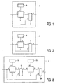
- a frequency divider 2 includes a divider cell 1 with input 5 and an output 7. This output 7 is connected to a first input 9 of a multiplexer 3.
- the multiplexer 3 has an output 13.
- the divider cell 1 has a bias control input 17, which is connected to a bias current controller 15. When the multiplexer 3 deselects its first input 9, the output 7 of the divider cell is not used by the circuit. Since the only purpose of the divider cell 1 is to divide an input signal that is present on the input 5 of the divider cell and make the resulting divided signal available to other parts of the divider via the multiplexer, it is no longer useful for the divider cell to divide the input signal.
- the divider cell 1 can be switched off by reducing the bias current for the divider cell to zero, which is supplied from the bias current supply 15 via the bias current input 17 to the divider cell 1.
- the multiplexer 3 can select another signal via a second input 11 and make this signal available on its output 13 when the output 7 of the divider cell 1 is deselected.
- the second input 11 of the multiplexer 3 is connected to the input 5 of the divider cell 1.
- the multiplexer 3 selects the output 7 of the divider cell 1, the divided input signal is made available on the output 13 of the multiplexer 3.
- the divider cell can be switched off by reducing the bias current supplied by the bias current controller 15 to zero.
- the signal that is made available on the output 13 of the multiplexer 3 is in this case the input signal of the divider cell 1.
- the multiplexer 3 makes it possible to switch the effective division factor between the input 5 of the divider cell and the output 13 of the multiplexer 3 between 1, when the input signal is directly selected by the multiplexer 3, and the division factor of the divider cell, when the output 7 of the divider cell is selected by the multiplexer 3.
- a frequency divider including more divider cells, multiplexers, and bias current controllers is shown in figure 3.
- an input 21 of a second divider cell 19 is connected to output 13 of the first multiplexer.
- the second divider cell 19 also includes a bias control input 27 which is connected to a second bias current supply 25.
- An output 23 of the second divider cell 19 is connected to a first input 31 of a second multiplexer 29.
- This second multiplexer 29 has an output 35 and a second input 33.
- This second input 33 is connected to the second input 11 of the first multiplexer 3.
- the input signal on the input 5 of the first divider cell is made available on the output 35 of the second multiplexer, realizing an effective division factor between the input 5 and the output 35 of 1. Both divider cells 1 and 19 can be switched off.
- the input signal is at least divided by the second divider cell 19, and, depending on the state of multiplexer 3, the input signal is also divided by the first divider cell 1. If the first divider cell 1 is deselected by the first multiplexer 3, the effective division factor is the division factor of the second divider cell 19, and the bias current that is supplied to the first divider cell 1 by the bias current controller can be reduced to zero. If the first divider cell 1 is selected by the first multiplexer 3, the effective division factor is the division factor of the first divider cell times the division factor of the second divider cell, and both divider cells 1 and 19 must be supplied with bias current by their corresponding bias current controllers 15 and 25.
- the bias current supplied to the second divider cell 19 by the second bias current controller 25 is reduced, thereby reducing the power consumption of the frequency divider 2.
- the second divider cell 19 effectively becomes the first divider cell which processes the input signal present on the input 5 of the first divider cell. Therefore, the operating frequency which the second divider cell 19 is designed for is the highest for the divider cells that remain operative, and the bias current is accordingly relatively high compared to the other active divider cells. A reduction of this relatively high bias current is an effective way to reduce power consumption by the frequency divider 2.
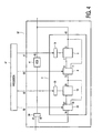
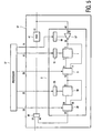
- a Phase Locked Loop (PLL) 37 is shown, which is controlled by a processor 57 and includes a frequency divider 2 according to the present invention.
- PLL Phase Locked Loop
- the PLL 37 includes a phase detector 39, which detects a phase difference between a reference signal on a reference input 51 and a divided VCO output signal on a compare input 49.
- the phase detector is connected to a Voltage Controlled Oscillator (VCO) 41 and provides the VCO 41 with information about the phase difference between the two input signals. Based on this information, the VCO 41 will generate an output signal which is made available on an output 43 of the VCO 41.
- the output 43 of the VCO is connected to an input 45 of the frequency divider 2.
- the input 45 of the frequency divider is connected to the input 5 of the first divider cell of the frequency divider 2.
- the VCO output signal on the output 43 of the VCO 41 is thus applied to the input 45 of the frequency divider 2 and, consequently, divided by the frequency divider 2, which results in a divided VCO output signal on the output 35 of the frequency divider 2.
- the division factor of the frequency divider 2 must be altered. This is achieved by controlling the multiplexers 3, 29 in the frequency divider 2 by signals provided by a processor, effectively allowing the VCO output signal to bypass the deselected divider cells. The processor thereby effectively controls the output frequency of the VCO 43 and thus of the PLL.
- the processor 57 Since the processor 57 controls the multiplexers 3, 29, it can also determine which divider cells can be switched off. Also, because the processor 57 knows the operating frequency of the PLL 37 and the state of the multiplexers 3, 29, it can determine which divider cell 1, 19 is operating and at what operating frequency. Therefore, the processor is able to determine a corresponding bias current that is appropriate for the divider cells.
- the processor 57 is connected to the bias current control 15 via a control port 61 and to the bias control 25 via a control port 55. Via these control ports 55, 61 the processor 57 can either completely switch off the bias current for the corresponding divider cell 1, 19, or reduce the bias current to suit the operating frequency of the corresponding divider cell 1, 19.
- Figure 5 shows the PLL 37, which includes an amplifier 67 with an input 63 connected to the input 45 of the frequency divider 2, and an output 65 connected to the input 5 of the first divider cell 1.
- This amplifier 67 amplifies the input signal, in this example the VCO output signal, and thus allows the frequency divider 2 to operate with lower level signals than of the amplifier were not present.
- the bias current of the amplifier 67 is dependent on the gain factor of the amplifier 67. When a low gain is sufficient to obtain an adequate signal level of the input signal for operation of the divider cell, the bias current of the amplifier 67 can be reduced. In this way it is possible to achieve a reduction of the power consumption of the frequency divider 2.
- the information about the signal level of the input signal of the divider cell 1, 19 can be obtained in several ways.
- a level meter can be used to measure the signal level, and adjust the amplification accordingly, similar to an automatic gain control circuit.
- the information is determined by the processor based on the operating frequency of the VCO 41, and the known characteristics of the VCO 41. The characteristics of a VCO often show a variation of output signal level, which depends on the operating frequency.
- the processor 57 can contain a lookup table or can use a mathematical relationship to determine what the expected signal level on the output 43 of the VCO 41 is, based on the actual operating frequency.
- the processor 57 can also determine what the required signal level of the various divider cells 1, 19 in the frequency divider 2 is, which can be frequency and divider cell dependent, and accordingly adjust the gain and bias current of the amplifier 67. This way the power consumption can be optimized depending on which divider cell is processing the signal on the output 65 of the amplifier 67.
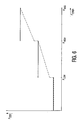
- Figure 6 shows the power consumption of the frequency divider.
- the solid lines in figure 6 show the effect of switching off a divider cell in the frequency divider.
- F max all cells have to be active and able to handle the maximum incoming frequencies.
- F oper of the input signal is reduced to F high .
- the first divider cell in the frequency divider is no longer needed and can be deselected or bypassed and switched off.
- the first divider cell By switching the first divider cell off, a drop of the power dissipation is achieved.
- the next divider cell can be deselected and switched off, effectively reducing the power consumption even more.
- the dotted line in figure 6 shows the effect of, in addition to switching appropriate divider cells off, reducing the bias current of a divider cell in relation to the operating frequency F oper of the divider cell.
- the first divider cell When the frequency of the input signal is Fmax, the first divider cell must operate at its highest frequency and the bias current is accordingly high. Together with the input frequency the bias current can be reduced as well.
- the operating frequency F oper is slightly higher than F high , the first divider cell is still operating and, therefore, still needs a certain amount of bias current.
- the first divider cell At frequency F high , the first divider cell can be deselected and switched off which results in a drop of the bias current.
- the second divider cell operates at the highest frequency in the system and its bias current can now advantageously be reduced in relation to the operating frequency F oper . This results in a reduction of the bias current along the dotted line, until F low is reached. At this point the second divider cell can also be switched off, resulting in a drop of the power consumption of the frequency divider.
Landscapes
- Stabilization Of Oscillater, Synchronisation, Frequency Synthesizers (AREA)
- Superheterodyne Receivers (AREA)
- Manipulation Of Pulses (AREA)
- Amplifiers (AREA)
- Noise Elimination (AREA)
Claims (10)
- Frequenzteiler mit einem einstellbaren Teilungsfaktor, mit einem Eingang und einer Teilerzelle mit einem Eingang zum Akzeptieren eines ersten Signals mit einer ersten Frequenz und einem Ausgang zum Ausliefern eines zweiten Signals mit einer zweiten Frequenz, und mit einem Leistungssteuermittel, das mit dem Frequenzteiler assoziiert ist zum Einstellen eines Vorspannungsstromes der Teilerzelle,
wobei der Frequenzteiler ein Multiplexmittel aufweist mit einem ersten Eingang zum Empfangen des zweiten Signals mit der zweiten Frequenz und mit einem zweiten Eingang zum Empfangen eines dritten Signals mit einer dritten Frequenz und mit einem Ausgang zum Ausliefern entweder des zweiten Signals oder des dritten Signals, wobei der erste Eingang des Multiplexmittels mit dem Ausgang der Teilerzelle verbunden ist, dadurch gekennzeichnet,
dass das Leistungssteuermittel wirksam ist zum Abschalten der Teilerzelle zum Reduzieren des Vorspannungsstromes der Teilerzelle zu Null, wenn der erste Eingang des Multiplexmittels abgewählt wird, und
dass das mit der Teilerzelle assoziierte Leistungssteuermittel wirksam ist zum Einstellen des Vorspannungsstromes der assoziierten Teilerzelle proportional zu einer Eingangsfrequenz der Teilerzelle, wenn die erste Eingabe des Multiplexermittels, das mit dem Ausgang dieser Teilerzelle verbunden ist, selektiert wird, zur allmählichen Reduktion der Leistung zwischen Leistungsreduktionsschritten, erzielt durch Abschaltung der Teilerzelle. - Frequenzteiler nach Anspruch 1, dadurch gekennzeichnet, dass der zweite Eingang des Multiplexermittels mit dem Eingang der Teilerzelle verbunden ist.
- Frequenzteiler nach Anspruch 1 oder 2 mit einer weiteren Teilerzelle, die als zweite Teilerzelle bezeichnet wird, mit einem Eingang und einem Ausgang, dadurch gekennzeichnet, dass der Eingang der zweiten Verteilerzelle mit dem Ausgang des Multiplexermittels verbunden ist.
- Frequenzteiler nach Anspruch 3, mit einem weiteren Leistungssteuermittel, das als das zweite Leistungssteuermittel bezeichnet wird, assoziiert mit der zweiten Teilerzelle, zum Einstellen eines Vorspannungsstromes der zweiten Teilerzelle, dadurch gekennzeichnet, dass der Frequenzteiler ein weiteres Multiplexermittel aufweist, das als das zweites Multiplexermittel bezeichnet wird , mit einem ersten Eingang und einem zweiten Eingang und mit einem Ausgang, wobei der erste Eingang des zweiten Multiplexermittels mit dem Ausgang der zweiten Teilerzelle verbunden ist und wobei der zweite Eingang des zweiten Multiplexermittels mit dem zweiten Eingang des Multiplexermittels verbunden ist und dass das zweite Leistungssteuermittel wirksam ist zum Reduzieren des Vorspannungsstromes der zweiten Teilerzelle zu Null, wenn der erste Eingang des zweiten Multiplexermittels abgewählt wird.
- Frequenzteiler nach Anspruch 1,2,3 oder 4, mit einem Eingangsverstärker mit einem Verstärkervorspannungsstrom und mit einem Eingang, der mit dem Eingang des Frequenzteilers versehen ist, und mit einem Ausgang, der mit dem Eingang der Teilerzelle verbunden ist,
dadurch gekennzeichnet, dass ein drittes Leistungssteuermittel wirksam ist zum Einstellen des Verstärkervorspannungsstromes des Eingangsverstärkers, und zwar abhängig von einer Eingangsfrequenz des Eingangsverstärkers. - Frequenzteiler nach Anspruch 1, 2, 3, 4 oder 5, dadurch gekennzeichnet, dass der Frequenzteiler mit einem spannungsgeregelten Oszillator (VCO) gekoppelt ist und das Leistungssteuermittel dazu vorgesehen ist, die Eingangsfrequenz der Teilerzelle auf Basis einer wirklichen Operationsfrequenz des spannungsgeregelten Oszillators (VCO) zu ermitteln.
- Frequenzteiler nach Anspruch 1, 2, 3, 4, 5, oder 6, dadurch gekennzeichnet, dass wenigstens eine Leistungssteuerung mit einem Prozessor verbunden ist, wobei dieser Prozessor wirksam ist zum Einstellen des Leistungssteuermittels, wenn die assoziierte Teilerzelle abgewählt wird.
- Phasenverriegelte Schleife mit einem VCO und einem Frequenzteiler nach Anspruch 1, 2, 3, 4, 5, 6 oder 7.
- Phasenverriegelte Schleife nach Anspruch 8, dadurch gekennzeichnet, dass ein Mikroprozessor wirksam ist zum Steuern des VCOs und wenigstens des Leistungssteuermittels des Frequenzteilers.
- Mobiltelefon mit einem Frequenzteiler nach Anspruch 1, 2, 3, 4, 5, 6, oder 7.
Priority Applications (1)
| Application Number | Priority Date | Filing Date | Title |
|---|---|---|---|
| EP01927915A EP1281237B1 (de) | 2000-05-01 | 2001-04-13 | Frequenzteiler mit veränderbarem teilverhältnis und angepasstem leistungsverbrauch |
Applications Claiming Priority (4)
| Application Number | Priority Date | Filing Date | Title |
|---|---|---|---|
| EP00201561 | 2000-05-01 | ||
| EP00201561 | 2000-05-01 | ||
| PCT/EP2001/004321 WO2001084710A1 (en) | 2000-05-01 | 2001-04-13 | Power adaptive frequency divider |
| EP01927915A EP1281237B1 (de) | 2000-05-01 | 2001-04-13 | Frequenzteiler mit veränderbarem teilverhältnis und angepasstem leistungsverbrauch |
Publications (2)
| Publication Number | Publication Date |
|---|---|
| EP1281237A1 EP1281237A1 (de) | 2003-02-05 |
| EP1281237B1 true EP1281237B1 (de) | 2007-09-26 |
Family
ID=8171436
Family Applications (1)
| Application Number | Title | Priority Date | Filing Date |
|---|---|---|---|
| EP01927915A Expired - Lifetime EP1281237B1 (de) | 2000-05-01 | 2001-04-13 | Frequenzteiler mit veränderbarem teilverhältnis und angepasstem leistungsverbrauch |
Country Status (9)
| Country | Link |
|---|---|
| US (1) | US6489818B2 (de) |
| EP (1) | EP1281237B1 (de) |
| JP (1) | JP2003533084A (de) |
| KR (1) | KR20020029872A (de) |
| CN (1) | CN1276579C (de) |
| AT (1) | ATE374450T1 (de) |
| DE (1) | DE60130648T2 (de) |
| TW (1) | TW527763B (de) |
| WO (1) | WO2001084710A1 (de) |
Families Citing this family (12)
| Publication number | Priority date | Publication date | Assignee | Title |
|---|---|---|---|---|
| US8320845B2 (en) * | 2003-03-18 | 2012-11-27 | Telefonaktiebolaget L M Ericsson (Publ) | Radio transmitter |
| DE60300716T2 (de) * | 2003-03-18 | 2005-10-20 | Telefonaktiebolaget Lm Ericsson (Publ) | Funksender |
| KR100638893B1 (ko) | 2006-01-02 | 2006-10-27 | 삼성전기주식회사 | 바디 바이어스 조절을 이용한 쿼드러처 프리스케일러 |
| EP1959562B1 (de) * | 2007-02-15 | 2010-12-08 | STMicroelectronics Srl | Volldifferentieller Demodulator mit variabler Verstärkung und Demodulationsverfahren eines Signals |
| JP4768645B2 (ja) * | 2007-02-16 | 2011-09-07 | パナソニック株式会社 | Pll回路、およびそれを備えた無線装置 |
| FI20075715A0 (fi) * | 2007-10-09 | 2007-10-09 | Nokia Corp | Taajuusjakajan konfiguraatio |
| JP5531969B2 (ja) * | 2011-01-12 | 2014-06-25 | ミツミ電機株式会社 | 発振回路 |
| US9157950B2 (en) * | 2011-04-18 | 2015-10-13 | International Business Machines Corporation | Loop parameter sensor using repetitive phase errors |
| CN102291119B (zh) * | 2011-06-07 | 2017-08-08 | 中兴通讯股份有限公司 | 分频装置及方法 |
| US8406371B1 (en) | 2012-01-04 | 2013-03-26 | Silicon Laboratories Inc. | Programmable divider circuitry for improved duty cycle consistency and related systems and methods |
| US20150091620A1 (en) * | 2013-10-01 | 2015-04-02 | Lsi Corporation | Reducing current variation when switching clocks |
| JP7261159B2 (ja) | 2017-06-08 | 2023-04-19 | 株式会社レゾナック | エッチング方法 |
Family Cites Families (13)
| Publication number | Priority date | Publication date | Assignee | Title |
|---|---|---|---|---|
| JPS59208945A (ja) * | 1983-05-13 | 1984-11-27 | Nec Corp | プリスケ−ラ回路 |
| JPS62117408A (ja) * | 1985-11-18 | 1987-05-28 | Casio Comput Co Ltd | オ−トチユ−ニング装置 |
| JPS6318721A (ja) * | 1986-07-11 | 1988-01-26 | Hitachi Ltd | 信号処理回路 |
| JP2642408B2 (ja) * | 1988-05-18 | 1997-08-20 | 三菱電機株式会社 | 分周回路装置 |
| JPH05206850A (ja) * | 1992-01-23 | 1993-08-13 | Nec Corp | Pll周波数シンセサイザ |
| US5416446A (en) * | 1992-12-08 | 1995-05-16 | At&T Corp. | Digital programmable frequency generator |
| JPH07105739B2 (ja) * | 1993-06-08 | 1995-11-13 | 日本電気株式会社 | 受信機 |
| FR2734966B1 (fr) * | 1995-05-31 | 1997-08-14 | Sgs Thomson Microelectronics | Diviseur programmable rapide |
| US5815694A (en) * | 1995-12-21 | 1998-09-29 | International Business Machines Corporation | Apparatus and method to change a processor clock frequency |
| US5859890A (en) * | 1997-02-26 | 1999-01-12 | Motorola, Inc. | Dual modulus prescaler |
| US6009139A (en) * | 1998-06-19 | 1999-12-28 | International Business Machines Corporation | Asynchronously programmable frequency divider circuit with a symmetrical output |
| JP3654153B2 (ja) * | 2000-07-26 | 2005-06-02 | 株式会社デンソー | クロック信号発生装置及びマイクロコンピュータ |
| JP3508762B2 (ja) * | 2001-12-18 | 2004-03-22 | セイコーエプソン株式会社 | 分周回路 |
-
2001
- 2001-04-12 TW TW090108788A patent/TW527763B/zh not_active IP Right Cessation
- 2001-04-13 AT AT01927915T patent/ATE374450T1/de not_active IP Right Cessation
- 2001-04-13 JP JP2001581416A patent/JP2003533084A/ja active Pending
- 2001-04-13 CN CNB018011632A patent/CN1276579C/zh not_active Expired - Fee Related
- 2001-04-13 KR KR1020017016945A patent/KR20020029872A/ko not_active Ceased
- 2001-04-13 EP EP01927915A patent/EP1281237B1/de not_active Expired - Lifetime
- 2001-04-13 WO PCT/EP2001/004321 patent/WO2001084710A1/en not_active Ceased
- 2001-04-13 DE DE60130648T patent/DE60130648T2/de not_active Expired - Lifetime
- 2001-04-30 US US09/846,600 patent/US6489818B2/en not_active Expired - Lifetime
Also Published As
| Publication number | Publication date |
|---|---|
| KR20020029872A (ko) | 2002-04-20 |
| WO2001084710A1 (en) | 2001-11-08 |
| DE60130648D1 (de) | 2007-11-08 |
| US20010035781A1 (en) | 2001-11-01 |
| EP1281237A1 (de) | 2003-02-05 |
| DE60130648T2 (de) | 2008-07-17 |
| CN1276579C (zh) | 2006-09-20 |
| TW527763B (en) | 2003-04-11 |
| JP2003533084A (ja) | 2003-11-05 |
| US6489818B2 (en) | 2002-12-03 |
| CN1372719A (zh) | 2002-10-02 |
| ATE374450T1 (de) | 2007-10-15 |
Similar Documents
| Publication | Publication Date | Title |
|---|---|---|
| EP1281237B1 (de) | Frequenzteiler mit veränderbarem teilverhältnis und angepasstem leistungsverbrauch | |
| EP0944172A2 (de) | Phasenregelschleife zur Erzeugung eines Ausgangssignals in zwei oder mehr Frequenzbändern | |
| EP1277286B9 (de) | Persönliche kommunikationsanlage mit gps empfänger und gemeinsamer taktquelle | |
| CN111884666A (zh) | 一种采用锁相环复用的多模多通道射频接收机芯片 | |
| US6411660B1 (en) | Device for reducing lock-up time of Frequency synthesizer | |
| CN112234981A (zh) | 数据与时钟恢复电路 | |
| JPH1155108A (ja) | プレスケーラとその後に続くプログラマブルカウンタを有する周波数分割器、および対応するプレスケーラならびに周波数合成器 | |
| US7480496B2 (en) | High-frequency receiver and portable device using the same | |
| KR20010093099A (ko) | 위상 동기 루프 주파수 생성 회로 및 그 회로를 사용하는수신기 | |
| US6943639B2 (en) | Arrangement for low power clock generation | |
| US7816954B2 (en) | Circuit configuration of a frequency divider | |
| EP1514343A1 (de) | Anordnung zur taktgeneration mit niedriger leistung | |
| JP3917592B2 (ja) | 周波数シンセサイザ | |
| US20040198418A1 (en) | Digital signal transceiver | |
| US7515002B2 (en) | Frequency synthesizer for dual mode receiver | |
| EP1656741B1 (de) | Bereitstellung von lokalen oszillatorsignalen | |
| EP1629600B1 (de) | Vorrichtung zur versorgung eines oscillationssignals zu einer last | |
| JP4625030B2 (ja) | 通信システム | |
| KR20010102925A (ko) | Pll 회로에 의한 주파수 발생 방법 | |
| JP2002009617A (ja) | Pll回路 | |
| JP2002261603A (ja) | Pll回路及びそれを用いた通信機 | |
| JP2003069428A (ja) | マルチバンドpll回路 | |
| JP2007281806A (ja) | マルチモード対応周波数シンセサイザ | |
| JPH01314427A (ja) | 周波数シンセサイザ |
Legal Events
| Date | Code | Title | Description |
|---|---|---|---|
| PUAI | Public reference made under article 153(3) epc to a published international application that has entered the european phase |
Free format text: ORIGINAL CODE: 0009012 |
|
| 17P | Request for examination filed |
Effective date: 20021202 |
|
| AK | Designated contracting states |
Designated state(s): AT BE CH CY DE DK ES FI FR GB GR IE IT LI LU MC NL PT SE TR |
|
| 17Q | First examination report despatched |
Effective date: 20041119 |
|
| APBN | Date of receipt of notice of appeal recorded |
Free format text: ORIGINAL CODE: EPIDOSNNOA2E |
|
| APBR | Date of receipt of statement of grounds of appeal recorded |
Free format text: ORIGINAL CODE: EPIDOSNNOA3E |
|
| APAF | Appeal reference modified |
Free format text: ORIGINAL CODE: EPIDOSCREFNE |
|
| APBV | Interlocutory revision of appeal recorded |
Free format text: ORIGINAL CODE: EPIDOSNIRAPE |
|
| GRAP | Despatch of communication of intention to grant a patent |
Free format text: ORIGINAL CODE: EPIDOSNIGR1 |
|
| APBT | Appeal procedure closed |
Free format text: ORIGINAL CODE: EPIDOSNNOA9E |
|
| GRAS | Grant fee paid |
Free format text: ORIGINAL CODE: EPIDOSNIGR3 |
|
| RAP1 | Party data changed (applicant data changed or rights of an application transferred) |
Owner name: NXP B.V. |
|
| GRAA | (expected) grant |
Free format text: ORIGINAL CODE: 0009210 |
|
| AK | Designated contracting states |
Kind code of ref document: B1 Designated state(s): AT BE CH CY DE DK ES FI FR GB GR IE IT LI LU MC NL PT SE TR |
|
| REG | Reference to a national code |
Ref country code: GB Ref legal event code: FG4D |
|
| REG | Reference to a national code |
Ref country code: CH Ref legal event code: EP |
|
| REF | Corresponds to: |
Ref document number: 60130648 Country of ref document: DE Date of ref document: 20071108 Kind code of ref document: P |
|
| REG | Reference to a national code |
Ref country code: IE Ref legal event code: FG4D |
|
| PG25 | Lapsed in a contracting state [announced via postgrant information from national office to epo] |
Ref country code: FI Free format text: LAPSE BECAUSE OF FAILURE TO SUBMIT A TRANSLATION OF THE DESCRIPTION OR TO PAY THE FEE WITHIN THE PRESCRIBED TIME-LIMIT Effective date: 20070926 |
|
| PG25 | Lapsed in a contracting state [announced via postgrant information from national office to epo] |
Ref country code: AT Free format text: LAPSE BECAUSE OF FAILURE TO SUBMIT A TRANSLATION OF THE DESCRIPTION OR TO PAY THE FEE WITHIN THE PRESCRIBED TIME-LIMIT Effective date: 20070926 |
|
| NLV1 | Nl: lapsed or annulled due to failure to fulfill the requirements of art. 29p and 29m of the patents act | ||
| PG25 | Lapsed in a contracting state [announced via postgrant information from national office to epo] |
Ref country code: BE Free format text: LAPSE BECAUSE OF FAILURE TO SUBMIT A TRANSLATION OF THE DESCRIPTION OR TO PAY THE FEE WITHIN THE PRESCRIBED TIME-LIMIT Effective date: 20070926 |
|
| REG | Reference to a national code |
Ref country code: CH Ref legal event code: PL |
|
| PG25 | Lapsed in a contracting state [announced via postgrant information from national office to epo] |
Ref country code: NL Free format text: LAPSE BECAUSE OF FAILURE TO SUBMIT A TRANSLATION OF THE DESCRIPTION OR TO PAY THE FEE WITHIN THE PRESCRIBED TIME-LIMIT Effective date: 20070926 Ref country code: LI Free format text: LAPSE BECAUSE OF FAILURE TO SUBMIT A TRANSLATION OF THE DESCRIPTION OR TO PAY THE FEE WITHIN THE PRESCRIBED TIME-LIMIT Effective date: 20070926 Ref country code: GR Free format text: LAPSE BECAUSE OF FAILURE TO SUBMIT A TRANSLATION OF THE DESCRIPTION OR TO PAY THE FEE WITHIN THE PRESCRIBED TIME-LIMIT Effective date: 20071227 Ref country code: ES Free format text: LAPSE BECAUSE OF FAILURE TO SUBMIT A TRANSLATION OF THE DESCRIPTION OR TO PAY THE FEE WITHIN THE PRESCRIBED TIME-LIMIT Effective date: 20080106 Ref country code: CH Free format text: LAPSE BECAUSE OF FAILURE TO SUBMIT A TRANSLATION OF THE DESCRIPTION OR TO PAY THE FEE WITHIN THE PRESCRIBED TIME-LIMIT Effective date: 20070926 |
|
| ET | Fr: translation filed | ||
| PG25 | Lapsed in a contracting state [announced via postgrant information from national office to epo] |
Ref country code: PT Free format text: LAPSE BECAUSE OF FAILURE TO SUBMIT A TRANSLATION OF THE DESCRIPTION OR TO PAY THE FEE WITHIN THE PRESCRIBED TIME-LIMIT Effective date: 20080226 |
|
| PG25 | Lapsed in a contracting state [announced via postgrant information from national office to epo] |
Ref country code: SE Free format text: LAPSE BECAUSE OF FAILURE TO SUBMIT A TRANSLATION OF THE DESCRIPTION OR TO PAY THE FEE WITHIN THE PRESCRIBED TIME-LIMIT Effective date: 20071226 |
|
| PG25 | Lapsed in a contracting state [announced via postgrant information from national office to epo] |
Ref country code: DK Free format text: LAPSE BECAUSE OF FAILURE TO SUBMIT A TRANSLATION OF THE DESCRIPTION OR TO PAY THE FEE WITHIN THE PRESCRIBED TIME-LIMIT Effective date: 20070926 |
|
| PLBE | No opposition filed within time limit |
Free format text: ORIGINAL CODE: 0009261 |
|
| STAA | Information on the status of an ep patent application or granted ep patent |
Free format text: STATUS: NO OPPOSITION FILED WITHIN TIME LIMIT |
|
| 26N | No opposition filed |
Effective date: 20080627 |
|
| PG25 | Lapsed in a contracting state [announced via postgrant information from national office to epo] |
Ref country code: MC Free format text: LAPSE BECAUSE OF NON-PAYMENT OF DUE FEES Effective date: 20080430 |
|
| PG25 | Lapsed in a contracting state [announced via postgrant information from national office to epo] |
Ref country code: IE Free format text: LAPSE BECAUSE OF NON-PAYMENT OF DUE FEES Effective date: 20080414 |
|
| PG25 | Lapsed in a contracting state [announced via postgrant information from national office to epo] |
Ref country code: CY Free format text: LAPSE BECAUSE OF FAILURE TO SUBMIT A TRANSLATION OF THE DESCRIPTION OR TO PAY THE FEE WITHIN THE PRESCRIBED TIME-LIMIT Effective date: 20070926 |
|
| PG25 | Lapsed in a contracting state [announced via postgrant information from national office to epo] |
Ref country code: LU Free format text: LAPSE BECAUSE OF NON-PAYMENT OF DUE FEES Effective date: 20080413 |
|
| PG25 | Lapsed in a contracting state [announced via postgrant information from national office to epo] |
Ref country code: TR Free format text: LAPSE BECAUSE OF FAILURE TO SUBMIT A TRANSLATION OF THE DESCRIPTION OR TO PAY THE FEE WITHIN THE PRESCRIBED TIME-LIMIT Effective date: 20070926 |
|
| PG25 | Lapsed in a contracting state [announced via postgrant information from national office to epo] |
Ref country code: IT Free format text: LAPSE BECAUSE OF NON-PAYMENT OF DUE FEES Effective date: 20080430 |
|
| REG | Reference to a national code |
Ref country code: FR Ref legal event code: PLFP Year of fee payment: 15 |
|
| REG | Reference to a national code |
Ref country code: FR Ref legal event code: PLFP Year of fee payment: 16 |
|
| REG | Reference to a national code |
Ref country code: FR Ref legal event code: PLFP Year of fee payment: 17 |
|
| REG | Reference to a national code |
Ref country code: FR Ref legal event code: PLFP Year of fee payment: 18 |
|
| PGFP | Annual fee paid to national office [announced via postgrant information from national office to epo] |
Ref country code: GB Payment date: 20180321 Year of fee payment: 18 |
|
| PGFP | Annual fee paid to national office [announced via postgrant information from national office to epo] |
Ref country code: FR Payment date: 20180322 Year of fee payment: 18 |
|
| PGFP | Annual fee paid to national office [announced via postgrant information from national office to epo] |
Ref country code: DE Payment date: 20180320 Year of fee payment: 18 |
|
| REG | Reference to a national code |
Ref country code: DE Ref legal event code: R119 Ref document number: 60130648 Country of ref document: DE |
|
| GBPC | Gb: european patent ceased through non-payment of renewal fee |
Effective date: 20190413 |
|
| PG25 | Lapsed in a contracting state [announced via postgrant information from national office to epo] |
Ref country code: DE Free format text: LAPSE BECAUSE OF NON-PAYMENT OF DUE FEES Effective date: 20191101 Ref country code: GB Free format text: LAPSE BECAUSE OF NON-PAYMENT OF DUE FEES Effective date: 20190413 |
|
| PG25 | Lapsed in a contracting state [announced via postgrant information from national office to epo] |
Ref country code: FR Free format text: LAPSE BECAUSE OF NON-PAYMENT OF DUE FEES Effective date: 20190430 |