EP1267507B1 - A method and apparatus for transmitting and receiving multiplex tributary signals - Google Patents
A method and apparatus for transmitting and receiving multiplex tributary signals Download PDFInfo
- Publication number
- EP1267507B1 EP1267507B1 EP01305212A EP01305212A EP1267507B1 EP 1267507 B1 EP1267507 B1 EP 1267507B1 EP 01305212 A EP01305212 A EP 01305212A EP 01305212 A EP01305212 A EP 01305212A EP 1267507 B1 EP1267507 B1 EP 1267507B1
- Authority
- EP
- European Patent Office
- Prior art keywords
- signal
- tributary
- phase difference
- phase
- signals
- Prior art date
- Legal status (The legal status is an assumption and is not a legal conclusion. Google has not performed a legal analysis and makes no representation as to the accuracy of the status listed.)
- Expired - Lifetime
Links
- 238000000034 method Methods 0.000 title claims description 8
- 150000001875 compounds Chemical group 0.000 claims description 43
- 238000010586 diagram Methods 0.000 description 4
- 238000005259 measurement Methods 0.000 description 4
- 238000004364 calculation method Methods 0.000 description 3
- 230000001788 irregular Effects 0.000 description 3
- 238000013139 quantization Methods 0.000 description 3
- 230000015572 biosynthetic process Effects 0.000 description 1
- 238000010276 construction Methods 0.000 description 1
- 238000005516 engineering process Methods 0.000 description 1
- 230000006870 function Effects 0.000 description 1
- 238000011084 recovery Methods 0.000 description 1
Images

Classifications
-
- H—ELECTRICITY
- H04—ELECTRIC COMMUNICATION TECHNIQUE
- H04J—MULTIPLEX COMMUNICATION
- H04J3/00—Time-division multiplex systems
- H04J3/02—Details
- H04J3/06—Synchronising arrangements
- H04J3/07—Synchronising arrangements using pulse stuffing for systems with different or fluctuating information rates or bit rates
- H04J3/076—Bit and byte stuffing, e.g. SDH/PDH desynchronisers, bit-leaking
-
- H—ELECTRICITY
- H04—ELECTRIC COMMUNICATION TECHNIQUE
- H04J—MULTIPLEX COMMUNICATION
- H04J3/00—Time-division multiplex systems
- H04J3/02—Details
- H04J3/06—Synchronising arrangements
- H04J3/0635—Clock or time synchronisation in a network
- H04J3/0685—Clock or time synchronisation in a node; Intranode synchronisation
Definitions
- the invention relates to a method and an apparatus for transmitting and receiving a plurality of individual tributary signals in multiplex form via a common line.
- a data line can carry a plurality of signals originating from a plurality of individual sources.
- a plurality of signals of nominal the same frequency termed “tributary signals” are multiplexed for being transmitted via the common line as a “compound signal”.
- the multiplexed signals are mapped into the compound signal which has a frame structure and is of a higher data rate than the sum of the tributary frequences.
- the compound signal, received at the receiver is demultiplexed.
- the individual tributary signals so obtained should be identical to the original tributary signals before being multiplexed at the transmitter. This means that the frequency of each demultiplexed tributary signal (“the recovered clock”) should be identical to the frequency of the original signal.
- additional bits are used. This offers the possibility to transmit initial tributary signals of somewhat different frequencies. Some of the additional bits are used to transmit control information needed for the rate adaption of these tributary signals. Some of the additional bits can also be used to transmit some other additional information.
- the additional bits are put in a fixed position into the framed compound signal. Rate adaption is made by a stuffing procedure. To that end, gaps are provided in fixed frame positions, wherein information data can be inserted, or which can be left empty. When the initial tributary frequency is lower than the nominal rate, these gaps remain empty (positive stuffing). When the initial tributary frequency is higher than the nominal rate, some of the bits are inserted in the empty positions (negative stuffing).
- the tributary signals which are adapted in rate, are multiplexed, that is, the bits or bytes of the signals are interleaved and transmitted to the receiver through the common line.
- the signals are demultiplexed.
- phase information transmitted with the compound signal is used, namely the phase difference between the compound signal and the tributary signal. This phase difference is transmitted in the gaps provided in the fixed frame positions and makes no big harm.
- the stuffing information means a rough quantization of the phase which causes wander and jitter of the recovered frequency or clock.
- EP-A-1067722 and United States patent US-A-5 263 057 are referred to as background. It is known from EP-A-1067722 to provide a method of transmitting and receiving a plurality of individual tributary signals in multiplex form via a common line, including the steps of: converting, at the transmitting end, the individual tributary signals, each of which having a similar initial frequency, into a compound signal having a frame structure with a common data rate, and retrieving, at the receiving end, from the compound signal each individual tributary signal.
- the present invention is characterised over the disclosure of EP-A-1067722 in that at the transmitting end, a phase information signal portion including a respective phase difference between each tributary signal and the compound signal is formed and inserted into the compound signal in the form of respective coded bits, and, at the receiving end, the initial frequency of each tributary signal is recovered from the phase information signal portion included in the respective coded bits belonging to the respective tributary signals, wherein an auxiliary clock is used when calculating the phase difference between the compound signal and the tributary signal.
- the invention in its preferred embodiments holds wander and jitter in the compound signal as low as possible.
- phase difference between the compound signal and the tributary signal is accurately calculated.
- This calculated phase difference is coded preferably by a binary number and is transmitted in dedicated bytes of the compound line signal.
- the initial frequency of each tributary signal is recovered. For that purpose, the phase information transmitted is used.
- the accurate calculation of the phase difference is obtained by using an auxiliary clock at the transmitter. Furthermore, the mean value of the phase difference is calculated for a fixed time interval where the mean value is obtained by an integrator.
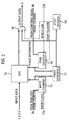
- Fig. 1 shows a transmitter for inputting four tributary signals 1, 2, 3, 4 and outputting a line compound signal 5 which includes all data of the tributary signals and some control data and may have a frequency of say 10 GHz.
- Each tributary signal is delivered to a respective synchronizer 6 which prepares a rate adapted tributary signal 61 for being interleaved by a multiplexer 7 with the remaining rate adapted tributary signals 62, 63, and 64.
- the multiplexer 7 composes the data of the tributary signals 61 to 64 and delivers such composed signal to a frame constructor 8 which finally outputs the line compound signal via line 5.
- the frame constructor is controlled by a frame counter 9 and a system clock 10 having the frequency of the line compound signal.
- the system clock 10 is also delivered to the frame counter 9 and a phase-locked loop 11 which outputs an internally generated auxiliary clock.
- the output of the phase-locked loop 11 and a further auxiliary clock 12 are delivered to a gate 13 so that the auxiliary clock 12 can be made effective for each of the synchronizers 6.
- the auxiliary clock 12 is an uncorrelated cycle to the writing cycle and the reading cycle and is used to obtain a higher resolution of the phase difference between signals.
- Cycle adaption which is aimed at, makes it necessary to use a plurality of gate functions. For this reason, cycle adaption is realized in CMOS technology which allows a relative low frequency of say 78 MHz (in relation to 10 GHz of the compound signal 5). Therefore, the serial data are transformed to parallel data and are written with this low frequency into a memory and read out with a similar low frequence from the memory.
- Fig. 2 shows particulars of each synchronizer 6.
- Input data from one of the tributary signals 1 through 4 is delivered to a FIFO register 14 which is controlled by a write counter 15 and a read counter 16.
- the write counter 15 is operated by a write clock 12a and receives the numbers of the bits in the tributary signal via line 9a.
- the read counter 16 is operated by a read clock 12b and receives the number of the bits from the compound signal through line 9b.
- the register 14 is an elastic store which provides write-in positions (write address) for the data bits of the respective tributary signals 1 to 4, and read-out positions (read address) for reading out these data bits together with bit gaps as provided by the frame structure of the compound signal.
- a phase difference unit 17 is provided which by the operation of the write counter 15 and the read counter 16, forms or calculates a phase difference between each tributary signal and the compound signal.
- the phase difference is formed between write and read address of register 14.
- the resolution obtained with this measurement corresponds to the cycle time of the writing cycle or the reading cycle, that is, phase difference measurement is made syncronously with one of these cycles.
- this resolution is not sufficient to fulfil the requirements as to jitter at the output of the tributary signal.
- the phase difference between write and read address is changing continuously, and measurement is only a rough quantization of this phase difference. This is the reason why the auxiliary clock 12 is used which is uncorrelated to the writing and reading cycle and allows measurement at fine stepped times.
- the auxiliary clock 12 is drifting slowly, so that, in a measuring period, the clock shifts through all possible positions during a cycle time period of the writing or reading cycle. Additionally, an average value is formed for a defined measuring period which corresponds to the distance between two stuffing positions, i. e. the measured values are integrated across the measuring time. The average value obtained allows the decision: stuffing positively, stuffing negatively or no stuffing. Formation of such average value allows to calculate the influence of the gaps which, due to the frame construction, occur regularly.
- the phase difference unit 17 makes a binary number from the average phase difference and delivers such coded phase information to a data output gate 18.
- the coded phase information is also delivered to a stuff decision unit 19 which has outputs connected to the read counter 16 and the output data gate 18.
- the auxiliary clock 12 with its portions write clock 12a and read clock 12b allows the accurate calculation of the phase difference between the line signal 5 and the tributary signals 1, 2, 3, and 4, respectively.
- the phase difference unit 17 includes the integrator referred-to above which, for a fixed time interval, forms the mean or average value of the phase difference which is the basis for calculating, the phase difference between line signal and tributary signal.
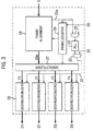
- Fig. 3 shows a receiver for four tributary data outputs 21, 22, 23, 24. These output lines 21 through 24 belong to respective desynchronizers 26 which are connected to a demultiplexer 27.
- the demultiplexer 27 is controlled by a frame alignment circuit 28 which is interconnected with a frame counter 29.
- System clock 30 is connected to frame counter 29 and a gate 25 which is also connected to the frame alignment circuit through a recovered clock line 25a.
- the gate 25 generates internally an auxiliary clock which is delivered to a phase-locked loop 31 which outputs to a gate 33 having a second input connected to a further auxiliary clock 32.
- the gated auxiliary clock is also connected to each desynchronizer 26.
- Line 5 delivers the compound signal carrying the data of the tributary signals and also additional bits to the frame alignment circuit 28 which firstly outputs the data of the composed signal and secondly the recovered clock 25a of the compound signal.
- the recovered clock 25a is used in the frame counter 29 to decide when a frame begins and ends.
- the demultiplexer 27 receives the data of the composed signal 28a and is controlled by the frame counter 29 so as to deliver the appropriate rate adapted data 71 to 74 to the respective desynchronizer 26 in the adapted rate.
- the auxiliary clock 32 is used to reconstruct the initial frequency or rate of the respective desynchonizer 26 so that each tributary data output 21, 22, 23, or 24 has a frequency which is exactly the same as the initial frequency of the signal.
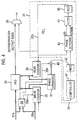
- Fig. 4 shows a desynchronizer circuit 26.
- Data from the demultiplexer 27 on line 27a get into a FIFO register 34, to which a write counter 35 and a read counter 36 as well as a phase difference unit 37 are connected.
- FIFO register 34 is an elastic store having write-in positions (write address) for the compound signal received, and read-out positions (read address) for the data bits of the respective tributary signals.
- Input line 27a is also connected to a phase and stuff information unit 39 which has a second input 29a from compound signal frame counter 29.
- Phase and stuff information unit 39 has a first output 39a for delivering stuff information to the write counter 35 and a second output 39b for delivering phase information to a summing member 40 which has a second input from the phase difference unit 37.
- the output of the summing member 40 is the input of the phase-locked loop 31 which includes a controller 41, a numeric controlled oscillator 42, a phase detector 43, a filter 44 and a voltage-controlled oscillator 45.
- the output of the voltage-controlled oscillator is the read clock 32b and is also used as the tributary clock to an output data gate 38.
- the data of the composed signal reaching the demultiplexer 27 from the frame alignment circuit 28 are demultiplexed, so that signals 71 to 74 containing the additional bits in an adapted rate are obtained in succession in the several desynchronizers 26.
- the additional bits in the compound signal are read out from the rate adapted data stream of the tributary signal 27a into unit 39, whereas all bits in the compound signal are written into elastic store 34.
- the coded phase information taken up from unit 39 is used for an accurate calculation of the phase difference between the write and read address of the elastic store 34. The whole phase difference is calculated in phase difference unit 37.
- the whole phase difference has several portions: stuffing information (which is a rough quantization of the phase course, and is only transferred when actually a stuffing operation is made), synchronizer phase difference between write and read addresses (which has been calculated at the synchronizer and is transferred to the desynchronizer with specific bytes. This value is transferred regularly, one time per stuffing position independently from whether there is a stuffing operation, or not), and desynchronizer phase difference between write and read addresses (calculated at the desynchronizer as a mean or average value, in the same manner as at the synchronizer).
- the whole phase difference is the addition of these portion and is added to the phase course of the system clock or cycle of the respective channel or tributary signal (when frame gaps removed) so as to yield the original phase course of the respective channel.
- phase information as well as phase difference calculated is further processed for such clock recovery in the phase-locked loop 31.
- the loop includes a numeric controlled oscillator 42 so that the output signal thereof takes the initial frequency of the respective tributary signal 1, 2, 3, or 4.
- the phase-locked loop 31 is responsive for delivering the clock with the correct phase relation.
- any phase deviation from the phase of an ideal clock of the same frequency is wander and jitter.
- wander and jitter are kept low by the procedure described above, since the tributary clock on line 32b is recovered from the clock of the demultiplexed signal from which the gaps contained in the compound signals have been removed by virtue of the phase-locked loop 31.
- the additional bits in the regular gaps of the frame structure of the compound signal produce only low values of phase deviation, since the phase-locked loop 31 has a low cut-off frequency.
- irregular gaps as occurring with stuffing produce irregular phase steps at the input of the phase-locked loop 31. This will produce big phase changes at the output of the phase-locked loop.
- the transmitted phase difference is used when recovering the clock in the receiver so that the clock produced in the phase-locked loop 31 is a clock with the desired phase for each tributary signal.
- the phase at the output of summing member 40 contains no more irregular and big phase steps.
Landscapes
- Engineering & Computer Science (AREA)
- Computer Networks & Wireless Communication (AREA)
- Signal Processing (AREA)
- Time-Division Multiplex Systems (AREA)
- Synchronisation In Digital Transmission Systems (AREA)
Priority Applications (5)
| Application Number | Priority Date | Filing Date | Title |
|---|---|---|---|
| EP01305212A EP1267507B1 (en) | 2001-06-15 | 2001-06-15 | A method and apparatus for transmitting and receiving multiplex tributary signals |
| DE60108728T DE60108728T2 (de) | 2001-06-15 | 2001-06-15 | Verfahren und ein Vorrichtung zum Übersenden und Empfangen gemultiplexter untergeordneter Signale |
| CA002381834A CA2381834A1 (en) | 2001-06-15 | 2002-04-16 | A method and apparatus for transmitting and receiving multiplex tributary signals |
| US10/166,897 US7254207B2 (en) | 2001-06-15 | 2002-06-11 | Method and apparatus for transmitting and recieving multiplex tributary signals |
| JP2002174533A JP4173693B2 (ja) | 2001-06-15 | 2002-06-14 | 多重個別信号を送受信する方法および装置 |
Applications Claiming Priority (1)
| Application Number | Priority Date | Filing Date | Title |
|---|---|---|---|
| EP01305212A EP1267507B1 (en) | 2001-06-15 | 2001-06-15 | A method and apparatus for transmitting and receiving multiplex tributary signals |
Publications (2)
| Publication Number | Publication Date |
|---|---|
| EP1267507A1 EP1267507A1 (en) | 2002-12-18 |
| EP1267507B1 true EP1267507B1 (en) | 2005-02-02 |
Family
ID=8182031
Family Applications (1)
| Application Number | Title | Priority Date | Filing Date |
|---|---|---|---|
| EP01305212A Expired - Lifetime EP1267507B1 (en) | 2001-06-15 | 2001-06-15 | A method and apparatus for transmitting and receiving multiplex tributary signals |
Country Status (5)
| Country | Link |
|---|---|
| US (1) | US7254207B2 (enExample) |
| EP (1) | EP1267507B1 (enExample) |
| JP (1) | JP4173693B2 (enExample) |
| CA (1) | CA2381834A1 (enExample) |
| DE (1) | DE60108728T2 (enExample) |
Families Citing this family (11)
| Publication number | Priority date | Publication date | Assignee | Title |
|---|---|---|---|---|
| WO2002051060A2 (en) * | 2000-12-20 | 2002-06-27 | Primarion, Inc. | Pll/dll dual loop data synchronization utilizing a granular fifo fill level indicator |
| WO2002058317A2 (en) * | 2000-12-20 | 2002-07-25 | Primarion, Inc. | Pll/dll dual loop data synchronization |
| EP1811670B1 (en) | 2003-04-02 | 2010-03-10 | Christopher Julian Travis | Number controlled oscillator and a method of establishing an event clock |
| JP4731806B2 (ja) * | 2003-12-01 | 2011-07-27 | パナソニック株式会社 | 冷凍サイクル装置およびその制御方法 |
| US7519064B1 (en) | 2003-12-05 | 2009-04-14 | Mahi Networks, Inc. | Virtual tributary processing using shared resources |
| US7715443B1 (en) * | 2003-12-05 | 2010-05-11 | Meriton Networks Us Inc. | Boundary processing between a synchronous network and a plesiochronous network |
| US7646836B1 (en) * | 2005-03-01 | 2010-01-12 | Network Equipment Technologies, Inc. | Dynamic clock rate matching across an asynchronous network |
| US7839885B2 (en) * | 2005-04-25 | 2010-11-23 | Lsi Corporation | Connection memory for tributary time-space switches |
| US20070220184A1 (en) * | 2006-03-17 | 2007-09-20 | International Business Machines Corporation | Latency-locked loop (LLL) circuit, buffer including the circuit, and method of adjusting a data rate |
| JP4927033B2 (ja) * | 2008-05-30 | 2012-05-09 | Nttエレクトロニクス株式会社 | クロック再生用信号生成方法及びクロック再生回路 |
| US9294263B2 (en) * | 2014-01-02 | 2016-03-22 | Advanced Micro Devices, Inc. | Methods and systems of synchronizer selection |
Family Cites Families (9)
| Publication number | Priority date | Publication date | Assignee | Title |
|---|---|---|---|---|
| NL8501737A (nl) * | 1985-06-17 | 1987-01-16 | At & T & Philips Telecomm | Hogere orde digitaal transmissiesysteem voorzien van een multiplexer en een demultiplexer. |
| CA1262173A (en) * | 1986-05-29 | 1989-10-03 | James Angus Mceachern | Synchronization of asynchronous data signals |
| US4755987A (en) * | 1987-06-05 | 1988-07-05 | Bell Communications Research, Inc. | High speed scrambling at lower clock speeds |
| US5263057A (en) * | 1990-05-09 | 1993-11-16 | Ant Nachrichtentechnik Gmbh | Method of reducing waiting time jitter |
| US5796796A (en) * | 1996-01-11 | 1998-08-18 | Industrial Technology Research Institute | Pointer adjustment jitter cancellation processor utilizing phase hopping and phase leaking techniques |
| US6229863B1 (en) * | 1998-11-02 | 2001-05-08 | Adc Telecommunications, Inc. | Reducing waiting time jitter |
| JP3862884B2 (ja) * | 1999-03-04 | 2006-12-27 | 三菱電機株式会社 | トリビュタリ信号の多重送信システムおよび多重送信方法 |
| US7002986B1 (en) * | 1999-07-08 | 2006-02-21 | Nortel Networks Limited | Mapping arbitrary signals into SONET |
| JP2001168827A (ja) * | 1999-12-14 | 2001-06-22 | Mitsubishi Electric Corp | データ送受信システム、データ受信装置およびデータ送信装置 |
-
2001
- 2001-06-15 DE DE60108728T patent/DE60108728T2/de not_active Expired - Lifetime
- 2001-06-15 EP EP01305212A patent/EP1267507B1/en not_active Expired - Lifetime
-
2002
- 2002-04-16 CA CA002381834A patent/CA2381834A1/en not_active Abandoned
- 2002-06-11 US US10/166,897 patent/US7254207B2/en not_active Expired - Fee Related
- 2002-06-14 JP JP2002174533A patent/JP4173693B2/ja not_active Expired - Fee Related
Also Published As
| Publication number | Publication date |
|---|---|
| JP2003046466A (ja) | 2003-02-14 |
| DE60108728T2 (de) | 2006-05-11 |
| JP4173693B2 (ja) | 2008-10-29 |
| US20020191724A1 (en) | 2002-12-19 |
| US7254207B2 (en) | 2007-08-07 |
| DE60108728D1 (de) | 2005-03-10 |
| CA2381834A1 (en) | 2002-12-15 |
| EP1267507A1 (en) | 2002-12-18 |
Similar Documents
| Publication | Publication Date | Title |
|---|---|---|
| EP1585243B1 (en) | Method of and apparatus for demultiplexing digital signal streams | |
| JP2563691B2 (ja) | ディジタル信号同期装置 | |
| US7830924B2 (en) | Stuffing and destuffing operations when mapping low-order client signals into high-order transmission frames | |
| US6363073B2 (en) | Circuit and method for service clock recovery | |
| US5263057A (en) | Method of reducing waiting time jitter | |
| EP1267507B1 (en) | A method and apparatus for transmitting and receiving multiplex tributary signals | |
| JPH0591076A (ja) | 同期デイジタルハイアラーキ用伝送装置 | |
| JPH03209990A (ja) | ディジタルテレビジョン情報を伝送/受信する方法および装置 | |
| JPH0537560A (ja) | パケツト網における送受信間クロツク同期方式及びクロツク同期装置 | |
| US5276688A (en) | Circuit arrangement for bit rate adjustment | |
| US5357514A (en) | Distributed bit-by-bit destuffing circuit for byte-stuffed multiframe data | |
| CN101499871A (zh) | Sdh网元时延检测方法、时钟同步方法、主从时钟实体及sdh网元 | |
| US6339628B1 (en) | Payload relative position change requesting apparatus and transmission apparatus containing the same | |
| US11799626B2 (en) | Method and apparatus for carrying constant bit rate (CBR) client signals | |
| US8363764B2 (en) | Method and device for reconstructing a data clock from asynchronously transmitted data packets | |
| JP2952935B2 (ja) | 非同期データ伝送システム | |
| US12192079B2 (en) | Method and apparatus for carrying constant bit rate (CBR) client signals using CBR carrier streams comprising frames | |
| CN1071963C (zh) | 用于限制在电信信号中的抖动的设备和方法 | |
| KR100474766B1 (ko) | 동기 디지털 망에서의 지터 제거장치 | |
| JP4476266B2 (ja) | デマッピング方法および回路 | |
| EP0673570B1 (en) | Multiplexer and demultiplexer | |
| JPS58178652A (ja) | フレ−ム信号伝送方式 | |
| US5568488A (en) | Pointer re-setting method and apparatus thereof | |
| JPH09298518A (ja) | エラー付加回路 | |
| JPH08139706A (ja) | Bip−2演算回路およびbip−2チェック回路 |
Legal Events
| Date | Code | Title | Description |
|---|---|---|---|
| PUAI | Public reference made under article 153(3) epc to a published international application that has entered the european phase |
Free format text: ORIGINAL CODE: 0009012 |
|
| AK | Designated contracting states |
Kind code of ref document: A1 Designated state(s): AT BE CH CY DE DK ES FI FR GB GR IE IT LI LU MC NL PT SE TR |
|
| AX | Request for extension of the european patent |
Free format text: AL;LT;LV;MK;RO;SI |
|
| 17P | Request for examination filed |
Effective date: 20030607 |
|
| AKX | Designation fees paid |
Designated state(s): DE FR |
|
| 17Q | First examination report despatched |
Effective date: 20040130 |
|
| GRAP | Despatch of communication of intention to grant a patent |
Free format text: ORIGINAL CODE: EPIDOSNIGR1 |
|
| GRAS | Grant fee paid |
Free format text: ORIGINAL CODE: EPIDOSNIGR3 |
|
| GRAA | (expected) grant |
Free format text: ORIGINAL CODE: 0009210 |
|
| AK | Designated contracting states |
Kind code of ref document: B1 Designated state(s): DE FR |
|
| REG | Reference to a national code |
Ref country code: IE Ref legal event code: FG4D |
|
| REF | Corresponds to: |
Ref document number: 60108728 Country of ref document: DE Date of ref document: 20050310 Kind code of ref document: P |
|
| PLBE | No opposition filed within time limit |
Free format text: ORIGINAL CODE: 0009261 |
|
| STAA | Information on the status of an ep patent application or granted ep patent |
Free format text: STATUS: NO OPPOSITION FILED WITHIN TIME LIMIT |
|
| ET | Fr: translation filed | ||
| 26N | No opposition filed |
Effective date: 20051103 |
|
| REG | Reference to a national code |
Ref country code: FR Ref legal event code: CD Owner name: ALCATEL-LUCENT USA INC. Effective date: 20131122 |
|
| REG | Reference to a national code |
Ref country code: FR Ref legal event code: GC Effective date: 20140410 |
|
| PGFP | Annual fee paid to national office [announced via postgrant information from national office to epo] |
Ref country code: DE Payment date: 20140619 Year of fee payment: 14 |
|
| REG | Reference to a national code |
Ref country code: FR Ref legal event code: RG Effective date: 20141015 |
|
| PGFP | Annual fee paid to national office [announced via postgrant information from national office to epo] |
Ref country code: FR Payment date: 20140619 Year of fee payment: 14 |
|
| REG | Reference to a national code |
Ref country code: DE Ref legal event code: R119 Ref document number: 60108728 Country of ref document: DE |
|
| REG | Reference to a national code |
Ref country code: FR Ref legal event code: ST Effective date: 20160229 |
|
| PG25 | Lapsed in a contracting state [announced via postgrant information from national office to epo] |
Ref country code: DE Free format text: LAPSE BECAUSE OF NON-PAYMENT OF DUE FEES Effective date: 20160101 |
|
| PG25 | Lapsed in a contracting state [announced via postgrant information from national office to epo] |
Ref country code: FR Free format text: LAPSE BECAUSE OF NON-PAYMENT OF DUE FEES Effective date: 20150630 |