EP1265464A2 - Elektronisches Bauteil und Verfahren zu dessen Herstellung - Google Patents
Elektronisches Bauteil und Verfahren zu dessen Herstellung Download PDFInfo
- Publication number
- EP1265464A2 EP1265464A2 EP01307405A EP01307405A EP1265464A2 EP 1265464 A2 EP1265464 A2 EP 1265464A2 EP 01307405 A EP01307405 A EP 01307405A EP 01307405 A EP01307405 A EP 01307405A EP 1265464 A2 EP1265464 A2 EP 1265464A2
- Authority
- EP
- European Patent Office
- Prior art keywords
- silver
- glass
- ceramic board
- conductor film
- board
- Prior art date
- Legal status (The legal status is an assumption and is not a legal conclusion. Google has not performed a legal analysis and makes no representation as to the accuracy of the status listed.)
- Withdrawn
Links
Images


Classifications
-
- H—ELECTRICITY
- H05—ELECTRIC TECHNIQUES NOT OTHERWISE PROVIDED FOR
- H05K—PRINTED CIRCUITS; CASINGS OR CONSTRUCTIONAL DETAILS OF ELECTRIC APPARATUS; MANUFACTURE OF ASSEMBLAGES OF ELECTRICAL COMPONENTS
- H05K1/00—Printed circuits
- H05K1/02—Details
- H05K1/09—Use of materials for the conductive, e.g. metallic pattern
- H05K1/092—Dispersed materials, e.g. conductive pastes or inks
-
- H10W70/098—
-
- H10W72/90—
-
- H10W70/666—
-
- H10W72/075—
-
- H10W72/5522—
-
- H10W72/59—
-
- H10W72/952—
-
- Y—GENERAL TAGGING OF NEW TECHNOLOGICAL DEVELOPMENTS; GENERAL TAGGING OF CROSS-SECTIONAL TECHNOLOGIES SPANNING OVER SEVERAL SECTIONS OF THE IPC; TECHNICAL SUBJECTS COVERED BY FORMER USPC CROSS-REFERENCE ART COLLECTIONS [XRACs] AND DIGESTS
- Y10—TECHNICAL SUBJECTS COVERED BY FORMER USPC
- Y10T—TECHNICAL SUBJECTS COVERED BY FORMER US CLASSIFICATION
- Y10T428/00—Stock material or miscellaneous articles
- Y10T428/25—Web or sheet containing structurally defined element or component and including a second component containing structurally defined particles
Definitions
- the present invention relates to a technique for forming a silver-based conductor film on a surface of an electronic component board including glass.
- a low temperature co-fired ceramic (LTCC) multilayer printed circuit board is formed by laminating and firing a green sheet of glass ceramic having a sintering temperature of 1000°c or less after conductor paste printing.
- a bonding pad provided on the surface of the low temperature sintered ceramic multilayer printed circuit board is formed by a thick film processing, for example. More specifically, a thick film conductor paste is printed on the surface of the LTCC multilayer printed circuit board and is then fired.
- 1-298090 has described a conductor composition obtained by kneading silver-based metal powder which can be fired in the air and inorganic additives (such as glass frit, a bismuth compound, zinc and/or a zinc compound, nickel and/or a nickel compound).
- inorganic additives such as glass frit, a bismuth compound, zinc and/or a zinc compound, nickel and/or a nickel compound.
- the conductor pattern on the surface of the LTCC multilayer printed circuit board is formed of a silver-based conductor, it is hard to satisfy all the three requirements (1), (2) and (3) for the conductor pattern.
- the bonding pad formed of the silver-based conductor is not suitable for the wire bonding of the gold wire.
- the present invention has an object to more enhance the reliability of the electrical connection of a silver-based conductor pattern on the surface of a glass ceramic board.
- a conductor paste containing silver particles having a specific surface area of 0.3 m 2 /g to 3.0 m 2 /g is fired at a temperature having a difference of ⁇ 50°c from the softening temperature of glass, thereby forming a conductor film on the glass ceramic board.
- a high melting-point oxide such as alumina and a silver-based conductor are difficult to react to each other even if they are fired. For this reason, even if by the use of a conductor paste containing silver-based conductor powder, printing is carried out on a ceramic board or green sheet containing the alumina and is collectively fired, the silver-based conductor film and the ceramic board are not bonded to each other with a sufficient strength. In order to enhance the bonding strength of the silver-based conductor film and the ceramic board, it is preferable that glass such as zinc borosilicate glass (a softening point of 660°c) should be added to the conductor paste.
- glass such as zinc borosilicate glass (a softening point of 660°c) should be added to the conductor paste.
- a glass 10 is exposed from a surface as shown in Fig. 1. More specifically, it was found that a part of the glass of the conductor paste soaks out over the surface of the silver-based conductor film during the firing. In particular, it has been found that glass easily soaks out over the surface of the silver-based conductor film if amorphous borosilicate glass (a softening point of 820°c and a coefficient of thermal expansion: 2.5 ⁇ 10 -6 /°C) having high reliability of connection of a bare chip LSI (Large Scale Integration) and low thermal expansion is contained as a glass component in a board material.
- amorphous borosilicate glass a softening point of 820°c and a coefficient of thermal expansion: 2.5 ⁇ 10 -6 /°C
- the following experiment was carried out by using a conductor paste containing no glass component in order to narrow down the conditions for forming a silver-based conductor film having high reliability of the electrical connection.
- amorphous borosilicate glass was added to a board material.
- Borosilicate glass powder (55% by weight) and alumina powder (45% by weight) were mixed to prepare a raw material.
- a raw material Approximately 14 parts by weight of an organic binder, approximately 75 parts by weight of water (solvent) and approximately 0.3 part by weight of an ammonium acrylate-based dispersing agent were added to 100 parts by weight of the raw material and they were sufficiently mixed through a ball mill. Consequently, slurry was prepared.
- an aqueous organic binder containing a modified acryl resin as a main component was used as an organic binder.
- the slurry was poured out over a carrier tape from the ball mill, and was shaped into a sheet having a thickness of approximately 0.2 mm and a width of approximately 450 mm by a doctor blade method and was then dried. Consequently, a green sheet was finished.
- a plurality of square green sheet pieces having a side of approximately 60 mm were cut out of the green sheet and every five sheets were laminated.
- a green sheet laminated product thus fabricated was heated to approximately 130°c while pressing it for approximately 10 minutes at approximately 20 MPa, and was densified and fired in the air in an electric furnace.
- the firing to be carried out was accomplished by raising a furnace temperature from a room temperature to approximately 500°c at a temperature raising rate of 100°c/h and maintaining the temperature for two hours, and furthermore, raising to a maximum temperature of approximately 890°c at a temperature raising rate of 100°c/h and maintaining the temperature for two hours. Consequently, a glass ceramic board was finished.
- the glass ceramic board thus fabricated had a coefficient of thermal expansion of 4.6 ⁇ 10 -6 /°c and a transverse strength to bending of approximately 250 MPa to satisfy a performance (a transverse strength to bonding of 200 MPa or more, a coefficient of thermal expansion of 2.5 ⁇ 10 -6 /°c to 5.0 ⁇ 10 -6 /°c) which is resistant to practical use for an LSI mounting board or the like.
- Organic vehicle polysaccharide such as cellulose
- organic solvent terpineol or the like
- the platinum powder was added to the silver powder to prevent silver migration and solder leaching. Accordingly, palladium powder having the same effects may be added to the silver powder in place of the platinum powder.
- each conductor paste screen printing was carried out on the surface of a glass ceramic board to form a conductor pattern having a shape in accordance with estimation items of the silver-based conductor film formed by firing (the estimation of a solder wettability, the estimation of a bonding strength to the ceramic board, the estimation of the wire bonding reliability of a metal wire). More specifically, a pad-shaped pattern of approximately 15 mm per square was printed with different conductor pastes on seven glass ceramic boards for the estimation of the solder wettability, and a pad-shaped pattern of approximately 2.4 mm per square was printed with different conductor pastes on other seven glass ceramic boards for the estimation of the bonding strength to the glass ceramic board.
- a pad-shaped pattern having a pitch of approximately 0.5 mm ⁇ 1.0 mm and approximately 0.2 mm ⁇ 1.0 mm was printed with different conductor pastes on further seven glass ceramic boards for the estimation of the wire bonding reliability of the gold wire.
- the conductor patterns on the surfaces of the seven glass ceramic boards were fired at temperatures different to each other for each estimation item.
- glass was not added to the conductor paste. Therefore, the firing was carried out at a temperature in the vicinity of the softening point of borosilicate glass contained in the glass ceramic board shown in Table 2.
- the softening point indicates a temperature at which a viscosity of the borosilicate glass reaches 107.65 poise.
- Firing temperature of conductor paste No Firing temperature (°c) Firing temperature - glass softening point (°c) 1 760 -60 2 770 -50 3 795 -25 4 820 0 5 845 25 6 870 50 7 880 60
- silver-based conductor films fired under temperature conditions different to each other were obtained for the respective estimation items.
- the silver-based conductor film for the estimation of a bonding strength to a glass ceramic board it is necessary to carry out screen printing with the glass paste such that a part of the glass ceramic board (a region of approximately 2 mm ⁇ 2mm) is exposed, and to fire the glass paste at approximately 550°c.
- estimation items (A), (B) and (C) for the silver-based conductor films were estimated in the following manner.
- FIG. 2 shows a graph thus created.
- the ratio of solder diameter after reflow relative to that before reflow tend to decrease as the difference between the firing temperature and the softening point of borosilicate glass increases.
- Such a tendency becomes more remarkable as the particle size of the silver powder increases, that is, the specific surface area of the silver powder decreases.
- a pore connected from the glass ceramic board to the surface of the silver-based conductor film is formed through the silver-based conductor film and the glass inhibiting the spread of a solder wetting is exposed from the ceramic board side to the surface of the silver-based conductor film through the pore.
- the outer peripheral portion of a soft copper wire having a diameter of approximately 0.6 mm was soldered to an exposed portion (a region of approximately 2 mm ⁇ 2 mm which was not covered with glass) of each silver-based conductor film for the estimation of a bonding strength to the glass ceramic board.
- a solder to be used here was the silver solder paste containing 3.5 wt% of tin (manufactured by Senju Kinzoku Co., Ltd.) same as the solder for the estimation of the solder wettability.
- the soft copper wire soldered to each silver-based conductor film for the estimation of a bonding strength to the ceramic board was bent almost perpendicularly at the base portion and was pulled in a vertical direction with respect to the surface of the glass ceramic board through a tensile testing machine until peeling was caused between the ceramic board and each silver-based conductor film or between the silver-based conductor film and the soft copper wire. At this time, a tension speed was approximately 10 mm/mm.
- a strength value thus measured was plotted for the specific surface area of each silver powder, an axis of abscissa indicating a difference between the firing temperature of a silver-based conductor film and the softening point of borosilicate glass.
- Fig. 3 shows a graph thus creased.
- a tensile strength varied depending upon the difference between the firing temperature and the softening point of the borosilicate glass. More specifically, when the firing temperature was much lower or higher than the softening point of the borosilicate glass, the tensile strength decreased.
- the cause is supposed as follows.
- the firing temperature is much lower than the softening point of the borosilicate glass, the glass component of the glass ceramic board is difficult to soften. Therefore, it is impossible to obtain a sufficient anchor effect that glass on the glass ceramic board side intrudes into silver particles or silver crystal particles of the silver-based conductor film and solidifies. For this reason, the bonding strength between the silver-based conductor film and the glass ceramic board decreases so that the peeling is likely to cause between the silver-based conductor film and the glass ceramic board.
- the firing temperature is much higher than the softening point of the borosilicate glass, the solder is difficult to wet and spread over the silver-based conductor film as described above. Consequently, the bonding strength between the soft copper wire and the silver-based conductor film decreases so that the peeling between the soft copper wire and the silver-based conductor film is likely to cause.
- the tensile strength also varied depending upon the specific surface area of a silver particle used for the silver-based conductor film. More specifically, when silver powder having a specific surface area of 5.0 m 2 /g was used, a practical requirement for a bonding pad of an electronic circuit board (a tensile strength between the board and the pad of 1 kg or more) could not be satisfied. However, when silver powder having a specific surface area of 0.3 m 2 /g to 3.0 m 2 /g, the firing was carried out at a firing temperature of the borosilicate glass softening point ⁇ 50°c so that the practical requirement for the bonding pad of the electronic circuit board (a tensile strength between the board and the pad of 1 kg or more) could be satisfied.
- the firing was carried out at a firing temperature having a temperature difference of 0°c to 50°c from the softening point of the borosilicate glass so that the practical requirement for the bonding pad of the electronic circuit board (a tensile strength between the board and the pad of 1 kg or more) could be satisfied.
- the reason is supposed as follows.
- the powder when a particle size is smaller (a specific surface area is larger), the powder is densified at a lower temperature.
- the specific surface area of the silver powder increases, the silver powder is sufficiently densified at a temperature of the softening point of the borosilicate glass or less and a cavity to produce an anchor effect is difficult to form on a silver-based conductor film. For this reason, the bonding strength between the silver-based conductor film and the glass ceramic board decreases.
- the silver-based conductor film formed by the silver powder having a specific surface area of 5.0 m 2 /g it is supposed that such a phenomenon occured.
- the specific surface area of the silver powder decreases, the silver particle is difficult to densify. Therefore, the glass component of the glass ceramic board easily appears to the surface of the silver-based conductor film. Consequently, the bonding strength between the soft copper wire and the silver-based conductor film decreases so that the peeling is easily caused between the soft copper wire and the silver-based conductor film.
- the silver-based conductor film formed by the silver powder having a specific surface area of 0.2 m 2 /g it is supposed that such a phenomenon occued.
- the firing is carried out at a firing temperature having a temperature difference of 0°c to 50°c from the softening point of the borosilicate glass so that the practical requirement for the bonding pad of the electronic circuit board (a tensile strength between the board and the pad of 1 kg or more) can be satisfied.
- the reliability of the electrical connection of the silver-based conductor film formed on the surface of the glass ceramic board can be enhanced by satisfying two conditions, that is, to use a conductor paste containing a silver particle having a specific surface area of 0.3 m 2 /g to 3.0 m 2 /g and no glass and to carry out the firing at a firing temperature having the difference from the softening temperature of the borosilicate glass contained in a board material of ⁇ 50°c or less.
- a gold wire having a diameter of 30 ⁇ m was bonded onto each silver-based conductor film for the estimation of the wire bonding reliability of a gold wire by an ultrasonic and thermo-compression bonding method.
- the gold wire bonded onto each silver-based conductor film for the estimation of the wire bonding reliability of the gold wire is pulled in a vertical direction with respect to the surface of a glass ceramic board until the gold wire and each silver-based conductor film are broken away. At this time, a rate of pulling is approximately 10 mm/min.
- the reliability of the electrical connection of the silver-based conductor film formed on the surface of the glass ceramic board can be enhanced by satisfying two conditions, that is, to carry out the firing at a firing temperature having the difference from the softening temperature of the borosilicate glass contained in a board material of ⁇ 50°c and to use a conductor paste containing a silver particle having a specific surface area of 0.3 m 2 /g to 3.0 m 2 /g and no glass.
- the section of the silver-based conductor film formed so as to satisfy these two conditions was observed by means of a scanning electron microscope. As shown in Fig.
- the glass could be prevented from being exposed from the surface of the silver-based conductor film.
- the glass ceramic board and the silver-based conductor film were firmly bonded by the anchor effect produced by the intrusion and solidification of a glass component on the glass ceramic board side between silver particles or silver crystal particles in the silver-based conductor film.
- borosilicate glass powder (55% by weight) and alumina powder (45% by weight) were mixed to prepare a raw material.
- a raw material Approximately 14 parts by weight of an aqueous organic binder containing a modified acryl resin as a main component, approximately 75 parts by weight of water (solvent) and 0.3 part by weight of an ammonium acrylate based dispersing agent were added to 100 parts by weight of the raw material and they were sufficiently mixed through a ball mill.
- the slurry thus prepared was poured out over a carrier tape, and was shaped into a sheet having a uniform thickness and was then dried by a doctor blade method. Consequently, a green sheet was finished.
- the green sheet was divided into green sheet pieces having a proper size.
- Each green sheet piece was densified and fired in an electric furnace.
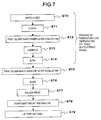
- a furnace temperature was raised from a room temperature to approximately 500°c at a temperature raising rate of 100°c/h and was maintained this temperature for two hours, and furthermore, was raised to a maximum temperature of approximately 890°c at a temperature raising rate of 100°c/h and was maintained the temperature for two hours (S50).
- a conductor pattern to be a wiring layer of a thick film ceramic board was screen printed with a conductor paste over the surface of each glass ceramic board thus fabricated (S51).
- the conductor paste to be used was obtained which has an appropriate viscosity by adding a proper amount of organic vehicle (polysaccharides such as cellulose) and an organic solvent (terpineol or the like) to conductor powder containing 1 wt% of platinum powder or palladium powder and 99 wt% of a silver particle which have a specific surface area of 0.3 m 2 /g to 3.0 m 2 /g. As a matter of course, no glass was contained.
- the conductor pattern of the surface of each glass ceramic board was fired in the air at a temperature of ⁇ 50°c of the softening point of the borosilicate glass contained in the glass ceramic board (S52).
- a wiring layer was thus formed, it was coated with a glass paste having a low dielectric constant (S53) and the glass paste was fired. Consequently, an insulating layer was formed on the wiring layer (S54).
- a conductor pattern to be a component-mounting pad and a terminal pad was screen printed on the surface of the uppermost insulating layer of each glass ceramic board through a conductor paste having the same composition as that of the conductor paste used in the formation of the wiring layer (S55).
- the conductor pattern was fired at a temperature of ⁇ 50°c of the softening point of the borosilicate glass contained in the glass ceramic board. Consequently, the component-mounting pad and the terminal pad were formed (S56). Consequently, a thick film ceramic board was completed,
- each solder paste was heated to approximately 240°c in a reflow furnace to be subjected to reflow in such a state that the LSI-mounting surface was in contact with the solder paste. Consequently, the LSI was mounted on each thick film ceramic board (S58).
- a green sheet of glass ceramic was first fabricated by the same process as that in the above case utilizing the thick film processing (S70).
- the green sheet was divided into green sheet pieces having a proper size and a through hole for connecting upper and lower wiring layers was punched out of each green sheet piece through a mold (S71).
- printing was carried out on each green sheet piece so that the through hole of the green sheet piece was filled with the conductor paste and a wiring pattern was printed on the surface of the green sheet piece.
- conductor patterns to be a component-mounting pad and a terminal pad were collectively formed on the surface of the green sheet piece to be the uppermost layer of a low temperature sintered glass ceramic multilayered board (S72).
- each solder paste was heated to approximately 240°c in a reflow furnace to be subjected to reflow in such a state that the LSI-mounting surface was in contact with the solder paste. Consequently, the LSI is mounted on each low temperature fired glass ceramic multilayered board (S78).
- the bonding pad of the ceramic multilayered board can also be formed of the same silver-based conductor as that of the wiring pattern. Therefore, the surface layer conductor of the ceramic multilayered board can be formed through one-time printing and one-time firing. Consequently, a production cost can be reduced usefully.
Landscapes
- Chemical & Material Sciences (AREA)
- Dispersion Chemistry (AREA)
- Engineering & Computer Science (AREA)
- Microelectronics & Electronic Packaging (AREA)
- Parts Printed On Printed Circuit Boards (AREA)
- Conductive Materials (AREA)
- Manufacturing Of Printed Wiring (AREA)
- Wire Bonding (AREA)
- Non-Insulated Conductors (AREA)
Applications Claiming Priority (2)
| Application Number | Priority Date | Filing Date | Title |
|---|---|---|---|
| JP2001174690 | 2001-06-08 | ||
| JP2001174690A JP2002362987A (ja) | 2001-06-08 | 2001-06-08 | 電子部品およびその製造方法 |
Publications (2)
| Publication Number | Publication Date |
|---|---|
| EP1265464A2 true EP1265464A2 (de) | 2002-12-11 |
| EP1265464A3 EP1265464A3 (de) | 2005-09-07 |
Family
ID=19015940
Family Applications (1)
| Application Number | Title | Priority Date | Filing Date |
|---|---|---|---|
| EP01307405A Withdrawn EP1265464A3 (de) | 2001-06-08 | 2001-08-31 | Elektronisches Bauteil und Verfahren zu dessen Herstellung |
Country Status (3)
| Country | Link |
|---|---|
| US (1) | US6815073B2 (de) |
| EP (1) | EP1265464A3 (de) |
| JP (1) | JP2002362987A (de) |
Cited By (1)
| Publication number | Priority date | Publication date | Assignee | Title |
|---|---|---|---|---|
| US10560691B2 (en) * | 2017-12-22 | 2020-02-11 | CI Tech Sensors, AG | System, having a processing device and a camera connected thereto. for the detection of a machine-readable security feature of a value document and method for exchanging a camera of such a system |
Families Citing this family (6)
| Publication number | Priority date | Publication date | Assignee | Title |
|---|---|---|---|---|
| JP2007235082A (ja) * | 2006-02-02 | 2007-09-13 | E I Du Pont De Nemours & Co | 太陽電池電極用ペースト |
| US8555491B2 (en) | 2007-07-19 | 2013-10-15 | Alpha Metals, Inc. | Methods of attaching a die to a substrate |
| WO2013191288A1 (ja) * | 2012-06-21 | 2013-12-27 | 京セラ株式会社 | 回路基板およびこれを備える電子装置 |
| JP6040729B2 (ja) * | 2012-11-26 | 2016-12-07 | 三菱マテリアル株式会社 | 半導体装置及び半導体装置の製造方法 |
| JP6613929B2 (ja) * | 2016-02-01 | 2019-12-04 | 三菱マテリアル株式会社 | Ag下地層付き金属部材、Ag下地層付き絶縁回路基板、半導体装置、ヒートシンク付き絶縁回路基板、及び、Ag下地層付き金属部材の製造方法 |
| WO2019064738A1 (ja) * | 2017-09-29 | 2019-04-04 | 株式会社村田製作所 | 導電性ペースト、ガラス物品、及びガラス物品の製造方法 |
Family Cites Families (13)
| Publication number | Priority date | Publication date | Assignee | Title |
|---|---|---|---|---|
| US3872360A (en) * | 1973-01-08 | 1975-03-18 | Du Pont | Capacitors with nickel containing electrodes |
| US3929491A (en) * | 1974-01-24 | 1975-12-30 | Electro Oxide Corp | Bonded silver article, composition, and method of bonding silver to a ceramic substrate |
| US4001146A (en) * | 1975-02-26 | 1977-01-04 | E. I. Du Pont De Nemours And Company | Novel silver compositions |
| JPS53147968A (en) * | 1977-05-30 | 1978-12-23 | Hitachi Ltd | Thick film circuit board |
| US4636332A (en) * | 1985-11-01 | 1987-01-13 | E. I. Du Pont De Nemours And Company | Thick film conductor composition |
| JP2701864B2 (ja) | 1988-05-24 | 1998-01-21 | 株式会社デンソー | 導体組成物およびそれより成る導体を有したセラミック基板 |
| JP3223199B2 (ja) * | 1991-10-25 | 2001-10-29 | ティーディーケイ株式会社 | 多層セラミック部品の製造方法および多層セラミック部品 |
| US5527627A (en) * | 1993-03-29 | 1996-06-18 | Delco Electronics Corp. | Ink composition for an ultra-thick thick film for thermal management of a hybrid circuit |
| US5292359A (en) * | 1993-07-16 | 1994-03-08 | Industrial Technology Research Institute | Process for preparing silver-palladium powders |
| EP0651602B1 (de) * | 1993-10-29 | 1999-04-07 | Matsushita Electric Industrial Co., Ltd. | Leitfähige Pastenzusammensetzung zum Füllen von Kontaktlöchern, Leiterplatte unter Anwendung dieser leifähigen Paste und Verfahren zur Herstellung |
| JPH08162762A (ja) * | 1994-12-02 | 1996-06-21 | Sumitomo Metal Mining Co Ltd | ガラスセラミック多層回路基板 |
| US6338893B1 (en) * | 1998-10-28 | 2002-01-15 | Ngk Spark Plug Co., Ltd. | Conductive paste and ceramic printed circuit substrate using the same |
| JP2001052930A (ja) * | 1999-08-06 | 2001-02-23 | Tdk Corp | 積層インダクタとその製造方法 |
-
2001
- 2001-06-08 JP JP2001174690A patent/JP2002362987A/ja active Pending
- 2001-08-30 US US09/941,988 patent/US6815073B2/en not_active Expired - Fee Related
- 2001-08-31 EP EP01307405A patent/EP1265464A3/de not_active Withdrawn
Cited By (1)
| Publication number | Priority date | Publication date | Assignee | Title |
|---|---|---|---|---|
| US10560691B2 (en) * | 2017-12-22 | 2020-02-11 | CI Tech Sensors, AG | System, having a processing device and a camera connected thereto. for the detection of a machine-readable security feature of a value document and method for exchanging a camera of such a system |
Also Published As
| Publication number | Publication date |
|---|---|
| JP2002362987A (ja) | 2002-12-18 |
| US20020197488A1 (en) | 2002-12-26 |
| EP1265464A3 (de) | 2005-09-07 |
| US6815073B2 (en) | 2004-11-09 |
Similar Documents
| Publication | Publication Date | Title |
|---|---|---|
| KR20010049529A (ko) | 세라믹 기판의 제조방법 및 소성되지 않은 세라믹 기판 | |
| WO2007032167A1 (ja) | セラミック多層基板およびその製造方法 | |
| JP3826685B2 (ja) | ガラスセラミック回路基板の製造方法 | |
| JP2001307547A (ja) | 導電性組成物およびそれを用いた印刷回路板 | |
| US6815073B2 (en) | Electronic component and method of manufacturing the same | |
| JP3517062B2 (ja) | 銅メタライズ組成物及びそれを用いたガラスセラミック配線基板 | |
| JP2004047856A (ja) | 導体ペースト及び印刷方法並びにセラミック多層回路基板の製造方法 | |
| JP3347578B2 (ja) | 配線基板 | |
| JPH09221375A (ja) | セラミックス基板及びその製造方法 | |
| JP3785903B2 (ja) | 多層基板及びその製造方法 | |
| JP2002043758A (ja) | 多層基板及びその製造方法 | |
| JPH11284296A (ja) | 配線基板 | |
| JPH1116418A (ja) | 銅メタライズ組成物及びそれを用いたガラスセラミック配線基板 | |
| JP3666308B2 (ja) | 導電性ペーストおよびセラミック電子部品 | |
| JP2011029534A (ja) | 多層配線基板 | |
| JP4646362B2 (ja) | 導体組成物およびこれを用いた配線基板 | |
| JP2006100448A (ja) | 電子部品の製造方法 | |
| JPH11186727A (ja) | 配線基板およびその製造方法 | |
| JP3643264B2 (ja) | 導体ペーストおよびこれを用いた配線基板 | |
| JP3905991B2 (ja) | ガラスセラミック配線基板 | |
| JP5313526B2 (ja) | 低温焼成多層基板用導電性ペースト | |
| JPH1153940A (ja) | 銅メタライズ組成物及びそれを用いたガラスセラミック配線基板 | |
| JP3652184B2 (ja) | 導体ペースト、ガラスセラミック配線基板並びにその製法 | |
| JP3252743B2 (ja) | セラミックス回路基板 | |
| JP4610185B2 (ja) | 配線基板並びにその製造方法 |
Legal Events
| Date | Code | Title | Description |
|---|---|---|---|
| PUAI | Public reference made under article 153(3) epc to a published international application that has entered the european phase |
Free format text: ORIGINAL CODE: 0009012 |
|
| 17P | Request for examination filed |
Effective date: 20010919 |
|
| AK | Designated contracting states |
Kind code of ref document: A2 Designated state(s): AT BE CH CY DE DK ES FI FR GB GR IE IT LI LU MC NL PT SE TR |
|
| AX | Request for extension of the european patent |
Free format text: AL;LT;LV;MK;RO;SI |
|
| PUAL | Search report despatched |
Free format text: ORIGINAL CODE: 0009013 |
|
| AK | Designated contracting states |
Kind code of ref document: A3 Designated state(s): AT BE CH CY DE DK ES FI FR GB GR IE IT LI LU MC NL PT SE TR |
|
| AX | Request for extension of the european patent |
Extension state: AL LT LV MK RO SI |
|
| AKX | Designation fees paid |
Designated state(s): DE FR GB IT |
|
| STAA | Information on the status of an ep patent application or granted ep patent |
Free format text: STATUS: THE APPLICATION HAS BEEN WITHDRAWN |
|
| 18W | Application withdrawn |
Effective date: 20080320 |