EP1263136B1 - Structures de filtres pour interfaces de circuits intégrés - Google Patents
Structures de filtres pour interfaces de circuits intégrés Download PDFInfo
- Publication number
- EP1263136B1 EP1263136B1 EP02010250A EP02010250A EP1263136B1 EP 1263136 B1 EP1263136 B1 EP 1263136B1 EP 02010250 A EP02010250 A EP 02010250A EP 02010250 A EP02010250 A EP 02010250A EP 1263136 B1 EP1263136 B1 EP 1263136B1
- Authority
- EP
- European Patent Office
- Prior art keywords
- interconnect system
- pcb
- frequency response
- bond pad
- conductive path
- Prior art date
- Legal status (The legal status is an assumption and is not a legal conclusion. Google has not performed a legal analysis and makes no representation as to the accuracy of the status listed.)
- Expired - Lifetime
Links
Images
Classifications
-
- H—ELECTRICITY
- H05—ELECTRIC TECHNIQUES NOT OTHERWISE PROVIDED FOR
- H05K—PRINTED CIRCUITS; CASINGS OR CONSTRUCTIONAL DETAILS OF ELECTRIC APPARATUS; MANUFACTURE OF ASSEMBLAGES OF ELECTRICAL COMPONENTS
- H05K1/00—Printed circuits
- H05K1/02—Details
- H05K1/0213—Electrical arrangements not otherwise provided for
- H05K1/0237—High frequency adaptations
- H05K1/025—Impedance arrangements, e.g. impedance matching, reduction of parasitic impedance
-
- H—ELECTRICITY
- H03—ELECTRONIC CIRCUITRY
- H03H—IMPEDANCE NETWORKS, e.g. RESONANT CIRCUITS; RESONATORS
- H03H7/00—Multiple-port networks comprising only passive electrical elements as network components
- H03H7/01—Frequency selective two-port networks
- H03H7/0115—Frequency selective two-port networks comprising only inductors and capacitors
-
- H—ELECTRICITY
- H03—ELECTRONIC CIRCUITRY
- H03H—IMPEDANCE NETWORKS, e.g. RESONANT CIRCUITS; RESONATORS
- H03H7/00—Multiple-port networks comprising only passive electrical elements as network components
- H03H7/38—Impedance-matching networks
-
- H—ELECTRICITY
- H05—ELECTRIC TECHNIQUES NOT OTHERWISE PROVIDED FOR
- H05K—PRINTED CIRCUITS; CASINGS OR CONSTRUCTIONAL DETAILS OF ELECTRIC APPARATUS; MANUFACTURE OF ASSEMBLAGES OF ELECTRICAL COMPONENTS
- H05K1/00—Printed circuits
- H05K1/02—Details
- H05K1/0213—Electrical arrangements not otherwise provided for
- H05K1/0216—Reduction of cross-talk, noise or electromagnetic interference
- H05K1/023—Reduction of cross-talk, noise or electromagnetic interference using auxiliary mounted passive components or auxiliary substances
- H05K1/0233—Filters, inductors or a magnetic substance
-
- H—ELECTRICITY
- H05—ELECTRIC TECHNIQUES NOT OTHERWISE PROVIDED FOR
- H05K—PRINTED CIRCUITS; CASINGS OR CONSTRUCTIONAL DETAILS OF ELECTRIC APPARATUS; MANUFACTURE OF ASSEMBLAGES OF ELECTRICAL COMPONENTS
- H05K1/00—Printed circuits
- H05K1/02—Details
- H05K1/11—Printed elements for providing electric connections to or between printed circuits
- H05K1/115—Via connections; Lands around holes or via connections
- H05K1/116—Lands, clearance holes or other lay-out details concerning the surrounding of a via
-
- H—ELECTRICITY
- H05—ELECTRIC TECHNIQUES NOT OTHERWISE PROVIDED FOR
- H05K—PRINTED CIRCUITS; CASINGS OR CONSTRUCTIONAL DETAILS OF ELECTRIC APPARATUS; MANUFACTURE OF ASSEMBLAGES OF ELECTRICAL COMPONENTS
- H05K1/00—Printed circuits
- H05K1/16—Printed circuits incorporating printed electric components, e.g. printed resistor, capacitor, inductor
- H05K1/162—Printed circuits incorporating printed electric components, e.g. printed resistor, capacitor, inductor incorporating printed capacitors
-
- H—ELECTRICITY
- H01—ELECTRIC ELEMENTS
- H01L—SEMICONDUCTOR DEVICES NOT COVERED BY CLASS H10
- H01L2224/00—Indexing scheme for arrangements for connecting or disconnecting semiconductor or solid-state bodies and methods related thereto as covered by H01L24/00
- H01L2224/01—Means for bonding being attached to, or being formed on, the surface to be connected, e.g. chip-to-package, die-attach, "first-level" interconnects; Manufacturing methods related thereto
- H01L2224/42—Wire connectors; Manufacturing methods related thereto
- H01L2224/47—Structure, shape, material or disposition of the wire connectors after the connecting process
- H01L2224/48—Structure, shape, material or disposition of the wire connectors after the connecting process of an individual wire connector
- H01L2224/4805—Shape
- H01L2224/4809—Loop shape
- H01L2224/48091—Arched
-
- H—ELECTRICITY
- H01—ELECTRIC ELEMENTS
- H01L—SEMICONDUCTOR DEVICES NOT COVERED BY CLASS H10
- H01L2924/00—Indexing scheme for arrangements or methods for connecting or disconnecting semiconductor or solid-state bodies as covered by H01L24/00
- H01L2924/30—Technical effects
- H01L2924/301—Electrical effects
- H01L2924/30107—Inductance
-
- H—ELECTRICITY
- H01—ELECTRIC ELEMENTS
- H01L—SEMICONDUCTOR DEVICES NOT COVERED BY CLASS H10
- H01L2924/00—Indexing scheme for arrangements or methods for connecting or disconnecting semiconductor or solid-state bodies as covered by H01L24/00
- H01L2924/30—Technical effects
- H01L2924/301—Electrical effects
- H01L2924/3011—Impedance
-
- H—ELECTRICITY
- H03—ELECTRONIC CIRCUITRY
- H03H—IMPEDANCE NETWORKS, e.g. RESONANT CIRCUITS; RESONATORS
- H03H1/00—Constructional details of impedance networks whose electrical mode of operation is not specified or applicable to more than one type of network
- H03H2001/0021—Constructional details
- H03H2001/0085—Multilayer, e.g. LTCC, HTCC, green sheets
-
- H—ELECTRICITY
- H05—ELECTRIC TECHNIQUES NOT OTHERWISE PROVIDED FOR
- H05K—PRINTED CIRCUITS; CASINGS OR CONSTRUCTIONAL DETAILS OF ELECTRIC APPARATUS; MANUFACTURE OF ASSEMBLAGES OF ELECTRICAL COMPONENTS
- H05K1/00—Printed circuits
- H05K1/02—Details
- H05K1/0213—Electrical arrangements not otherwise provided for
- H05K1/0216—Reduction of cross-talk, noise or electromagnetic interference
- H05K1/023—Reduction of cross-talk, noise or electromagnetic interference using auxiliary mounted passive components or auxiliary substances
- H05K1/0231—Capacitors or dielectric substances
-
- H—ELECTRICITY
- H05—ELECTRIC TECHNIQUES NOT OTHERWISE PROVIDED FOR
- H05K—PRINTED CIRCUITS; CASINGS OR CONSTRUCTIONAL DETAILS OF ELECTRIC APPARATUS; MANUFACTURE OF ASSEMBLAGES OF ELECTRICAL COMPONENTS
- H05K1/00—Printed circuits
- H05K1/02—Details
- H05K1/11—Printed elements for providing electric connections to or between printed circuits
- H05K1/111—Pads for surface mounting, e.g. lay-out
- H05K1/112—Pads for surface mounting, e.g. lay-out directly combined with via connections
- H05K1/113—Via provided in pad; Pad over filled via
-
- H—ELECTRICITY
- H05—ELECTRIC TECHNIQUES NOT OTHERWISE PROVIDED FOR
- H05K—PRINTED CIRCUITS; CASINGS OR CONSTRUCTIONAL DETAILS OF ELECTRIC APPARATUS; MANUFACTURE OF ASSEMBLAGES OF ELECTRICAL COMPONENTS
- H05K2201/00—Indexing scheme relating to printed circuits covered by H05K1/00
- H05K2201/09—Shape and layout
- H05K2201/09209—Shape and layout details of conductors
- H05K2201/09218—Conductive traces
- H05K2201/09263—Meander
-
- H—ELECTRICITY
- H05—ELECTRIC TECHNIQUES NOT OTHERWISE PROVIDED FOR
- H05K—PRINTED CIRCUITS; CASINGS OR CONSTRUCTIONAL DETAILS OF ELECTRIC APPARATUS; MANUFACTURE OF ASSEMBLAGES OF ELECTRICAL COMPONENTS
- H05K2201/00—Indexing scheme relating to printed circuits covered by H05K1/00
- H05K2201/09—Shape and layout
- H05K2201/09209—Shape and layout details of conductors
- H05K2201/09372—Pads and lands
- H05K2201/09454—Inner lands, i.e. lands around via or plated through-hole in internal layer of multilayer PCB
-
- H—ELECTRICITY
- H05—ELECTRIC TECHNIQUES NOT OTHERWISE PROVIDED FOR
- H05K—PRINTED CIRCUITS; CASINGS OR CONSTRUCTIONAL DETAILS OF ELECTRIC APPARATUS; MANUFACTURE OF ASSEMBLAGES OF ELECTRICAL COMPONENTS
- H05K2201/00—Indexing scheme relating to printed circuits covered by H05K1/00
- H05K2201/09—Shape and layout
- H05K2201/09209—Shape and layout details of conductors
- H05K2201/09654—Shape and layout details of conductors covering at least two types of conductors provided for in H05K2201/09218 - H05K2201/095
- H05K2201/09672—Superposed layout, i.e. in different planes
-
- H—ELECTRICITY
- H05—ELECTRIC TECHNIQUES NOT OTHERWISE PROVIDED FOR
- H05K—PRINTED CIRCUITS; CASINGS OR CONSTRUCTIONAL DETAILS OF ELECTRIC APPARATUS; MANUFACTURE OF ASSEMBLAGES OF ELECTRICAL COMPONENTS
- H05K2201/00—Indexing scheme relating to printed circuits covered by H05K1/00
- H05K2201/09—Shape and layout
- H05K2201/09209—Shape and layout details of conductors
- H05K2201/09654—Shape and layout details of conductors covering at least two types of conductors provided for in H05K2201/09218 - H05K2201/095
- H05K2201/09727—Varying width along a single conductor; Conductors or pads having different widths
-
- H—ELECTRICITY
- H05—ELECTRIC TECHNIQUES NOT OTHERWISE PROVIDED FOR
- H05K—PRINTED CIRCUITS; CASINGS OR CONSTRUCTIONAL DETAILS OF ELECTRIC APPARATUS; MANUFACTURE OF ASSEMBLAGES OF ELECTRICAL COMPONENTS
- H05K2201/00—Indexing scheme relating to printed circuits covered by H05K1/00
- H05K2201/10—Details of components or other objects attached to or integrated in a printed circuit board
- H05K2201/10613—Details of electrical connections of non-printed components, e.g. special leads
- H05K2201/10621—Components characterised by their electrical contacts
- H05K2201/10689—Leaded Integrated Circuit [IC] package, e.g. dual-in-line [DIL]
-
- H—ELECTRICITY
- H05—ELECTRIC TECHNIQUES NOT OTHERWISE PROVIDED FOR
- H05K—PRINTED CIRCUITS; CASINGS OR CONSTRUCTIONAL DETAILS OF ELECTRIC APPARATUS; MANUFACTURE OF ASSEMBLAGES OF ELECTRICAL COMPONENTS
- H05K3/00—Apparatus or processes for manufacturing printed circuits
- H05K3/30—Assembling printed circuits with electric components, e.g. with resistor
- H05K3/32—Assembling printed circuits with electric components, e.g. with resistor electrically connecting electric components or wires to printed circuits
- H05K3/34—Assembling printed circuits with electric components, e.g. with resistor electrically connecting electric components or wires to printed circuits by soldering
- H05K3/341—Surface mounted components
- H05K3/3421—Leaded components
-
- H—ELECTRICITY
- H05—ELECTRIC TECHNIQUES NOT OTHERWISE PROVIDED FOR
- H05K—PRINTED CIRCUITS; CASINGS OR CONSTRUCTIONAL DETAILS OF ELECTRIC APPARATUS; MANUFACTURE OF ASSEMBLAGES OF ELECTRICAL COMPONENTS
- H05K3/00—Apparatus or processes for manufacturing printed circuits
- H05K3/40—Forming printed elements for providing electric connections to or between printed circuits
- H05K3/42—Plated through-holes or plated via connections
- H05K3/429—Plated through-holes specially for multilayer circuits, e.g. having connections to inner circuit layers
Definitions
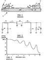
- FIG. 1 is a simplified sectional elevation view of the prior art interconnect system, including a printed circuit board (PCB) 10 upon which is mounted a pair of integrated circuits (ICs) 12 and 14.
- IC 12 includes an integrated circuit chip 16 contained within an IC package 18.
- a bond pad 20 on the surface of chip 16 acts as an input/output (I/O) terminal for signals entering and/or departing chip 16.
- a typical IC will include several bond pads, but for simplicity only one is shown in FIG. 1 .
- a bond wire 22 links bond pad 20 to a conductive leg 24 extending outward from package 18.
- the circuit formed by capacitors C1, C2, inductors L1 and L2, resistors R1 and R2, and impedance Z0 has a reactive impedance that can substantially attenuate and distort signals passing between driver 40 and receiver 42.
- the conventional approach to reducing the amount of signal distortion and attenuation in high frequency applications has been to minimize bond wire inductances L1 and L2 and capacitances C1 and C2.
- Inductances L1 and L2 are minimized by keeping bond wires 20, 27 and package legs 24, 29 as small as possible.
- Capacitances C1 and C2 are minimized by keeping bond pads 20 and 28 as small as possible.
- FIG. 3 illustrates the frequency response characteristics of the prior art interconnect system of FIGs. 1 and 2 when components are set to the values indicated in Table I.
- the desired frequency response characteristics for an interconnect system depends on its application. For example, when the interconnect system is to convey an analog signal with little distortion or noise, it is usually desirable that the passband be only as wide as needed to pass the highest frequency signal expected, that the passband be as flat as possible to avoid signal distortion, and that all areas of the stopband have maximal attenuation so as to block high frequency noise.
- the interconnect system of FIG. 2 to convey an analog signal having components up to 3GHz. We first note that the passband (approximately 2GHz) is not wide enough for the application.
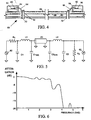
- FIG. 5 is an equivalent circuit diagram of the interconnect system of FIG. 4 in accordance with the invention.
- a driver 80 within IC 54 is connected to pad 52 through impedance R 1 and a receiver having input impedance R 2 within IC 58 connected to pad 56.
- Bond wire 60 and package leg 64 are modeled as inductance L1 while bond wire 62 and package leg 66 are modeled as inductance L2.
- the capacitances of pads 52 and 56 appear in FIG. 5 as capacitors C1 and C2 and the impedance of PCB trace 68 appears as its characteristic impedance Z0. Since vias 60 and 72 are primarily capacitive, their capacitances appear in FIG. 5 as capacitors C1 VIA and C2 VIA .
Claims (5)
- Procédé destiné à optimiser sensiblement une caractéristique d'une réponse en fréquence d'un système d'interconnexion connectant un premier et un second circuit imprimé (IC) (54, 58) monté sur une carte à circuit imprimé (PCB) (50) ayant une piste PCB (68), le système d'interconnexion comprenant :- un premier plot de connexion (52) sur ledit IC (54), une première ligne conductrice (60, 64) reliant ledit premier plot de connexion (52) à ladite piste de la carte PCB (68) et formant une première inductance (L1) et- un second plot de connexion (56) sur ledit second IC (56), une seconde ligne conductrice (62, 66) reliant ledit second plot de connexion (56) à ladite piste de carte PCB (68) et formant une seconde inductance (L2),
le procédé comprenant les étapes consistant à :additionner les capacités (C1VIA, C2VIA) à ladite piste PCB (68), les capacités additionnées (C1VIA, C2VIA) étant ajustées par rapport à l'impédance des autres composants du système d'interconnexion ; et/ouaugmenter lesdites première et/ou seconde inductances (L1, L2) au-dessus de leurs niveaux minimum, la grandeur de la première et seconde inductance (L1, L2) étant augmentées en augmentant la longueur de la première ligne de conduction (60, 64), en augmentant la longueur de la seconde ligne de conduction (62, 66) ou en ajoutant des éléments inductifs en série avec des circuits de voies (60, 62) faisant partie de la première et seconde lignes conductrices. - Procédé selon la revendication 1, dans lequel ladite caractéristique de réponse en fréquence est l'une d'une largeur de bande passante maximale, d'une planéité de bande passante maximale et d'une puissance de bande passante maximale.
- Procédé selon la revendication 1, dans lequel ladite première inductance ajoutée à ladite première ligne conductrice est dimensionnée de sorte que ledit système d'interconnexion agit sensiblement comme un filtre de Butterworth à pôles multiples.
- Procédé selon la revendication 1, dans lequel ladite première inductance ajoutée à ladite première ligne conductrice est dimensionnée de sorte que ledit système d'interconnexion agit sensiblement en tant que filtre Tchebychev à pôles multiples.
- Procédé selon la revendication 1, dans lequel le système d'interconnexion interconnecte un circuit d'attaque (80) sur le premier circuit intégré IC (54) à un récepteur (82) sur un second circuit intégré IC (58), dans lequel ledit premier plot de connexion (52) mis en oeuvre sur ledit premier circuit intégré IC est relié audit circuit d'attaque.
Applications Claiming Priority (3)
| Application Number | Priority Date | Filing Date | Title |
|---|---|---|---|
| US258184 | 1999-02-25 | ||
| US09/258,184 US6208225B1 (en) | 1999-02-25 | 1999-02-25 | Filter structures for integrated circuit interfaces |
| EP00908800A EP1157459B1 (fr) | 1999-02-25 | 2000-02-23 | Structures filtres pour interfaces de circuits integres |
Related Parent Applications (1)
| Application Number | Title | Priority Date | Filing Date |
|---|---|---|---|
| EP00908800A Division EP1157459B1 (fr) | 1999-02-25 | 2000-02-23 | Structures filtres pour interfaces de circuits integres |
Publications (3)
| Publication Number | Publication Date |
|---|---|
| EP1263136A2 EP1263136A2 (fr) | 2002-12-04 |
| EP1263136A3 EP1263136A3 (fr) | 2003-05-07 |
| EP1263136B1 true EP1263136B1 (fr) | 2008-10-15 |
Family
ID=22979461
Family Applications (2)
| Application Number | Title | Priority Date | Filing Date |
|---|---|---|---|
| EP00908800A Expired - Lifetime EP1157459B1 (fr) | 1999-02-25 | 2000-02-23 | Structures filtres pour interfaces de circuits integres |
| EP02010250A Expired - Lifetime EP1263136B1 (fr) | 1999-02-25 | 2000-02-23 | Structures de filtres pour interfaces de circuits intégrés |
Family Applications Before (1)
| Application Number | Title | Priority Date | Filing Date |
|---|---|---|---|
| EP00908800A Expired - Lifetime EP1157459B1 (fr) | 1999-02-25 | 2000-02-23 | Structures filtres pour interfaces de circuits integres |
Country Status (8)
| Country | Link |
|---|---|
| US (2) | US6208225B1 (fr) |
| EP (2) | EP1157459B1 (fr) |
| JP (2) | JP2002538609A (fr) |
| KR (1) | KR100638755B1 (fr) |
| AU (1) | AU3007700A (fr) |
| DE (2) | DE60000863T2 (fr) |
| TW (1) | TWI228965B (fr) |
| WO (1) | WO2000051232A1 (fr) |
Families Citing this family (87)
| Publication number | Priority date | Publication date | Assignee | Title |
|---|---|---|---|---|
| US5729150A (en) * | 1995-12-01 | 1998-03-17 | Cascade Microtech, Inc. | Low-current probe card with reduced triboelectric current generating cables |
| US5914613A (en) * | 1996-08-08 | 1999-06-22 | Cascade Microtech, Inc. | Membrane probing system with local contact scrub |
| US7321485B2 (en) | 1997-04-08 | 2008-01-22 | X2Y Attenuators, Llc | Arrangement for energy conditioning |
| US9054094B2 (en) | 1997-04-08 | 2015-06-09 | X2Y Attenuators, Llc | Energy conditioning circuit arrangement for integrated circuit |
| US6018448A (en) * | 1997-04-08 | 2000-01-25 | X2Y Attenuators, L.L.C. | Paired multi-layered dielectric independent passive component architecture resulting in differential and common mode filtering with surge protection in one integrated package |
| US7336468B2 (en) | 1997-04-08 | 2008-02-26 | X2Y Attenuators, Llc | Arrangement for energy conditioning |
| US7301748B2 (en) | 1997-04-08 | 2007-11-27 | Anthony Anthony A | Universal energy conditioning interposer with circuit architecture |
| US6034533A (en) * | 1997-06-10 | 2000-03-07 | Tervo; Paul A. | Low-current pogo probe card |
| US6256882B1 (en) * | 1998-07-14 | 2001-07-10 | Cascade Microtech, Inc. | Membrane probing system |
| US6218910B1 (en) * | 1999-02-25 | 2001-04-17 | Formfactor, Inc. | High bandwidth passive integrated circuit tester probe card assembly |
| US6538538B2 (en) | 1999-02-25 | 2003-03-25 | Formfactor, Inc. | High frequency printed circuit board via |
| US6578264B1 (en) * | 1999-06-04 | 2003-06-17 | Cascade Microtech, Inc. | Method for constructing a membrane probe using a depression |
| JP2001202400A (ja) * | 2000-01-21 | 2001-07-27 | Nec Corp | 電源デカップリング回路生成システム及び電源デカップリング回路生成方法 |
| US6838890B2 (en) * | 2000-02-25 | 2005-01-04 | Cascade Microtech, Inc. | Membrane probing system |
| US6646521B1 (en) * | 2000-09-15 | 2003-11-11 | Hei, Inc. | Connection for conducting high frequency signal between a circuit and a discrete electric component |
| CA2425946A1 (fr) * | 2000-10-17 | 2002-04-25 | X2Y Attenuators, Llc | Amalgame de protection et chemins d'energie proteges et autres elements pour circuit(s) ou unique ou multiples dote(s) d'un noeud de reference commun |
| DE10143173A1 (de) | 2000-12-04 | 2002-06-06 | Cascade Microtech Inc | Wafersonde |
| US6617943B1 (en) | 2001-07-27 | 2003-09-09 | Applied Micro Circuits Corporation | Package substrate interconnect layout for providing bandpass/lowpass filtering |
| WO2003052435A1 (fr) | 2001-08-21 | 2003-06-26 | Cascade Microtech, Inc. | Systeme de detection a membrane |
| US6816031B1 (en) | 2001-12-04 | 2004-11-09 | Formfactor, Inc. | Adjustable delay transmission line |
| US20060006888A1 (en) * | 2003-02-04 | 2006-01-12 | Microfabrica Inc. | Electrochemically fabricated microprobes |
| US7412767B2 (en) * | 2003-02-04 | 2008-08-19 | Microfabrica, Inc. | Microprobe tips and methods for making |
| US7363705B2 (en) * | 2003-02-04 | 2008-04-29 | Microfabrica, Inc. | Method of making a contact |
| US20050184748A1 (en) * | 2003-02-04 | 2005-08-25 | Microfabrica Inc. | Pin-type probes for contacting electronic circuits and methods for making such probes |
| US20050104609A1 (en) * | 2003-02-04 | 2005-05-19 | Microfabrica Inc. | Microprobe tips and methods for making |
| US7640651B2 (en) * | 2003-12-31 | 2010-01-05 | Microfabrica Inc. | Fabrication process for co-fabricating multilayer probe array and a space transformer |
| US7531077B2 (en) | 2003-02-04 | 2009-05-12 | Microfabrica Inc. | Electrochemical fabrication process for forming multilayer multimaterial microprobe structures |
| US7273812B2 (en) * | 2002-05-07 | 2007-09-25 | Microfabrica Inc. | Microprobe tips and methods for making |
| US20060238209A1 (en) * | 2002-05-07 | 2006-10-26 | Microfabrica Inc. | Vertical microprobes for contacting electronic components and method for making such probes |
| US20060053625A1 (en) * | 2002-05-07 | 2006-03-16 | Microfabrica Inc. | Microprobe tips and methods for making |
| US20060051948A1 (en) * | 2003-02-04 | 2006-03-09 | Microfabrica Inc. | Microprobe tips and methods for making |
| US7265565B2 (en) * | 2003-02-04 | 2007-09-04 | Microfabrica Inc. | Cantilever microprobes for contacting electronic components and methods for making such probes |
| US6724205B1 (en) * | 2002-11-13 | 2004-04-20 | Cascade Microtech, Inc. | Probe for combined signals |
| US7002220B1 (en) | 2003-01-29 | 2006-02-21 | Marvell International Ltd. | ESD protection circuit |
| US6911739B1 (en) | 2003-01-29 | 2005-06-28 | Marvell International Ltd. | Methods and apparatus for improving high frequency input/output performance |
| US7180718B2 (en) * | 2003-01-31 | 2007-02-20 | X2Y Attenuators, Llc | Shielded energy conditioner |
| US7567089B2 (en) * | 2003-02-04 | 2009-07-28 | Microfabrica Inc. | Two-part microprobes for contacting electronic components and methods for making such probes |
| US20080211524A1 (en) * | 2003-02-04 | 2008-09-04 | Microfabrica Inc. | Electrochemically Fabricated Microprobes |
| US8613846B2 (en) * | 2003-02-04 | 2013-12-24 | Microfabrica Inc. | Multi-layer, multi-material fabrication methods for producing micro-scale and millimeter-scale devices with enhanced electrical and/or mechanical properties |
| US10416192B2 (en) | 2003-02-04 | 2019-09-17 | Microfabrica Inc. | Cantilever microprobes for contacting electronic components |
| US9244101B2 (en) * | 2003-02-04 | 2016-01-26 | University Of Southern California | Electrochemical fabrication process for forming multilayer multimaterial microprobe structures |
| US20080157793A1 (en) * | 2003-02-04 | 2008-07-03 | Microfabrica Inc. | Vertical Microprobes for Contacting Electronic Components and Method for Making Such Probes |
| EP1471575A1 (fr) * | 2003-04-24 | 2004-10-27 | Samsung Electronics Co., Ltd. | Support à puce rf avec un composant inductif intégré et procédé pour sa fabrication |
| US9671429B2 (en) | 2003-05-07 | 2017-06-06 | University Of Southern California | Multi-layer, multi-material micro-scale and millimeter-scale devices with enhanced electrical and/or mechanical properties |
| US7414505B2 (en) | 2003-05-13 | 2008-08-19 | Samsung Electronics Co., Ltd. | High frequency inductor having low inductance and low inductance variation and method of manufacturing the same |
| US7057404B2 (en) | 2003-05-23 | 2006-06-06 | Sharp Laboratories Of America, Inc. | Shielded probe for testing a device under test |
| FR2860316B1 (fr) * | 2003-09-26 | 2006-05-19 | Cit Alcatel | Systeme de connexion de type bus, notamment pour fond de panier |
| KR20060120683A (ko) | 2003-12-22 | 2006-11-27 | 엑스2와이 어테뉴에이터스, 엘.엘.씨 | 내부적으로 차폐된 에너지 컨디셔너 |
| GB2425844B (en) | 2003-12-24 | 2007-07-11 | Cascade Microtech Inc | Active wafer probe |
| US10641792B2 (en) | 2003-12-31 | 2020-05-05 | University Of Southern California | Multi-layer, multi-material micro-scale and millimeter-scale devices with enhanced electrical and/or mechanical properties |
| US20080108221A1 (en) * | 2003-12-31 | 2008-05-08 | Microfabrica Inc. | Microprobe Tips and Methods for Making |
| US7388424B2 (en) | 2004-04-07 | 2008-06-17 | Formfactor, Inc. | Apparatus for providing a high frequency loop back with a DC path for a parametric test |
| US7368927B2 (en) * | 2004-07-07 | 2008-05-06 | Cascade Microtech, Inc. | Probe head having a membrane suspended probe |
| US20060030179A1 (en) * | 2004-08-05 | 2006-02-09 | Palo Alto Research Center, Incorporated | Transmission-line spring structure |
| US7420381B2 (en) | 2004-09-13 | 2008-09-02 | Cascade Microtech, Inc. | Double sided probing structures |
| US7535247B2 (en) | 2005-01-31 | 2009-05-19 | Cascade Microtech, Inc. | Interface for testing semiconductors |
| US7656172B2 (en) | 2005-01-31 | 2010-02-02 | Cascade Microtech, Inc. | System for testing semiconductors |
| US7817397B2 (en) | 2005-03-01 | 2010-10-19 | X2Y Attenuators, Llc | Energy conditioner with tied through electrodes |
| US7630188B2 (en) | 2005-03-01 | 2009-12-08 | X2Y Attenuators, Llc | Conditioner with coplanar conductors |
| US20060256489A1 (en) * | 2005-05-10 | 2006-11-16 | Taiwan Semiconductor Manufacturing Co., Ltd. | ESD protection circuits with impedance matching for radio-frequency applications |
| US7456655B1 (en) | 2005-05-16 | 2008-11-25 | Marvell Israel (Misl) Ltd. | System and process for overcoming wire-bond originated cross-talk |
| US8067997B2 (en) * | 2005-11-10 | 2011-11-29 | The Arizona Board Of Regents On Behalf Of The University Of Arizona | Apparatus and method of selecting components for a reconfigurable impedance match circuit |
| CN101395683A (zh) | 2006-03-07 | 2009-03-25 | X2Y衰减器有限公司 | 能量调节装置结构 |
| US7764072B2 (en) | 2006-06-12 | 2010-07-27 | Cascade Microtech, Inc. | Differential signal probing system |
| US7723999B2 (en) | 2006-06-12 | 2010-05-25 | Cascade Microtech, Inc. | Calibration structures for differential signal probing |
| US7403028B2 (en) | 2006-06-12 | 2008-07-22 | Cascade Microtech, Inc. | Test structure and probe for differential signals |
| KR100816758B1 (ko) | 2006-11-07 | 2008-03-25 | 삼성전자주식회사 | 반사파억제를 통한 신호특성이 향상된 멀티 칩 패키지 모듈을 테스트하는 테스트 장치 |
| US7876114B2 (en) | 2007-08-08 | 2011-01-25 | Cascade Microtech, Inc. | Differential waveguide probe |
| WO2009076431A1 (fr) * | 2007-12-11 | 2009-06-18 | California Micro Devices Corporation | Circuit anti-statique à compensation d'impédance pour la protection d'interfaces à haut débit et procédé d'utilisation de celui-ci |
| US7888957B2 (en) | 2008-10-06 | 2011-02-15 | Cascade Microtech, Inc. | Probing apparatus with impedance optimized interface |
| US8410806B2 (en) | 2008-11-21 | 2013-04-02 | Cascade Microtech, Inc. | Replaceable coupon for a probing apparatus |
| US8242384B2 (en) | 2009-09-30 | 2012-08-14 | International Business Machines Corporation | Through hole-vias in multi-layer printed circuit boards |
| US8432027B2 (en) * | 2009-11-11 | 2013-04-30 | International Business Machines Corporation | Integrated circuit die stacks with rotationally symmetric vias |
| US8258619B2 (en) | 2009-11-12 | 2012-09-04 | International Business Machines Corporation | Integrated circuit die stacks with translationally compatible vias |
| US8310841B2 (en) | 2009-11-12 | 2012-11-13 | International Business Machines Corporation | Integrated circuit die stacks having initially identical dies personalized with switches and methods of making the same |
| US8315068B2 (en) | 2009-11-12 | 2012-11-20 | International Business Machines Corporation | Integrated circuit die stacks having initially identical dies personalized with fuses and methods of manufacturing the same |
| US9646947B2 (en) * | 2009-12-22 | 2017-05-09 | Lenovo Enterprise Solutions (Singapore) Pte. Ltd. | Integrated circuit with inductive bond wires |
| JP6128756B2 (ja) * | 2012-05-30 | 2017-05-17 | キヤノン株式会社 | 半導体パッケージ、積層型半導体パッケージ及びプリント回路板 |
| US10154581B2 (en) | 2017-02-09 | 2018-12-11 | Cray Inc. | Method for impedance compensation in printed circuit boards |
| US10116473B1 (en) * | 2017-04-27 | 2018-10-30 | Cirrus Logic, Inc. | Controlling noise transfer function of signal path to reduce charge pump noise |
| CN116886065A (zh) * | 2017-07-25 | 2023-10-13 | Wjlp有限公司 | 电感-电容滤波器及相关联的系统和方法 |
| US11831290B2 (en) | 2017-07-25 | 2023-11-28 | Wjlp Company Inc. | Inductive-capacitive filters and associated systems and methods |
| EP3788644A4 (fr) * | 2018-05-03 | 2023-03-01 | L. Pierre De Rochemont | Centres de calcul à grande vitesse / faible puissance et réseaux de serveurs |
| BR112020024760A2 (pt) | 2018-06-05 | 2021-03-23 | L. Pierre De Rochemont | módulo com canais de i/o de largura de banda de alto pico |
| KR20200025543A (ko) * | 2018-08-30 | 2020-03-10 | 삼성전자주식회사 | 패키지 볼을 갖는 반도체 패키지를 포함하는 전자 소자 |
| US11262383B1 (en) | 2018-09-26 | 2022-03-01 | Microfabrica Inc. | Probes having improved mechanical and/or electrical properties for making contact between electronic circuit elements and methods for making |
| CN112290170B (zh) * | 2020-09-30 | 2021-12-28 | 中国航空工业集团公司雷华电子技术研究所 | 一种具有可调谐电路的射频垂直过渡结构 |
Citations (1)
| Publication number | Priority date | Publication date | Assignee | Title |
|---|---|---|---|---|
| WO1998047190A1 (fr) * | 1997-04-16 | 1998-10-22 | The Board Of Trustees Of The Leland Stanford Junior University | Dispositif de protection repartie contre les decharges electrostatiques (esd) pour circuits integres ultra-rapides |
Family Cites Families (38)
| Publication number | Priority date | Publication date | Assignee | Title |
|---|---|---|---|---|
| US4023198A (en) * | 1974-08-16 | 1977-05-10 | Motorola, Inc. | High frequency, high power semiconductor package |
| US4213141A (en) * | 1978-05-12 | 1980-07-15 | Solid State Scientific Inc. | Hybrid transistor |
| US4354268A (en) | 1980-04-03 | 1982-10-12 | Santek, Inc. | Intelligent test head for automatic test system |
| US4342013A (en) * | 1980-08-25 | 1982-07-27 | Pilgrim Electric Co. | Bidirectional power line filter |
| JPS5873881A (ja) | 1981-10-29 | 1983-05-04 | Advantest Corp | Icテスタ |
| US4472725A (en) * | 1982-02-01 | 1984-09-18 | Century Iii Electronics Inc. | LC Delay line for feedforward amplifier |
| US4616178A (en) | 1982-05-27 | 1986-10-07 | Harris Corporation | Pulsed linear integrated circuit tester |
| US4837622A (en) | 1985-05-10 | 1989-06-06 | Micro-Probe, Inc. | High density probe card |
| JPH0294693A (ja) | 1988-09-30 | 1990-04-05 | Nec Corp | 同軸形スルーホールを有するプリント配線板 |
| US5012213A (en) | 1989-12-19 | 1991-04-30 | Motorola, Inc. | Providing a PGA package with a low reflection line |
| US5090118A (en) | 1990-07-31 | 1992-02-25 | Texas Instruments Incorporated | High performance test head and method of making |
| JPH04107940A (ja) | 1990-08-29 | 1992-04-09 | Hitachi Ltd | 半導体装置及びその構成部品 |
| US5172051A (en) | 1991-04-24 | 1992-12-15 | Hewlett-Packard Company | Wide bandwidth passive probe |
| GB2263980B (en) | 1992-02-07 | 1996-04-10 | Marconi Gec Ltd | Apparatus and method for testing bare dies |
| US5182220A (en) | 1992-04-02 | 1993-01-26 | United Microelectronics Corporation | CMOS on-chip ESD protection circuit and semiconductor structure |
| US5270673A (en) * | 1992-07-24 | 1993-12-14 | Hewlett-Packard Company | Surface mount microcircuit hybrid |
| US5424693A (en) | 1993-01-13 | 1995-06-13 | Industrial Technology Research Institute | Surface mountable microwave IC package |
| US5466892A (en) * | 1993-02-03 | 1995-11-14 | Zycon Corporation | Circuit boards including capacitive coupling for signal transmission and methods of use and manufacture |
| US5309019A (en) | 1993-02-26 | 1994-05-03 | Motorola, Inc. | Low inductance lead frame for a semiconductor package |
| US5536906A (en) | 1993-07-23 | 1996-07-16 | Texas Instruments Incorporated | Package for integrated circuits |
| WO1996015458A1 (fr) | 1994-11-15 | 1996-05-23 | Formfactor, Inc. | Kit et ensemble carte de controle, et leurs procedes d'utilisation |
| US5544018A (en) * | 1994-04-13 | 1996-08-06 | Microelectronics And Computer Technology Corporation | Electrical interconnect device with customizeable surface layer and interwoven signal lines |
| US5521406A (en) * | 1994-08-31 | 1996-05-28 | Texas Instruments Incorporated | Integrated circuit with improved thermal impedance |
| EP1037328B1 (fr) * | 1995-02-07 | 2003-10-22 | Johnstech International Corporation | Appareil pour la régulation d'une impédance d'un contact électrique |
| US5546405A (en) | 1995-07-17 | 1996-08-13 | Advanced Micro Devices, Inc. | Debug apparatus for an automated semiconductor testing system |
| JP3127792B2 (ja) | 1995-07-19 | 2001-01-29 | 株式会社村田製作所 | Lc共振器およびlcフィルタ |
| US5642054A (en) | 1995-08-08 | 1997-06-24 | Hughes Aircraft Company | Active circuit multi-port membrane probe for full wafer testing |
| US5744869A (en) | 1995-12-05 | 1998-04-28 | Motorola, Inc. | Apparatus for mounting a flip-chip semiconductor device |
| JPH09321433A (ja) | 1996-05-29 | 1997-12-12 | Oki Electric Ind Co Ltd | 多層プリント配線板のバイアホール |
| US5917220A (en) | 1996-12-31 | 1999-06-29 | Stmicroelectronics, Inc. | Integrated circuit with improved overvoltage protection |
| US5901022A (en) | 1997-02-24 | 1999-05-04 | Industrial Technology Research Inst. | Charged device mode ESD protection circuit |
| US5869898A (en) | 1997-04-25 | 1999-02-09 | Nec Corporation | Lead-frame having interdigitated signal and ground leads with high frequency leads positioned adjacent a corner and shielded by ground leads on either side thereof |
| KR100577131B1 (ko) | 1997-05-15 | 2006-05-10 | 폼팩터, 인크. | 초소형 전자 요소 접촉 구조물과 그 제조 및 사용 방법 |
| JP3668596B2 (ja) | 1997-08-07 | 2005-07-06 | 株式会社日立製作所 | 実装基板とそれを用いた電子装置 |
| US5919329A (en) * | 1997-10-14 | 1999-07-06 | Gore Enterprise Holdings, Inc. | Method for assembling an integrated circuit chip package having at least one semiconductor device |
| JP3955138B2 (ja) | 1997-11-19 | 2007-08-08 | 松下電器産業株式会社 | 多層回路基板 |
| US6008533A (en) | 1997-12-08 | 1999-12-28 | Micron Technology, Inc. | Controlling impedances of an integrated circuit |
| JP3132495B2 (ja) | 1999-01-19 | 2001-02-05 | 日本電気株式会社 | プリント配線基板及びその製造方法 |
-
1999
- 1999-02-25 US US09/258,184 patent/US6208225B1/en not_active Expired - Fee Related
-
2000
- 2000-02-22 TW TW089103016A patent/TWI228965B/zh not_active IP Right Cessation
- 2000-02-23 AU AU30077/00A patent/AU3007700A/en not_active Abandoned
- 2000-02-23 EP EP00908800A patent/EP1157459B1/fr not_active Expired - Lifetime
- 2000-02-23 JP JP2000601733A patent/JP2002538609A/ja active Pending
- 2000-02-23 DE DE60000863T patent/DE60000863T2/de not_active Expired - Lifetime
- 2000-02-23 WO PCT/US2000/004858 patent/WO2000051232A1/fr active IP Right Grant
- 2000-02-23 DE DE60040562T patent/DE60040562D1/de not_active Expired - Lifetime
- 2000-02-23 KR KR1020017010807A patent/KR100638755B1/ko not_active IP Right Cessation
- 2000-02-23 EP EP02010250A patent/EP1263136B1/fr not_active Expired - Lifetime
-
2001
- 2001-03-23 US US09/816,889 patent/US6606014B2/en not_active Expired - Fee Related
-
2007
- 2007-02-22 JP JP2007043027A patent/JP2007173858A/ja active Pending
Patent Citations (1)
| Publication number | Priority date | Publication date | Assignee | Title |
|---|---|---|---|---|
| WO1998047190A1 (fr) * | 1997-04-16 | 1998-10-22 | The Board Of Trustees Of The Leland Stanford Junior University | Dispositif de protection repartie contre les decharges electrostatiques (esd) pour circuits integres ultra-rapides |
Also Published As
| Publication number | Publication date |
|---|---|
| US20010054938A1 (en) | 2001-12-27 |
| US6208225B1 (en) | 2001-03-27 |
| EP1263136A2 (fr) | 2002-12-04 |
| DE60040562D1 (de) | 2008-11-27 |
| DE60000863D1 (de) | 2003-01-09 |
| EP1157459B1 (fr) | 2002-11-27 |
| AU3007700A (en) | 2000-09-14 |
| DE60000863T2 (de) | 2003-07-17 |
| TWI228965B (en) | 2005-03-01 |
| KR100638755B1 (ko) | 2006-10-26 |
| JP2007173858A (ja) | 2007-07-05 |
| EP1157459A1 (fr) | 2001-11-28 |
| KR20010104352A (ko) | 2001-11-24 |
| JP2002538609A (ja) | 2002-11-12 |
| WO2000051232A1 (fr) | 2000-08-31 |
| US6606014B2 (en) | 2003-08-12 |
| EP1263136A3 (fr) | 2003-05-07 |
Similar Documents
| Publication | Publication Date | Title |
|---|---|---|
| EP1263136B1 (fr) | Structures de filtres pour interfaces de circuits intégrés | |
| US6646520B2 (en) | Integrated circuit interconnect system | |
| KR100890128B1 (ko) | 신호 전달 장치 및 배선 기판 형성 방법 | |
| US6448865B1 (en) | Integrated circuit interconnect system | |
| KR100793501B1 (ko) | 고대역폭 수동 집적회로 시험기 탐침 카드 조립체 | |
| US7145413B2 (en) | Programmable impedance matching circuit and method | |
| US20060138650A1 (en) | Integrated circuit packaging device and method for matching impedance | |
| US6252760B1 (en) | Discrete silicon capacitor | |
| JP4026052B2 (ja) | 半導体装置及び半導体装置の設計方法 | |
| EP0921715B1 (fr) | Panneau à circuit imprimé pour un filtre passe-bande RF et son procédé de fabrication | |
| TW503519B (en) | Integrated circuit interconnect system |
Legal Events
| Date | Code | Title | Description |
|---|---|---|---|
| PUAI | Public reference made under article 153(3) epc to a published international application that has entered the european phase |
Free format text: ORIGINAL CODE: 0009012 |
|
| AC | Divisional application: reference to earlier application |
Ref document number: 1157459 Country of ref document: EP |
|
| AK | Designated contracting states |
Kind code of ref document: A2 Designated state(s): DE FR GB IT |
|
| PUAL | Search report despatched |
Free format text: ORIGINAL CODE: 0009013 |
|
| AK | Designated contracting states |
Designated state(s): DE FR GB IT |
|
| 17P | Request for examination filed |
Effective date: 20031107 |
|
| AKX | Designation fees paid |
Designated state(s): DE FR GB IT |
|
| RAP1 | Party data changed (applicant data changed or rights of an application transferred) |
Owner name: FORMFACTOR, INC. |
|
| 17Q | First examination report despatched |
Effective date: 20070801 |
|
| GRAP | Despatch of communication of intention to grant a patent |
Free format text: ORIGINAL CODE: EPIDOSNIGR1 |
|
| GRAS | Grant fee paid |
Free format text: ORIGINAL CODE: EPIDOSNIGR3 |
|
| GRAA | (expected) grant |
Free format text: ORIGINAL CODE: 0009210 |
|
| AC | Divisional application: reference to earlier application |
Ref document number: 1157459 Country of ref document: EP Kind code of ref document: P |
|
| AK | Designated contracting states |
Kind code of ref document: B1 Designated state(s): DE FR GB IT |
|
| REG | Reference to a national code |
Ref country code: GB Ref legal event code: FG4D |
|
| REF | Corresponds to: |
Ref document number: 60040562 Country of ref document: DE Date of ref document: 20081127 Kind code of ref document: P |
|
| PLBE | No opposition filed within time limit |
Free format text: ORIGINAL CODE: 0009261 |
|
| STAA | Information on the status of an ep patent application or granted ep patent |
Free format text: STATUS: NO OPPOSITION FILED WITHIN TIME LIMIT |
|
| 26N | No opposition filed |
Effective date: 20090716 |
|
| GBPC | Gb: european patent ceased through non-payment of renewal fee |
Effective date: 20090223 |
|
| PG25 | Lapsed in a contracting state [announced via postgrant information from national office to epo] |
Ref country code: GB Free format text: LAPSE BECAUSE OF NON-PAYMENT OF DUE FEES Effective date: 20090223 |
|
| PGFP | Annual fee paid to national office [announced via postgrant information from national office to epo] |
Ref country code: FR Payment date: 20100303 Year of fee payment: 11 Ref country code: IT Payment date: 20100224 Year of fee payment: 11 |
|
| PGFP | Annual fee paid to national office [announced via postgrant information from national office to epo] |
Ref country code: DE Payment date: 20100226 Year of fee payment: 11 |
|
| REG | Reference to a national code |
Ref country code: FR Ref legal event code: ST Effective date: 20111102 |
|
| PG25 | Lapsed in a contracting state [announced via postgrant information from national office to epo] |
Ref country code: IT Free format text: LAPSE BECAUSE OF NON-PAYMENT OF DUE FEES Effective date: 20110223 |
|
| REG | Reference to a national code |
Ref country code: DE Ref legal event code: R119 Ref document number: 60040562 Country of ref document: DE Effective date: 20110901 |
|
| PG25 | Lapsed in a contracting state [announced via postgrant information from national office to epo] |
Ref country code: FR Free format text: LAPSE BECAUSE OF NON-PAYMENT OF DUE FEES Effective date: 20110228 |
|
| PG25 | Lapsed in a contracting state [announced via postgrant information from national office to epo] |
Ref country code: DE Free format text: LAPSE BECAUSE OF NON-PAYMENT OF DUE FEES Effective date: 20110901 |