EP1258033B1 - Tungsten gate electrode method - Google Patents
Tungsten gate electrode method Download PDFInfo
- Publication number
- EP1258033B1 EP1258033B1 EP00955608A EP00955608A EP1258033B1 EP 1258033 B1 EP1258033 B1 EP 1258033B1 EP 00955608 A EP00955608 A EP 00955608A EP 00955608 A EP00955608 A EP 00955608A EP 1258033 B1 EP1258033 B1 EP 1258033B1
- Authority
- EP
- European Patent Office
- Prior art keywords
- tungsten
- film
- gate electrode
- amorphous
- layer
- Prior art date
- Legal status (The legal status is an assumption and is not a legal conclusion. Google has not performed a legal analysis and makes no representation as to the accuracy of the status listed.)
- Expired - Lifetime
Links
- WFKWXMTUELFFGS-UHFFFAOYSA-N tungsten Chemical compound [W] WFKWXMTUELFFGS-UHFFFAOYSA-N 0.000 title claims description 72
- 229910052721 tungsten Inorganic materials 0.000 title claims description 72
- 239000010937 tungsten Substances 0.000 title claims description 72
- 238000000034 method Methods 0.000 title claims description 27
- 239000000758 substrate Substances 0.000 claims description 23
- 238000000151 deposition Methods 0.000 claims description 17
- BLRPTPMANUNPDV-UHFFFAOYSA-N Silane Chemical compound [SiH4] BLRPTPMANUNPDV-UHFFFAOYSA-N 0.000 claims description 16
- 238000004519 manufacturing process Methods 0.000 claims description 14
- 229910021417 amorphous silicon Inorganic materials 0.000 claims description 13
- WQJQOUPTWCFRMM-UHFFFAOYSA-N tungsten disilicide Chemical compound [Si]#[W]#[Si] WQJQOUPTWCFRMM-UHFFFAOYSA-N 0.000 claims description 10
- 229910021342 tungsten silicide Inorganic materials 0.000 claims description 10
- 238000000059 patterning Methods 0.000 claims description 3
- 238000000137 annealing Methods 0.000 claims 1
- 239000010408 film Substances 0.000 description 47
- 229910021420 polycrystalline silicon Inorganic materials 0.000 description 16
- 239000010936 titanium Substances 0.000 description 16
- XUIMIQQOPSSXEZ-UHFFFAOYSA-N Silicon Chemical compound [Si] XUIMIQQOPSSXEZ-UHFFFAOYSA-N 0.000 description 15
- RTAQQCXQSZGOHL-UHFFFAOYSA-N Titanium Chemical compound [Ti] RTAQQCXQSZGOHL-UHFFFAOYSA-N 0.000 description 15
- 229920005591 polysilicon Polymers 0.000 description 15
- 230000008569 process Effects 0.000 description 15
- 229910052719 titanium Inorganic materials 0.000 description 15
- 230000008021 deposition Effects 0.000 description 13
- 239000000463 material Substances 0.000 description 12
- 229910052710 silicon Inorganic materials 0.000 description 12
- 239000010703 silicon Substances 0.000 description 12
- 229910052782 aluminium Inorganic materials 0.000 description 10
- XAGFODPZIPBFFR-UHFFFAOYSA-N aluminium Chemical compound [Al] XAGFODPZIPBFFR-UHFFFAOYSA-N 0.000 description 10
- 239000003292 glue Substances 0.000 description 9
- 239000004065 semiconductor Substances 0.000 description 9
- 230000015572 biosynthetic process Effects 0.000 description 8
- 239000007772 electrode material Substances 0.000 description 8
- VYPSYNLAJGMNEJ-UHFFFAOYSA-N Silicium dioxide Chemical compound O=[Si]=O VYPSYNLAJGMNEJ-UHFFFAOYSA-N 0.000 description 7
- 238000012545 processing Methods 0.000 description 7
- 230000009467 reduction Effects 0.000 description 6
- 229910000077 silane Inorganic materials 0.000 description 6
- 239000007789 gas Substances 0.000 description 5
- ZOXJGFHDIHLPTG-UHFFFAOYSA-N Boron Chemical compound [B] ZOXJGFHDIHLPTG-UHFFFAOYSA-N 0.000 description 4
- NRTOMJZYCJJWKI-UHFFFAOYSA-N Titanium nitride Chemical compound [Ti]#N NRTOMJZYCJJWKI-UHFFFAOYSA-N 0.000 description 4
- 229910052796 boron Inorganic materials 0.000 description 4
- 238000005229 chemical vapour deposition Methods 0.000 description 4
- 230000032798 delamination Effects 0.000 description 4
- 238000013461 design Methods 0.000 description 4
- 230000003647 oxidation Effects 0.000 description 4
- 238000007254 oxidation reaction Methods 0.000 description 4
- 150000001875 compounds Chemical class 0.000 description 3
- 238000005516 engineering process Methods 0.000 description 3
- 230000005669 field effect Effects 0.000 description 3
- 238000011946 reduction process Methods 0.000 description 3
- 235000012239 silicon dioxide Nutrition 0.000 description 3
- 239000000377 silicon dioxide Substances 0.000 description 3
- 239000007787 solid Substances 0.000 description 3
- XKRFYHLGVUSROY-UHFFFAOYSA-N Argon Chemical compound [Ar] XKRFYHLGVUSROY-UHFFFAOYSA-N 0.000 description 2
- ZOKXTWBITQBERF-UHFFFAOYSA-N Molybdenum Chemical compound [Mo] ZOKXTWBITQBERF-UHFFFAOYSA-N 0.000 description 2
- FQNHWXHRAUXLFU-UHFFFAOYSA-N carbon monoxide;tungsten Chemical group [W].[O+]#[C-].[O+]#[C-].[O+]#[C-].[O+]#[C-].[O+]#[C-].[O+]#[C-] FQNHWXHRAUXLFU-UHFFFAOYSA-N 0.000 description 2
- 238000006243 chemical reaction Methods 0.000 description 2
- 238000005137 deposition process Methods 0.000 description 2
- 125000001153 fluoro group Chemical group F* 0.000 description 2
- 238000001465 metallisation Methods 0.000 description 2
- 239000000203 mixture Substances 0.000 description 2
- 229910052750 molybdenum Inorganic materials 0.000 description 2
- 239000011733 molybdenum Substances 0.000 description 2
- 229910021332 silicide Inorganic materials 0.000 description 2
- 239000010409 thin film Substances 0.000 description 2
- PXGOKWXKJXAPGV-UHFFFAOYSA-N Fluorine Chemical compound FF PXGOKWXKJXAPGV-UHFFFAOYSA-N 0.000 description 1
- UFHFLCQGNIYNRP-UHFFFAOYSA-N Hydrogen Chemical compound [H][H] UFHFLCQGNIYNRP-UHFFFAOYSA-N 0.000 description 1
- 101100427547 Saccharomyces cerevisiae (strain ATCC 204508 / S288c) ULS1 gene Proteins 0.000 description 1
- 229910052581 Si3N4 Inorganic materials 0.000 description 1
- ATJFFYVFTNAWJD-UHFFFAOYSA-N Tin Chemical compound [Sn] ATJFFYVFTNAWJD-UHFFFAOYSA-N 0.000 description 1
- 229910009052 W5Si3 Inorganic materials 0.000 description 1
- LZQHZOIDAMYHSS-UHFFFAOYSA-N [F].[Ti] Chemical compound [F].[Ti] LZQHZOIDAMYHSS-UHFFFAOYSA-N 0.000 description 1
- 230000002411 adverse Effects 0.000 description 1
- 238000013459 approach Methods 0.000 description 1
- 229910052786 argon Inorganic materials 0.000 description 1
- YXTPWUNVHCYOSP-UHFFFAOYSA-N bis($l^{2}-silanylidene)molybdenum Chemical compound [Si]=[Mo]=[Si] YXTPWUNVHCYOSP-UHFFFAOYSA-N 0.000 description 1
- WYEMLYFITZORAB-UHFFFAOYSA-N boscalid Chemical compound C1=CC(Cl)=CC=C1C1=CC=CC=C1NC(=O)C1=CC=CN=C1Cl WYEMLYFITZORAB-UHFFFAOYSA-N 0.000 description 1
- 239000006227 byproduct Substances 0.000 description 1
- 230000000295 complement effect Effects 0.000 description 1
- 230000003247 decreasing effect Effects 0.000 description 1
- 238000011161 development Methods 0.000 description 1
- 238000009792 diffusion process Methods 0.000 description 1
- 239000003085 diluting agent Substances 0.000 description 1
- 239000002019 doping agent Substances 0.000 description 1
- 230000000694 effects Effects 0.000 description 1
- 238000002474 experimental method Methods 0.000 description 1
- 230000002349 favourable effect Effects 0.000 description 1
- 239000011737 fluorine Substances 0.000 description 1
- 229910052731 fluorine Inorganic materials 0.000 description 1
- 239000001257 hydrogen Substances 0.000 description 1
- 229910052739 hydrogen Inorganic materials 0.000 description 1
- 239000007943 implant Substances 0.000 description 1
- 230000006872 improvement Effects 0.000 description 1
- 238000010348 incorporation Methods 0.000 description 1
- 238000002347 injection Methods 0.000 description 1
- 239000007924 injection Substances 0.000 description 1
- 239000012212 insulator Substances 0.000 description 1
- 230000010354 integration Effects 0.000 description 1
- 230000000873 masking effect Effects 0.000 description 1
- 230000008018 melting Effects 0.000 description 1
- 238000002844 melting Methods 0.000 description 1
- 238000012986 modification Methods 0.000 description 1
- 230000004048 modification Effects 0.000 description 1
- 229910021344 molybdenum silicide Inorganic materials 0.000 description 1
- 238000012856 packing Methods 0.000 description 1
- 230000003071 parasitic effect Effects 0.000 description 1
- 238000005240 physical vapour deposition Methods 0.000 description 1
- 239000002243 precursor Substances 0.000 description 1
- 239000003870 refractory metal Substances 0.000 description 1
- 230000035945 sensitivity Effects 0.000 description 1
- FVBUAEGBCNSCDD-UHFFFAOYSA-N silicide(4-) Chemical compound [Si-4] FVBUAEGBCNSCDD-UHFFFAOYSA-N 0.000 description 1
- HQVNEWCFYHHQES-UHFFFAOYSA-N silicon nitride Chemical compound N12[Si]34N5[Si]62N3[Si]51N64 HQVNEWCFYHHQES-UHFFFAOYSA-N 0.000 description 1
- 229910052814 silicon oxide Inorganic materials 0.000 description 1
- 239000000126 substance Substances 0.000 description 1
- 235000012431 wafers Nutrition 0.000 description 1
Images
Classifications
-
- H—ELECTRICITY
- H01—ELECTRIC ELEMENTS
- H01L—SEMICONDUCTOR DEVICES NOT COVERED BY CLASS H10
- H01L21/00—Processes or apparatus adapted for the manufacture or treatment of semiconductor or solid state devices or of parts thereof
- H01L21/02—Manufacture or treatment of semiconductor devices or of parts thereof
- H01L21/04—Manufacture or treatment of semiconductor devices or of parts thereof the devices having potential barriers, e.g. a PN junction, depletion layer or carrier concentration layer
- H01L21/18—Manufacture or treatment of semiconductor devices or of parts thereof the devices having potential barriers, e.g. a PN junction, depletion layer or carrier concentration layer the devices having semiconductor bodies comprising elements of Group IV of the Periodic Table or AIIIBV compounds with or without impurities, e.g. doping materials
- H01L21/28—Manufacture of electrodes on semiconductor bodies using processes or apparatus not provided for in groups H01L21/20 - H01L21/268
- H01L21/28008—Making conductor-insulator-semiconductor electrodes
- H01L21/28017—Making conductor-insulator-semiconductor electrodes the insulator being formed after the semiconductor body, the semiconductor being silicon
- H01L21/28026—Making conductor-insulator-semiconductor electrodes the insulator being formed after the semiconductor body, the semiconductor being silicon characterised by the conductor
- H01L21/28097—Making conductor-insulator-semiconductor electrodes the insulator being formed after the semiconductor body, the semiconductor being silicon characterised by the conductor the final conductor layer next to the insulator being a metallic silicide
-
- H—ELECTRICITY
- H10—SEMICONDUCTOR DEVICES; ELECTRIC SOLID-STATE DEVICES NOT OTHERWISE PROVIDED FOR
- H10D—INORGANIC ELECTRIC SEMICONDUCTOR DEVICES
- H10D64/00—Electrodes of devices having potential barriers
- H10D64/60—Electrodes characterised by their materials
- H10D64/66—Electrodes having a conductor capacitively coupled to a semiconductor by an insulator, e.g. MIS electrodes
- H10D64/667—Electrodes having a conductor capacitively coupled to a semiconductor by an insulator, e.g. MIS electrodes the conductor comprising a layer of alloy material, compound material or organic material contacting the insulator, e.g. TiN workfunction layers
- H10D64/668—Electrodes having a conductor capacitively coupled to a semiconductor by an insulator, e.g. MIS electrodes the conductor comprising a layer of alloy material, compound material or organic material contacting the insulator, e.g. TiN workfunction layers the layer being a silicide, e.g. TiSi2
Definitions
- This invention relates generally to semiconductor fabrication, and more particularly to a method of fabricating a tungsten gate electrode.
- Creighton JR entitled “Non Selective Tungsten Chemical-Vapor Deposition using Tungsten Hexacarbonyl” teaches the deposition of thin films of tungsten on silicon dioxide using tungsten hexacarbonyl to achieve acceptable adhesion.
- EP-A-0 068 843 discloses the formation of a gate electrode stack in which a layer of molybdenum is formed on a layer of amorphous silicon on a silicon substrate.
- the molybdenum layer is patterned and thereafter another amorphous silicon layer is formed which is silicified to form molybdenum silicide, which has good adhesion with silicon dioxide.
- Aluminum and doped polycrystalline silicon have been widely used for decades as gate electrode materials in MOS circuit designs. Indeed some of the earliest MOS integrated circuits were implemented as p-channel enhancement mode devices using aluminum as the gate electrode material. Aluminum became an early material of choice due to its relatively low resistivity and material cost. Furthermore, there was already a large body of manufacturing experience with aluminum in the chip industry developed from bipolar integrated circuit processing.
- the switch to polysilicon as a gate electrode material stemmed from a recognition on the part of process engineers of certain limitations associated with aluminum in early fabrication technologies.
- aluminum In conventional semiconductor fabrication processing, aluminum must be deposited following completion of all high temperature process steps (including drive-in of the source and drain regions). As a result, an aluminum gate electrode must ordinarily be separately aligned to the source and drain. This alignment procedure can adversely affect both packing density and parasitic overlap capacitances between the gate and source/drain regions.
- polysilicon with its much higher melting point can be deposited prior to source and drain formation and therefore provide for self-aligned gale processing. Furthermore, the high temperature capability of polysilicon is routinely exploited to enable interlevel dielectric layers to be applied to provide multiple metallization layers with improved planarity.
- polysilicon has the disadvantage of a much higher resistivity as compared to aluminum. Higher resistivity translates into higher values of interconnect line resistance that can lead to undesirably long RC time constants and DC voltage variations within VLSI or ULSI circuits.
- the development of polycide films on top of polysilicon layers has alleviated some of the resistivity shortcomings of polysilicon gate electrodes.
- the resistivity of polysilicon gate electrodes in conventional MOS integrated circuit processing still presents a potential impediment to successful process scaling through reductions in the operating voltages of VLSI and ULS1 devices.
- polysilicon depletion Another disadvantage of polysilicon as a gate electrode material is polysilicon depletion.
- the source and drain are commonly formed in the substrate by implanting a p-type dopant, such as boron.
- the implant also deposits boron into the polysilicon of the gate electrode.
- Subsequent thermal processing steps to fabricate a conventional p-channel field effect transistor frequently cause boron to diffuse from the gate electrode through the gate oxide layer and into the channel region. If the amount of boron diffused is sufficiently high, the electrical performance of the field effect transistor may be severely degraded due to polysilicon depletion.
- tungsten for gate electrode design.
- the larger work function of tungsten produces low and nearly symmetrical threshold voltages for both PMOS and NMOS devices on moderately doped substrates. Accordingly, tungsten is attractive as a gate electrode material in CMOS circuit design.
- tungsten gate electrodes have the potential to exhibit reduced subthreshold leakage currents and decreased sensitivities to body bias as compared to conventional doped polysilicon gate electrodes.
- the resistivities of tungsten gate electrodes may be as much as 100 times or more lower than comparably sized doped polysilicon gates.
- tungsten as a gate electrode material
- a gate oxide layer is formed on a doped silicon substrate by thermal oxidation or chemical vapor deposition ("CVD").
- CVD thermal oxidation or chemical vapor deposition
- an adhesion or so-called "glue” layer is blanket deposited on the gate oxide layer.
- a tungsten film is next deposited on the glue layer.
- the tungsten film is deposited by the CVD reduction of WF 6 in a silane ambient.
- the deposition of a glue layer is a necessary predicate to CVD tungsten deposition due to the relatively poor adhesion of CVD tungsten to oxide.
- a glue layer composed of a material which exhibits acceptable adhesion to the underlying oxide and the later-deposited tungsten film is applied as a precursor to the tungsten CVD step.
- Titanium nitride is a common material used for a glue layer, although other titanium based films, such as Ti:W have been used as well.
- the deposition of a titanium based adhesion film normally cannot be carried out in the same CVD chamber used to deposit the CVD tungsten film. Accordingly, the CVD glue layer and the CVD tungsten films involve separate deposition steps in separate chambers and the attendant movement of wafers between the two.
- the present invention is directed to overcoming or reducing the effects of one or more of the foregoing disadvantages.
- a method of fabricating a circuit device includes forming an insulating film on a substrate and forming a film of amorphous silicon and amorphous tungsten on the insulating film.
- a film of polycrystalline tungsten is formed on the film of amorphous silicon and amorphous tungsten and the substrate is annealed to react the amorphous silicon with the amorphous tungsten to form tungsten silicide on the insulating film and to increase the grain structure of the polycrystalline tungsten film.
- a gate electrode stack is provided wherein the tungsten silicide film and the polycrystalline tungsten film are patterned to define the gate electrode stack.
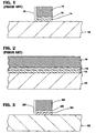
- FIG. 1 therein is shown a cross-sectional view of an exemplary conventional tungsten gate electrode stack 10 fabricated on a semiconductor substrate 12.
- the gate electrode stack 10 is commonly used as a switching device for a field effect transistor the other components of which are not shown for simplicity of illustration.
- the stack 10 consists of a gate dielectric layer 14 positioned on the substrate 12, an adhesion or glue layer 16 formed on the gate dielectric layer 14 and a tungsten gate electrode 18 formed on the adhesion layer 16.
- the substrate 12 is composed of silicon while the gate dielectric layer 14 is composed of an oxide of silicon.
- the adhesion layer 16 is composed of a titanium-based material, such as TiN.
- the gate dielectric layer 14 is initially established on the silicon substrate 12 by thermal oxidation or chemical vapor deposition. Oxide has been and continues to be a principal material of choice for gate dielectric layers in transistor fabrication due to its acceptable electrically insulating properties and relative ease of fabrication. However, the relatively poor adhesion characteristics of CVD tungsten to oxide necessitates the fabrication of the adhesion layer 16 on the gate dielectric layer 14 prior to the deposition of the tungsten layer 18. In this regard, titanium or titanium nitride is deposited on the gate dielectric layer 14 by physical vapor deposition or CVD as the case may be.
- the titanium-based adhesion layer 16 will readily adhere to the underlying oxide layer 14, and the later deposited tungsten layer 18 will readily adhere to the titanium-based adhesion layer 16.
- the adhesion layer 16 is a laminate of an underlying titanium layer and an overlying titanium nitride layer.
- the tungsten electrode layer 18 is next deposited on the adhesion layer 16 in a CVD process involving the reduction of WF 6 gas in the presence of SiH 4 and H 2 gas.
- the reducing ambient is initially primarily silane.
- the percentage of silane is reduced and the percentage of hydrogen is correspondingly increased to complete the reduction and deposition process.
- the result is the formation of a polycrystalline tungsten film 18 on the adhesion layer 16.
- the difficulty with this conventional approach for fabricating a tungsten gate electrode stack is the propensity for the adhesion layer 16 to delaminate from the underlying gate dielectric layer 14 as a result of the formation of TiF x compounds in the adhesion layer 16.
- the formation of TiF x compounds is an unwanted by product of the diffusion of fluorine atoms from the WF 6 reduction process into the adhesion layer 16.
- the diffused fluorine atoms may readily react with the highly reactive titanium, which is present in the layer 16 as elemental titanium, as titanium nitride or both.
- the tungsten film 18 is subsequently masked and anisotropically etched to yield the completed gate electrode stack 10 depicted in FIG. 1.
- the aforementioned delamination may result in unacceptably high resistivity for the gate electrode stack 10 or in catastrophic failure of the device associated with the gate electrode stack 10.
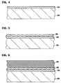
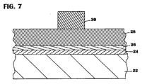
- FIG. 3 is a cross-sectional view of the gate electrode stack 20 fabricated on a semiconductor substrate 22.
- the gate electrode stack 20 consists of a gate insulating layer 24 fabricated on the semiconductor substrate 22, a tungsten silicide adhesion layer 26 positioned on the gate insulating layer 24 and a tungsten gate electrode 28 positioned on the adhesion layer 26.
- the tungsten silicide adhesion layer 26 contains a sufficient amount of unbonded silicon atoms which adhere to the underlying gate insulating layer 24, and a majority concentration of tungsten silicide to which the overlying tungsten gate electrode 28 readily adheres.
- the gate insulating layer or film 24 is fabricated on the semiconductor substrate 22.
- the substrate 22 may be composed of p-doped silicon, n-doped silicon, silicon-on-insulator or other suitable substrate materials.
- the gate insulating film 24 may be composed of oxide, silicon nitride, laminates of these or other well known gate insulating film materials and may be fabricated by oxidation, CVD or other well known techniques.
- the gate insulating layer 24 is composed of oxide with a thickness of about 10 to 200 ⁇ (1 to 20nm) and is fabricated by dry oxidation of the silicon substrate 22.
- FIGS. 5 and 6 depict two stages of a CVD reduction of WF 6 in silane.
- a mixture of WF 6 and SiH 4 is flowed over the gate insulating layer 24 for a relatively short period of time at a chamber temperature of about 300 to 400°C and pressure of about 100 to 300 mtorr (13 to 40Pa).
- the SiH 4 -to-WF 6 ratio is kept high enough to produce a deposition of a combination of amorphous silicon ( ⁇ -Si) and amorphous tungsten ( ⁇ -W).
- the purpose of the high SiH 4 -to-WF 6 ratio is to ensure that the deposition produces ⁇ -Si and ⁇ a-W along with a sufficient amount of unbonded silicon atoms. It is desirable for silicon to be present in the film 26 in non-stoichiometric quantities relative to the tungsten so that a subsequently performed anneal to convert the ⁇ -W to tungsten silicide does not consume all of the available ⁇ -Si. The unbonded silicon remaining after the anneal will enable the film 26 to readily adhere to the underlying insulating film 24.
- the flow of SiH 4 is greatly reduced while the flow of WF 6 is continued to produce the film 28 of polycrystalline tungsten as shown in FIG. 6.
- the polycrystalline structure will yield more favorable resistivity than a more amorphous grain structure.
- the film 28 will be deposited to a greater thickness than the ⁇ -Si and ⁇ -W film 26, although the thicknesses of both films 26 and 28 are largely matters of design discretion.
- the tungsten film 28 will have a thickness that is approximately twenty times the thickness of the underlying adhesion layer 26.
- the requisite flow periods for the high and low SiH 4 -to-WF 6 ratio flows will depend in large part on the particular type of tool used, the desired thicknesses for the films 26 and 28 and the desired deposition rates.
- Experiment in an Applied Materials Endura tool set to yield deposition rates of between about 10 A/s and 200 A/s (1 nm/s and 20 nm/s) has shown that an initial flow of SiH 4 and WF 6 with a SiH 4 -to-WF 6 ratio of greater that about 2:1 yields an ⁇ -Si and ⁇ -W film 26 with a sufficient amount of free silicon therein, and a subsequent flow of SiH 4 and WF 6 with a SiH 4 -to-WF 6 ratio of less than about 1:2 yields a good quality polycrystalline tungsten film 28.
- the 2:1 SiH 4 -to-WF 6 ratio flow may be carried out for about 20 seconds and the 1:2 SiH 4 -to-WF 6 ratio flow for about 400 seconds.
- a suitable lithographic mask 38 composed of well known resist or other masking materials is patterned, that is, exposed and developed to yield the desired shape of the later formed gate electrode stack 20 depicted in FIG. 3.
- the tungsten film 28, the underlying adhesion layer 26 and the gate insulating layer 24 are next anisotropically etched to yield the gate electrode stack 20 depicted in FIG. 3.
- the etch is advantageously a fluorinated plasma etch using, for example,CF 4 /O 2 with argon as a diluent gas.
- the substrate 22 is next annealed at about 500 to 1100°C.
- the anneal produces a chemical reaction between the ⁇ -Si and the ⁇ -W in the film 26 which produces tungsten silicide with the generic chemical formula W X Si Y , specific examples of which may be W 5 Si 3 and Wsi 2 .
- W X Si Y specific examples of which may be W 5 Si 3 and Wsi 2 .
- the anneal also increases the average grain size of the overlying polycrystalline tungsten electrode 28 which results in an improvement in the electrical resistivity thereof.
- the anneal may be performed for about 30 to 90 minutes in a furnace process or for about 5 to 75 seconds in a rapid thermal anneal process.
- the anneal may be performed prior to the patterning of the gate electrode stack 20.
- the anneal may be performed on the blanket films 24 ,26 and 28 depicted in FIG. 7 and the aforementioned anisotropic etch performed thereafter.
- the process of the present invention eliminates titanium as an adhesion layer material, thus eliminating the potential for delamination due to titanium-fluorine reactions.
- the process of the present invention provides for the seamless production of a tungsten gate electrode and underlying adhesion layer by merely changing the ratio of WF6 and silane flows into the CVD chamber. In this way, a separate process for establishing a titanium based adhesion layer, which ordinarily requires the use of a separate tool and workpiece movements for depositing both tungsten and titanium is eliminated.
Landscapes
- Engineering & Computer Science (AREA)
- Physics & Mathematics (AREA)
- Condensed Matter Physics & Semiconductors (AREA)
- General Physics & Mathematics (AREA)
- Manufacturing & Machinery (AREA)
- Computer Hardware Design (AREA)
- Microelectronics & Electronic Packaging (AREA)
- Power Engineering (AREA)
- Electrodes Of Semiconductors (AREA)
- Insulated Gate Type Field-Effect Transistor (AREA)
Applications Claiming Priority (3)
| Application Number | Priority Date | Filing Date | Title |
|---|---|---|---|
| US489169 | 2000-01-21 | ||
| US09/489,169 US6284636B1 (en) | 2000-01-21 | 2000-01-21 | Tungsten gate method and apparatus |
| PCT/US2000/022505 WO2001054177A1 (en) | 2000-01-21 | 2000-08-16 | Tungsten gate electrode method and device |
Publications (2)
| Publication Number | Publication Date |
|---|---|
| EP1258033A1 EP1258033A1 (en) | 2002-11-20 |
| EP1258033B1 true EP1258033B1 (en) | 2007-12-05 |
Family
ID=23942694
Family Applications (1)
| Application Number | Title | Priority Date | Filing Date |
|---|---|---|---|
| EP00955608A Expired - Lifetime EP1258033B1 (en) | 2000-01-21 | 2000-08-16 | Tungsten gate electrode method |
Country Status (6)
| Country | Link |
|---|---|
| US (1) | US6284636B1 (enExample) |
| EP (1) | EP1258033B1 (enExample) |
| JP (1) | JP2003520445A (enExample) |
| KR (1) | KR100682643B1 (enExample) |
| DE (1) | DE60037337T2 (enExample) |
| WO (1) | WO2001054177A1 (enExample) |
Families Citing this family (10)
| Publication number | Priority date | Publication date | Assignee | Title |
|---|---|---|---|---|
| US6548389B2 (en) * | 2000-04-03 | 2003-04-15 | Matsushita Electric Industrial Co., Ltd. | Semiconductor device and method for fabricating the same |
| DE10123510A1 (de) * | 2001-05-15 | 2002-11-28 | Infineon Technologies Ag | Herstellungsverfahren für ein Halbleiterbauelement |
| US6933243B2 (en) * | 2002-02-06 | 2005-08-23 | Applied Materials, Inc. | High selectivity and residue free process for metal on thin dielectric gate etch application |
| US6835659B2 (en) * | 2002-06-04 | 2004-12-28 | Micron Technology, Inc. | Electrical coupling stack and processes for making same |
| US20040061190A1 (en) | 2002-09-30 | 2004-04-01 | International Business Machines Corporation | Method and structure for tungsten gate metal surface treatment while preventing oxidation |
| KR100587686B1 (ko) * | 2004-07-15 | 2006-06-08 | 삼성전자주식회사 | 질화 티타늄막 형성방법 및 이를 이용한 커패시터 제조방법 |
| KR100939777B1 (ko) * | 2007-11-30 | 2010-01-29 | 주식회사 하이닉스반도체 | 텅스텐막 형성방법 및 이를 이용한 반도체 소자의 배선형성방법 |
| US9034716B2 (en) | 2013-01-31 | 2015-05-19 | Taiwan Semiconductor Manufacturing Company, Ltd. | Method of making a FinFET device |
| US20170309490A1 (en) * | 2014-09-24 | 2017-10-26 | Hitachi Kokusai Electric Inc. | Method of manufacturing semiconductor device |
| US10861701B2 (en) * | 2015-06-29 | 2020-12-08 | Taiwan Semiconductor Manufacturing Co., Ltd. | Semiconductor device and manufacturing method thereof |
Family Cites Families (22)
| Publication number | Priority date | Publication date | Assignee | Title |
|---|---|---|---|---|
| GB2061615A (en) | 1979-10-25 | 1981-05-13 | Gen Electric | Composite conductors for integrated circuits |
| JPS584975A (ja) | 1981-06-30 | 1983-01-12 | Fujitsu Ltd | 半導体装置の製造方法 |
| FR2578272B1 (fr) * | 1985-03-01 | 1987-05-22 | Centre Nat Rech Scient | Procede de formation sur un substrat d'une couche de siliciure de tungstene, utilisable notamment pour la realisation de couches d'interconnexion des circuits integres. |
| US5223455A (en) | 1987-07-10 | 1993-06-29 | Kabushiki Kaisha Toshiba | Method of forming refractory metal film |
| US5071788A (en) | 1988-02-18 | 1991-12-10 | International Business Machines Corporation | Method for depositing tungsten on silicon in a non-self-limiting CVD process and semiconductor device manufactured thereby |
| JP2844693B2 (ja) * | 1989-07-13 | 1999-01-06 | ソニー株式会社 | 高融点金属膜の形成方法 |
| US5158903A (en) * | 1989-11-01 | 1992-10-27 | Matsushita Electric Industrial Co., Ltd. | Method for producing a field-effect type semiconductor device |
| JPH03218637A (ja) * | 1989-11-01 | 1991-09-26 | Matsushita Electric Ind Co Ltd | 電界効果型半導体装置とその製造方法 |
| EP0498580A1 (en) | 1991-02-04 | 1992-08-12 | Canon Kabushiki Kaisha | Method for depositing a metal film containing aluminium by use of alkylaluminium halide |
| JPH04340766A (ja) * | 1991-05-17 | 1992-11-27 | Seiko Instr Inc | 半導体装置およびその製造方法 |
| JP2889430B2 (ja) * | 1992-05-14 | 1999-05-10 | シャープ株式会社 | コンタクト部形成方法 |
| JPH0637042A (ja) * | 1992-07-20 | 1994-02-10 | Hitachi Ltd | 半導体集積回路装置及びその製造方法 |
| JPH0669498A (ja) * | 1992-08-20 | 1994-03-11 | Matsushita Electron Corp | 半導体装置およびその製造方法 |
| GB9219281D0 (en) | 1992-09-11 | 1992-10-28 | Inmos Ltd | Manufacture of semiconductor devices |
| JPH06291082A (ja) * | 1993-04-06 | 1994-10-18 | Nippon Steel Corp | 半導体装置及びその製造方法 |
| JPH07263674A (ja) | 1994-03-17 | 1995-10-13 | Fujitsu Ltd | 電界効果型半導体装置とその製造方法 |
| US5472896A (en) * | 1994-11-14 | 1995-12-05 | United Microelectronics Corp. | Method for fabricating polycide gate MOSFET devices |
| JP2839076B2 (ja) | 1995-05-11 | 1998-12-16 | 日本電気株式会社 | 半導体装置およびその製造方法 |
| US5906866A (en) | 1997-02-10 | 1999-05-25 | Tokyo Electron Limited | Process for chemical vapor deposition of tungsten onto a titanium nitride substrate surface |
| US5795824A (en) | 1997-08-28 | 1998-08-18 | Novellus Systems, Inc. | Method for nucleation of CVD tungsten films |
| US6066366A (en) | 1998-07-22 | 2000-05-23 | Applied Materials, Inc. | Method for depositing uniform tungsten layers by CVD |
| US6037263A (en) | 1998-11-05 | 2000-03-14 | Vanguard International Semiconductor Corporation | Plasma enhanced CVD deposition of tungsten and tungsten compounds |
-
2000
- 2000-01-21 US US09/489,169 patent/US6284636B1/en not_active Expired - Lifetime
- 2000-08-16 EP EP00955608A patent/EP1258033B1/en not_active Expired - Lifetime
- 2000-08-16 WO PCT/US2000/022505 patent/WO2001054177A1/en not_active Ceased
- 2000-08-16 KR KR1020027009377A patent/KR100682643B1/ko not_active Expired - Fee Related
- 2000-08-16 DE DE60037337T patent/DE60037337T2/de not_active Expired - Lifetime
- 2000-08-16 JP JP2001553570A patent/JP2003520445A/ja active Pending
Non-Patent Citations (1)
| Title |
|---|
| BERNARD C.; MADAR R.; PAULEAU Y.: "CHEMICAL VAPOR DEPOSITION OF REFRACTORY METAL SILICIDES FOR VLSI METALLIZATION", SOLID STATE TECHNOLOGY, vol. 32, no. 2, 1 February 1989 (1989-02-01), TULSA, OK, US, pages 79 - 84, XP000027982 * |
Also Published As
| Publication number | Publication date |
|---|---|
| JP2003520445A (ja) | 2003-07-02 |
| KR100682643B1 (ko) | 2007-02-15 |
| DE60037337T2 (de) | 2008-11-27 |
| WO2001054177A1 (en) | 2001-07-26 |
| EP1258033A1 (en) | 2002-11-20 |
| DE60037337D1 (de) | 2008-01-17 |
| KR20020071959A (ko) | 2002-09-13 |
| US6284636B1 (en) | 2001-09-04 |
Similar Documents
| Publication | Publication Date | Title |
|---|---|---|
| US6506676B2 (en) | Method of manufacturing semiconductor devices with titanium aluminum nitride work function | |
| US7528450B2 (en) | Semiconductor device having NMOSFET and PMOSFET and manufacturing method therefor | |
| EP0908934B1 (en) | Method of manufacturing a gate electrode | |
| US20100052079A1 (en) | Semiconductor devices and fabrication process thereof | |
| US6858934B2 (en) | Semiconductor device structures including metal silicide interconnect structures that extend at least partially over transistor gate structures and methods for making the same | |
| US6100188A (en) | Stable and low resistance metal/barrier/silicon stack structure and related process for manufacturing | |
| US7638433B2 (en) | Semiconductor device and method of fabricating the same | |
| EP1258033B1 (en) | Tungsten gate electrode method | |
| JP3553725B2 (ja) | Mosトランジスタ及びその製造方法 | |
| KR100755121B1 (ko) | 전극구조체의 형성방법 및 반도체장치의 제조방법 | |
| US5958508A (en) | Process for forming a semiconductor device | |
| US6432817B1 (en) | Tungsten silicide barrier for nickel silicidation of a gate electrode | |
| US20090045469A1 (en) | Semiconductor Device and Manufacturing Method Thereof | |
| US6383880B1 (en) | NH3/N2-plasma treatment for reduced nickel silicide bridging | |
| US7880242B2 (en) | Semiconductor device and method of fabricating the same | |
| US6274472B1 (en) | Tungsten interconnect method | |
| US20090101984A1 (en) | Semiconductor device having gate electrode including metal layer and method of manufacturing the same | |
| KR100706823B1 (ko) | 티타늄나이트라이드막을 이용한 확산방지막과오믹콘택층의 동시 형성 방법 | |
| US6730587B1 (en) | Titanium barrier for nickel silicidation of a gate electrode | |
| KR100764341B1 (ko) | 반도체소자의 제조방법 | |
| KR100414229B1 (ko) | 티타늄나이트라이드막을 이용한 확산방지막과오믹콘택층의 동시 형성 방법 | |
| KR100265598B1 (ko) | 반도체소자의 게이트전극 제조방법 | |
| WO2023196505A1 (en) | Silicidation process for semiconductor devices | |
| KR100988807B1 (ko) | 저저항 폴리사이드 게이트전극 및 그 제조 방법 | |
| KR20010008583A (ko) | 반도체소자의 금속 게이트전극 형성방법 |
Legal Events
| Date | Code | Title | Description |
|---|---|---|---|
| PUAI | Public reference made under article 153(3) epc to a published international application that has entered the european phase |
Free format text: ORIGINAL CODE: 0009012 |
|
| 17P | Request for examination filed |
Effective date: 20020724 |
|
| AK | Designated contracting states |
Kind code of ref document: A1 Designated state(s): AT BE CH CY DE DK ES FI FR GB GR IE IT LI LU MC NL PT SE |
|
| RBV | Designated contracting states (corrected) |
Designated state(s): AT BE DE GB |
|
| 17Q | First examination report despatched |
Effective date: 20060406 |
|
| RTI1 | Title (correction) |
Free format text: TUNGSTEN GATE ELECTRODE METHOD |
|
| GRAP | Despatch of communication of intention to grant a patent |
Free format text: ORIGINAL CODE: EPIDOSNIGR1 |
|
| RBV | Designated contracting states (corrected) |
Designated state(s): DE GB |
|
| GRAS | Grant fee paid |
Free format text: ORIGINAL CODE: EPIDOSNIGR3 |
|
| GRAA | (expected) grant |
Free format text: ORIGINAL CODE: 0009210 |
|
| AK | Designated contracting states |
Kind code of ref document: B1 Designated state(s): DE GB |
|
| REG | Reference to a national code |
Ref country code: GB Ref legal event code: FG4D |
|
| REF | Corresponds to: |
Ref document number: 60037337 Country of ref document: DE Date of ref document: 20080117 Kind code of ref document: P |
|
| PLBE | No opposition filed within time limit |
Free format text: ORIGINAL CODE: 0009261 |
|
| STAA | Information on the status of an ep patent application or granted ep patent |
Free format text: STATUS: NO OPPOSITION FILED WITHIN TIME LIMIT |
|
| 26N | No opposition filed |
Effective date: 20080908 |
|
| REG | Reference to a national code |
Ref country code: GB Ref legal event code: 732E Free format text: REGISTERED BETWEEN 20091210 AND 20091216 |
|
| PGFP | Annual fee paid to national office [announced via postgrant information from national office to epo] |
Ref country code: GB Payment date: 20100708 Year of fee payment: 11 |
|
| PGFP | Annual fee paid to national office [announced via postgrant information from national office to epo] |
Ref country code: DE Payment date: 20110810 Year of fee payment: 12 |
|
| GBPC | Gb: european patent ceased through non-payment of renewal fee |
Effective date: 20110816 |
|
| PG25 | Lapsed in a contracting state [announced via postgrant information from national office to epo] |
Ref country code: GB Free format text: LAPSE BECAUSE OF NON-PAYMENT OF DUE FEES Effective date: 20110816 |
|
| PG25 | Lapsed in a contracting state [announced via postgrant information from national office to epo] |
Ref country code: DE Free format text: LAPSE BECAUSE OF NON-PAYMENT OF DUE FEES Effective date: 20130301 |
|
| REG | Reference to a national code |
Ref country code: DE Ref legal event code: R119 Ref document number: 60037337 Country of ref document: DE Effective date: 20130301 |