EP1250723B1 - Antenne destinee a un terminal de communication - Google Patents
Antenne destinee a un terminal de communication Download PDFInfo
- Publication number
- EP1250723B1 EP1250723B1 EP00990548A EP00990548A EP1250723B1 EP 1250723 B1 EP1250723 B1 EP 1250723B1 EP 00990548 A EP00990548 A EP 00990548A EP 00990548 A EP00990548 A EP 00990548A EP 1250723 B1 EP1250723 B1 EP 1250723B1
- Authority
- EP
- European Patent Office
- Prior art keywords
- conductor track
- track structure
- structure part
- antenna
- conductor
- Prior art date
- Legal status (The legal status is an assumption and is not a legal conclusion. Google has not performed a legal analysis and makes no representation as to the accuracy of the status listed.)
- Expired - Lifetime
Links
Images

Classifications
-
- H—ELECTRICITY
- H01—ELECTRIC ELEMENTS
- H01Q—ANTENNAS, i.e. RADIO AERIALS
- H01Q9/00—Electrically-short antennas having dimensions not more than twice the operating wavelength and consisting of conductive active radiating elements
- H01Q9/04—Resonant antennas
- H01Q9/30—Resonant antennas with feed to end of elongated active element, e.g. unipole
- H01Q9/42—Resonant antennas with feed to end of elongated active element, e.g. unipole with folded element, the folded parts being spaced apart a small fraction of the operating wavelength
-
- H—ELECTRICITY
- H01—ELECTRIC ELEMENTS
- H01Q—ANTENNAS, i.e. RADIO AERIALS
- H01Q1/00—Details of, or arrangements associated with, antennas
- H01Q1/12—Supports; Mounting means
- H01Q1/22—Supports; Mounting means by structural association with other equipment or articles
- H01Q1/24—Supports; Mounting means by structural association with other equipment or articles with receiving set
- H01Q1/241—Supports; Mounting means by structural association with other equipment or articles with receiving set used in mobile communications, e.g. GSM
- H01Q1/242—Supports; Mounting means by structural association with other equipment or articles with receiving set used in mobile communications, e.g. GSM specially adapted for hand-held use
- H01Q1/243—Supports; Mounting means by structural association with other equipment or articles with receiving set used in mobile communications, e.g. GSM specially adapted for hand-held use with built-in antennas
-
- H—ELECTRICITY
- H01—ELECTRIC ELEMENTS
- H01Q—ANTENNAS, i.e. RADIO AERIALS
- H01Q1/00—Details of, or arrangements associated with, antennas
- H01Q1/36—Structural form of radiating elements, e.g. cone, spiral, umbrella; Particular materials used therewith
-
- H—ELECTRICITY
- H01—ELECTRIC ELEMENTS
- H01Q—ANTENNAS, i.e. RADIO AERIALS
- H01Q1/00—Details of, or arrangements associated with, antennas
- H01Q1/36—Structural form of radiating elements, e.g. cone, spiral, umbrella; Particular materials used therewith
- H01Q1/38—Structural form of radiating elements, e.g. cone, spiral, umbrella; Particular materials used therewith formed by a conductive layer on an insulating support
-
- H—ELECTRICITY
- H01—ELECTRIC ELEMENTS
- H01Q—ANTENNAS, i.e. RADIO AERIALS
- H01Q5/00—Arrangements for simultaneous operation of antennas on two or more different wavebands, e.g. dual-band or multi-band arrangements
- H01Q5/30—Arrangements for providing operation on different wavebands
- H01Q5/307—Individual or coupled radiating elements, each element being fed in an unspecified way
- H01Q5/342—Individual or coupled radiating elements, each element being fed in an unspecified way for different propagation modes
- H01Q5/357—Individual or coupled radiating elements, each element being fed in an unspecified way for different propagation modes using a single feed point
- H01Q5/364—Creating multiple current paths
- H01Q5/371—Branching current paths
-
- H—ELECTRICITY
- H01—ELECTRIC ELEMENTS
- H01Q—ANTENNAS, i.e. RADIO AERIALS
- H01Q5/00—Arrangements for simultaneous operation of antennas on two or more different wavebands, e.g. dual-band or multi-band arrangements
- H01Q5/30—Arrangements for providing operation on different wavebands
- H01Q5/378—Combination of fed elements with parasitic elements
-
- H—ELECTRICITY
- H01—ELECTRIC ELEMENTS
- H01Q—ANTENNAS, i.e. RADIO AERIALS
- H01Q9/00—Electrically-short antennas having dimensions not more than twice the operating wavelength and consisting of conductive active radiating elements
- H01Q9/04—Resonant antennas
- H01Q9/30—Resonant antennas with feed to end of elongated active element, e.g. unipole
- H01Q9/40—Element having extended radiating surface
Definitions
- the invention relates to an antenna for a communication terminal with an applied on or in a carrier Conductor structure and a communication terminal with a such antenna.
- antennas are used, the only a short distance from the case protrude. These "stub antennas” have the disadvantage that they are mechanically sensitive and can break off. About that In addition, for design reasons, the antennas as possible completely optically in the miniaturized housing disappear.
- One way to fully connect antennas integrate consists of antennas of the aforementioned Type with a conductor track structure applied in or on a carrier, for example, so-called “PCB antennas” (Printed Circuit Board - Antennas).
- Such an integrated antenna must be able to cover the entire bandwidth of the respective radio channel.
- GSM 900 MHz band in the Range from 880 to 915 MHz and in the range of 925 to 960 MHz, so that the antenna covers the range of 880 must cover well up to 960 MHz.
- GSM 900 MHz band in the Range from 880 to 915 MHz and in the range of 925 to 960 MHz, so that the antenna covers the range of 880 must cover well up to 960 MHz.
- GSM 900 MHz band in the Range from 880 to 915 MHz and in the range of 925 to 960 MHz
- 880 must cover well up to 960 MHz.
- Displacement of the resonance frequency must accordingly be compensated that the antenna is still broadband than the required frequency band is, so that synonymous with a Shifting of the resonant frequency worked throughout the band can be.
- broadband antennas usually arise then, if they are geometrically big, what the Objective for a miniaturized antenna runs counter.
- an ideal antenna would have an effective antenna Length of a multiple of a quarter wavelength ( ⁇ / 4) the center frequency, in the case of the GSM 900 MHz band of 920 MHz. This length is due to the space in the housing often not available.
- the Antenna device has a first antenna part and a in the same plane above the first antenna part arranged on the second antenna part.
- a capacitive load according to the invention at the end of the first Track structure part leads to an improvement of Power distribution of the antenna.
- the capacitive load causes this is a virtual extension of the entire antenna, so that the deviation of the effective length from the ideal length can be compensated by the capacitive load.
- the "Height" of the antenna is not increased, since the Detour lines of the capacitive load predominantly across the height extend.
- the capacitive load thus has a similar effect as those from the field of "normal" radio antenna construction well-known roof capacities, which at the upper end of on Buildings, etc., erected vertical monopole rod antennas are arranged, but in addition to note here is that due to the small geometric dimensions and close to the shield cover, the board, the battery pack or other parts of the device against unavoidable capacity the mass of the device will occur and it will also cause the said upsets come through the user's hand.
- the two conductor track structure parts can in principle be relative arbitrary to the technical specifications as well as the available be adapted to the existing spatial dimensions.
- the second However, trace element part should be substantially extend transversely to the first printed conductor structure part.
- the first Conductor structure part corresponds to the rod antenna with a main extension direction, which at "normal" broadcast antenna construction the vertical direction represents; the second trace structure part corresponds to the horizontal roof capacity.
- the first Conductor structure part in this case an elongated Trace on, which ends up forming the second Ladder Structure Part forks.
- the second interconnect structure part preferably has one forming a T-bar at the end of the first trace structure part extending conductor track section.
- the second interconnect structure part in the The simplest case is the second interconnect structure part only from this one track section, so that in total the conductor track structure has a simple T-shape.
- the second interconnect structure part in order to adapt the roof capacity precisely, also meandering or meandered on certain sections be.
- the second conductor structure part symmetrical with respect to the first trace structure part or asymmetric.
- the second Track structure part performs an asymmetry in the second Track structure part to that due to the two different from the first interconnect structure part spaced reflection points at the ends of the roof capacity a superposition of two waves with slightly different Phase occurs. This leads on the one hand a reduction in the quality of the antenna, but on the other hand too a desirable increase in bandwidth.
- the conductor track structure can be designed so that the first Conductor structure part in the second conductor structure part opposite end portion of a connecting element, For example, has a contact pad, with the over a Contact spring a connection to the transmitting / receiving device the communication terminal takes place.
- This connection point corresponds to the base of a vertical antenna with Top capacity.
- the first Conductor structure part at both ends with a second Conductor structure part is loaded capacitively. In this Case, the power in the antenna in the first Conductor structure part coupled capacitively or inductively.
- the antenna as so-called “multi-band antenna” in can work in different frequency ranges
- the others Conductor structure here is capacitive or inductive with coupled to the first interconnect structure.
- it is the carrier to a board, which on one surface the first conductor track structure and on the opposite surface of a second interconnect structure having.
- the first Conductor structure part of the first interconnect structure one end the connection element, for example the contact pad, on, and the first trace structure part of the other Track structure is at both ends by a second Conductor structure part capacitively loaded.
- the Conductor structures or any other Conductor structure with respect to the main extension direction of the each first interconnect structure part parallel to each other oriented, that is, the "vertical" antenna parts lie each substantially parallel, since on this piece the Overcoupling mainly takes place.
- the main application area of the antennas 10 according to the invention is in the range of mobile phones 1 and here too especially because of the problems of covering the antenna with the hand of the user offers particularly great benefits is in the following embodiments of antennas for Mobile phones go out. It will be on it again noted that the use of such antennas of course not limited to mobile phones.
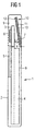
- FIG. 1 shows such a typical mobile phone 1 with a Housing 2 and an integrated antenna according to the invention 10.
- the other components of the mobile phone 1 are only partially and schematically shown.
- the mobile phone points on the one hand a motherboard 3, on the top the earpiece 6 and below the display 5 are arranged.
- Below the display 5 is the keyboard (not ) Shown.
- On the back of the motherboard 3 is under other the battery pack 4 is arranged.
- the motherboard 3 and the Battery pack 4 are usually made by a shield cover 8 shielded electrically conductive material.
- a shield cover 8 shielded electrically conductive material.
- This antenna 10 essentially consists of a carrier 11 and one on the main board 3 facing front the carrier 11 located first interconnect structure 12 and a arranged on the back second wiring structure 13th
- the antenna 10 consists essentially of a double-sided board, on which side by a conventional etching process, the conductor track structure 12, 13 generates has been.
- the wiring patterns on printed on both sides or in another suitable manner applied to a suitable carrier 11 be.
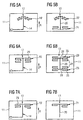
- the first wiring pattern 12 is on the Front of an antenna according to a first Embodiment shown.
- the first printed conductor structure 12 here consists of a first Track structure part 14, which in turn consists of a parallel to the longitudinal axis of the mobile phone 1, "vertical” track section 17 and at the bottom of a “horizontal” track section 18 consists.
- the first, “vertical” track section 17 has at the top End as roof capacity the second trace structure part 15th on.
- the second, “horizontal” track section 18 of the first conductor pattern part 14 serves to the lower End of the first conductor section 17 with the contact pad 19 to connect, which left in the plan view lower corner of the carrier 11 is arranged.
- This Contact pad 19 is the antenna 1 via a contact spring 7 with a corresponding lead on the motherboard 3 to a transmitting / receiving unit (not shown) connected (see Figure 1).
- the contact spring 7 bridges in present embodiment, a distance a of about 6 up to 12 mm.
- the contact pad 19 is shown in the same place. These However, position is only by the structure of the respective Mobile phones 1 conditionally.
- the contact pad can of course also at any other place, for example in the middle below or in the lower right corner of the Be arranged carrier 11.
- the entire first conductor structure part 14 forms here, starting from the extraction point to the transmitting / receiving unit, as a so-called “foot point", to the upper end, a monopole antenna, which is almost the same in broadcast antenna construction known “rod antenna” corresponds. End is this "Rod antenna” through the second printed conductor structure part 15 loaded capacitively.
- this "roofing capacity" 15 is the conductor track section 17 auf integratedd end, that is, the second Printed conductor structure part 15 has a printed conductor section 29 on, which looks like a T-bar at the end of the track section 17 of the first conductor pattern part 14 extends.
- the T-bar forming Track section 29 extend in a parallel to Main extension direction R of the first interconnect structure part 14, d. H. in the direction of the conductor track section 17, meandering further conductor track sections 24.
- These meander-shaped conductor track sections 24 consist turn from straight, perpendicular and parallel to Track section 17 oriented, individual sections. In the illustrated embodiment, they extend from the Ends of the T-bar down, d. H. in the direction of vertical trace portion 17 of the first trace structure part 14 counter to the main extension direction R. Of course, they could also be in the direction of Main extension direction R, d. H. upwards, extend. Due to the exact shape of the meander can be especially the change the spatial extent in relation to the antenna length and thereby the capacity for the screen cover 8 and to adjust other components of the mobile phone 1 accordingly, around the antenna to the desired resonant frequency adapt.
- the second printed conductor structure part 15 is mirror-symmetrical here to the first trace portion 17 of the first Track structure part 14 executed.
- This Printed circuit pattern 13 is connected to the printed conductor structure 14 the front very similar.
- the first Printed conductor structure part 20 of this second printed conductor structure 13 corresponds to the vertical conductor track section 17th of the first interconnect structure part 14 of the interconnect structure 12 on the front.
- This first trace structure part However, 20 is at both ends with another, as Capacitive load serving trace structure part 21 provided, which here exactly the second trace structure part 15 on the front corresponds.
- the antenna part is on the front, d. H. the conductor track structure 12, so executed, a resonant frequency of the antenna is in the range of 900 MHz band of the GSM system is, of course the influences by the rear structure 13 are considered.
- the rear structure 13 couples Capacitive or inductive on the front structure 12 via or vice versa.
- the rear structure 13 is designed so that a second resonance on the 1800 MHz band of the GSM system lies. That is, the overall structure is designed so that the otherwise at a 3 ⁇ 4 ⁇ corresponding frequency of approx. 2700 MHz lying next higher resonance point, which a good real part, pulled down to about 1800 MHz becomes.
- the exact tuning of the resonance takes place in essentially by the conductor track structures 12, 13 on the Front and back side.
- the widths of the tracks of the first conductor structure part and the capacitive Loads are varied.
- the track width has u. a. strong influence on the quality of the antenna and consequently on the Resonance bandwidth. This also applies to simple antennas with only one antenna part.
- FIGS. 3a and 3b show somewhat modified conductor track structures 12, 13 on the front and on the back.
- the roof capacity forming second trace structure parts 15 ', 21' is not mirror-symmetrical to the main extension direction R executed. Due to the asymmetry of two reflection points at the ends of the trace structure parts 15 ', 21' therefore creates a superposition of two waves with slightly different phase angles. Although this reduces On the one hand the quality of the antenna, but on the other hand leads to a desired increase in bandwidth.
- the symmetrical case according to Figures 2a and 2b arise at each of the two ends waves with the same phase, so that these ends act as a common point of resonance. The increase in bandwidth is especially in mobile phones important in which it is the hand of the user resonances on the antenna comes.
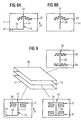
- FIGs 4a and 4b show a further embodiment an antenna 10 according to the invention.
- the first printed conductor structure parts 14, 20 respectively correspond to the Embodiments in Figures 2a to 3b. Is changed however, the shape of the second wiring pattern parts 16, 22.
- the second wiring pattern parts 16, 22 extend in each case on both sides from the end of the first printed conductor structure part 14, 20 away meandering in a substantially transverse to the first interconnect structure part 14, 20 extending Main direction. That is, the "T-bar" is here even meandering executed.
- This form of second trace structure parts 16, 22 is in both the front trace structure 12 as well as the rear Track structure 13 is carried out in this way.
- FIG. 5a shows the front side of another one Embodiment.
- the carrier 11 is cut out accordingly.
- the backside trace structure 13 is again adapted to the front trace structure 12, that is, on the upper side corresponds to the second conductor structure part 22 'of the second conductor pattern part 16' of the front Printed Circuit Structure 12.
- the Lower Second Printed Circuit Structure Part 21 is similar to the second trace structure part 21 executed according to the antenna of Figure 2b.
- FIGS. 6a and 6b An embodiment is shown in FIGS. 6a and 6b. in which the front conductor track structure 12 exactly the front Conductor 12 corresponds to the antenna of Figure 2a.
- the back conductor pattern 20 In the back conductor pattern 20, however, are the second wiring pattern parts 23 each constructed so that a meandering section 24 to the opposite end of the first conductor pattern part 20 extends and another meandering portion 25 extends outwardly. This increases the capacity additionally.
- FIGS. 7a to 8b show two different exemplary embodiments of antennas, where the rear trace structure 13 each only at one end of the first conductor track structure part 20 a second printed conductor structure part 21 ', 22 ', that is, the "vertical" part of the structure 13 is only capacitively loaded on one side.
- the fronts of the Antennas according to FIGS. 7a and 8a correspond to the antennas according to the figures 3a and 5a.
- Such one-sided capacitive Loads of the vertical element are also possible and can be useful under certain conditions. she lead, however, that the maximum current is no longer in the Center of the first conductor pattern part 20 is located.
- To one good overcoupling to the vertical conductor section 17 of the first wiring pattern part 14 of the front To obtain wiring pattern 12 is therefore the embodiment with a bilateral capacitive loading of the first Track structure part 20 on the backside trace structure 13 preferred.
- FIG. 9 shows a further multiband antenna which is suitable for three different frequency bands is provided. Accordingly The antenna is superimposed in three levels Structures 12, 13, 26.
- the first interconnect structure 12 and the second conductive pattern 13 located in the middle correspond here to the conductor track structures 12, 13 on the Front and back of the antenna according to Figures 2a and 2 B.
- the levels are arbitrarily interchangeable.
- the contact pad by the above-or underlying levels in a suitable manner to the outside be plated through.
- the Antenna according to the invention in a variety of forms executable and thus to a variety of housing and the available space adaptable.
- Prototypes by soldering or removing traces are easily changeable. Because the exact adaptation of the antenna with respect to the different resonances and the impedance of very many external, badly influenced parameters, for example, the shape of the housing, the shield cover, the depends on the motherboard components etc., the optimal structure is extremely difficult or not at all predictable. It is therefore usually in the Development of such antennas several experiments with different Prototypes required to run the device for each device find optimal antenna shape or structure, so that with The antennas according to the invention also benefits from a Reduction of development times and costs can be achieved can.
Claims (13)
- Antenne multibande (10) destinée à un terminal de communication (1), comprenant une structure à circuit conducteur (12) appliquée sur et/ou dans un porteur (11), la structure à circuit conducteur (12) présentant une première partie de structure à circuit conducteur (14), laquelle, du côté terminal, est chargée de manière capacitive au moyen d'une deuxième partie de structure à circuit conducteur (16, 16') pour la syntonisation de l'antenne (10) sur un canal radio souhaité, caractérisée en ce que l'antenne présente, pour la syntonisation sur un autre canal radio souhaité, une première partie d'antenne ayant une première structure à circuit conducteur (12) et, dans un plan situé essentiellement en parallèle à l'opposé de la première structure à circuit conducteur (12), une autre partie d'antenne munie d'une autre structure à circuit conducteur (13) appliquée sur et/ou dans le porteur (11) ou sur et/ou dans un autre porteur, cette structure à circuit conducteur étant couplée à la première structure à circuit conducteur (12) de manière capacitive et/ou inductive, l'autre structure à circuit conducteur (13) présentant une première partie de structure à circuit conducteur (20), laquelle est chargée de manière capacitive, du côté terminal, pour la syntonisation de l'antenne (10) sur un canal radio souhaité au moyen d'une autre deuxième partie de structure à circuit conducteur (22, 22'),
la deuxième partie de structure à circuit conducteur et l'autre deuxième partie de structure à circuit conducteur (16, 16', 22, 22') s'étendant essentiellement transversalement par rapport à la première partie respective de structure à circuit conducteur (14, 20), et
la deuxième partie de structure à circuit conducteur et l'autre deuxième partie de structure à circuit conducteur (16, 16', 22, 22') s'étendant respectivement des deux côtés en s'éloignant de l'extrémité de la première partie respective de structure à circuit conducteur (14, 20), en forme de méandres, dans un sens d'entendue principale passant essentiellement transversalement par rapport à la première partie de structure à circuit conducteur (14, 20) ou en forme d'arc à l'extrémité de la première partie respective de structure à circuit conducteur (14, 20). - Antenne selon la revendication 1, caractérisée en ce que la première partie de structure à circuit conducteur (14, 20, 27) présente un circuit conducteur allongé qui se divise, du côté terminal, pour former la deuxième partie de structure à circuit conducteur (15, 15', 16, 16', 21, 21', 22, 22', 23, 28).
- Antenne selon la revendication 1 ou 2, caractérisée en ce que la deuxième partie de structure à circuit conducteur (15, 15', 21, 21', 23) présente une section de circuit conducteur (29) s'étendant en formant une barre en T à l'extrémité de la première partie de structure à circuit conducteur (14, 20).
- Antenne selon la revendication 3, caractérisée en ce que la deuxième partie de structure à circuit conducteur (15, 15', 21, 21', 23) présente, respectivement sur les deux extrémités de la section de circuit conducteur (29) formant la barre en T, d'autres sections de circuit conducteur (24, 25) s'étendant en forme de méandres dans un sens d'étendue principale orienté en parallèle à la première partie de structure à circuit conducteur (14, 20).
- Antenne selon l'une quelconque des revendications précédentes, caractérisée en ce que la deuxième partie de structure à circuit conducteur (15, 21, 28) est exécutée de manière symétrique par rapport à la première partie de structure à circuit conducteur (14, 20, 27).
- Antenne selon l'une quelconque des revendications 1 à 4, caractérisée en ce que la deuxième partie de structure à circuit conducteur (15', 21') est exécutée de manière asymétrique par rapport à la première partie de structure à circuit conducteur (14, 20).
- Antenne selon l'une quelconque des revendications précédentes, caractérisée en ce que la première partie de structure à circuit conducteur (14) présente un élément de raccordement (19) dans la partie terminale opposée à la deuxième partie de structure à circuit conducteur (15, 15', 16, 16').
- Antenne selon la revendication 7, caractérisée en ce que la première partie de structure à circuit conducteur (14) présente deux sections de circuit conducteur (17, 18), la première section de circuit conducteur (17) étant chargée de manière capacitive sur une extrémité au moyen de la deuxième partie de structure à circuit conducteur (15, 15', 16, 16') et la deuxième section de circuit conducteur (18) raccordant l'autre extrémité de la première section de circuit conducteur (17) à l'élément de raccordement (19).
- Antenne selon l'une quelconque des revendications 1 à 7, caractérisée en ce que la première partie de structure à circuit conducteur (20, 27) est chargée de manière capacitive sur les deux extrémités au moyen d'une deuxième partie de structure à circuit conducteur (21, 21', 22, 22', 23, 28).
- Antenne selon l'une quelconque des revendications précédentes, caractérisée en ce que la première partie de structure à circuit conducteur (14) de la première structure à circuit conducteur (12) présente, sur une extrémité, un élément de raccordement (19) et en ce que la première partie de structure à circuit conducteur (20, 27) de l'autre structure à circuit conducteur (13, 26) présente, sur les deux extrémités, une deuxième partie de structure à circuit conducteur (21, 21', 22, 22', 23, 28) comme charge capacitive.
- Antenne selon l'une quelconque des revendications précédentes, caractérisée en ce que la première structure à circuit conducteur (12) et l'autre structure à circuit conducteur (13, 26) sont orientées essentiellement en étant parallèles l'une à l'autre, par rapport à leur première partie respective de structure à circuit conducteur (14, 20, 27).
- Terminal de communication (1) comprenant une antenne selon l'une quelconque des revendications 1 à 11.
- Terminal de communication selon la revendication 12, caractérisé en ce que le terminal est un téléphone mobile (1).
Applications Claiming Priority (3)
| Application Number | Priority Date | Filing Date | Title |
|---|---|---|---|
| DE19961488A DE19961488A1 (de) | 1999-12-20 | 1999-12-20 | Antenne für ein Kommunikationsendgerät |
| DE19961488 | 1999-12-20 | ||
| PCT/DE2000/004531 WO2001047056A2 (fr) | 1999-12-20 | 2000-12-19 | Antenne destinee a un terminal de communication |
Publications (2)
| Publication Number | Publication Date |
|---|---|
| EP1250723A2 EP1250723A2 (fr) | 2002-10-23 |
| EP1250723B1 true EP1250723B1 (fr) | 2005-03-30 |
Family
ID=7933439
Family Applications (1)
| Application Number | Title | Priority Date | Filing Date |
|---|---|---|---|
| EP00990548A Expired - Lifetime EP1250723B1 (fr) | 1999-12-20 | 2000-12-19 | Antenne destinee a un terminal de communication |
Country Status (5)
| Country | Link |
|---|---|
| US (1) | US6839040B2 (fr) |
| EP (1) | EP1250723B1 (fr) |
| CN (1) | CN1185762C (fr) |
| DE (2) | DE19961488A1 (fr) |
| WO (1) | WO2001047056A2 (fr) |
Families Citing this family (25)
| Publication number | Priority date | Publication date | Assignee | Title |
|---|---|---|---|---|
| ATE302473T1 (de) | 2000-01-19 | 2005-09-15 | Fractus Sa | Raumfüllende miniaturantenne |
| EP1298807A1 (fr) * | 2001-09-28 | 2003-04-02 | Siemens Aktiengesellschaft | Module pour transmission et/ou réception de données par radio |
| US9755314B2 (en) | 2001-10-16 | 2017-09-05 | Fractus S.A. | Loaded antenna |
| JP2003198410A (ja) * | 2001-12-27 | 2003-07-11 | Matsushita Electric Ind Co Ltd | 通信端末装置用アンテナ |
| TW557604B (en) * | 2002-05-23 | 2003-10-11 | Realtek Semiconductor Corp | Printed antenna structure |
| EP1372213A1 (fr) * | 2002-06-11 | 2003-12-17 | Industrial Technology Research Institute | Antenne multibande |
| BR0215790A (pt) | 2002-06-25 | 2005-03-01 | Fractus Sa | Antena para múltiplas faixas de sintonia |
| ATE545173T1 (de) * | 2002-12-22 | 2012-02-15 | Fractus Sa | Mehrband-monopolantenne für ein mobilfunkgerät |
| WO2004070871A1 (fr) * | 2003-02-10 | 2004-08-19 | Sony Ericsson Mobile Communications Ab | Systeme combine de haut-parleur et d'antenne |
| JP4010283B2 (ja) * | 2003-06-17 | 2007-11-21 | ミツミ電機株式会社 | アンテナ装置 |
| US6876332B1 (en) * | 2003-11-11 | 2005-04-05 | Realtek Semiconductor Corp. | Multiple-frequency antenna structure |
| DE10361634A1 (de) * | 2003-12-30 | 2005-08-04 | Advanced Micro Devices, Inc., Sunnyvale | Leistungsfähige kostengünstige Monopolantenne für Funkanwendungen |
| EP1709704A2 (fr) * | 2004-01-30 | 2006-10-11 | Fractus, S.A. | Antennes unipolaires multibandes pour dispositifs de communications mobiles |
| JP2006340367A (ja) * | 2005-06-02 | 2006-12-14 | Behavior Tech Computer Corp | 内蔵式アンテナ及びコネクタを備える無線送信装置 |
| KR100731600B1 (ko) | 2005-12-26 | 2007-06-22 | (주)에이스안테나 | 상호 보완적인 방사체 구조의 내장형 칩안테나 |
| JP3883565B1 (ja) * | 2006-02-28 | 2007-02-21 | Tdk株式会社 | チップアンテナ |
| US8738103B2 (en) | 2006-07-18 | 2014-05-27 | Fractus, S.A. | Multiple-body-configuration multimedia and smartphone multifunction wireless devices |
| EP1983467B1 (fr) * | 2007-04-19 | 2013-03-13 | BALLUFF GmbH | Dispositif de support de données/émission et procédé destiné à sa fabrication |
| FR2928037B1 (fr) * | 2008-02-21 | 2010-03-26 | Composants Electr Soc D | Antenne pour vehicule automobile, en particulier pour la reception de signaux radio terrestre et/ou satellites. |
| KR101044994B1 (ko) * | 2008-06-20 | 2011-06-29 | 삼성전자주식회사 | 휴대 단말기의 안테나 장치 |
| KR101133343B1 (ko) * | 2011-01-04 | 2012-04-06 | 인천대학교 산학협력단 | 위상 변화가 없는 mimo 안테나 |
| GB2493373A (en) * | 2011-08-03 | 2013-02-06 | Harada Ind Co Ltd | Antenna with a bent conductor for multiple frequency operation |
| US9786987B2 (en) * | 2012-09-14 | 2017-10-10 | Panasonic Intellectual Property Management Co., Ltd. | Small antenna apparatus operable in multiple frequency bands |
| US9711863B2 (en) | 2013-03-13 | 2017-07-18 | Microsoft Technology Licensing, Llc | Dual band WLAN coupled radiator antenna |
| CN112886232B (zh) * | 2019-11-30 | 2022-10-11 | 华为技术有限公司 | 电子设备 |
Citations (3)
| Publication number | Priority date | Publication date | Assignee | Title |
|---|---|---|---|---|
| WO1998038694A1 (fr) * | 1997-02-25 | 1998-09-03 | Pates Technology Patentverwertungsgesellschaft Für Satelliten- Und Moderne Informationstechnologien Mbh | Antenne accordee |
| US5809433A (en) * | 1994-09-15 | 1998-09-15 | Motorola, Inc. | Multi-component antenna and method therefor |
| EP0986130A2 (fr) * | 1998-09-08 | 2000-03-15 | Siemens Aktiengesellschaft | Antenne pour terminaux de radiocommunication sans fil |
Family Cites Families (3)
| Publication number | Priority date | Publication date | Assignee | Title |
|---|---|---|---|---|
| EP0814536A3 (fr) * | 1996-06-20 | 1999-10-13 | Kabushiki Kaisha Yokowo | Antenne et appareil de radio utilisant une telle antenne |
| EP0954054A1 (fr) * | 1998-04-30 | 1999-11-03 | Kabushiki Kaisha Yokowo | Antenne pliable |
| SE512524C2 (sv) * | 1998-06-24 | 2000-03-27 | Allgon Ab | En antennanordning, en metod för framställning av en antennenordning och en radiokommunikationsanordning inkluderande en antennanordning |
-
1999
- 1999-12-20 DE DE19961488A patent/DE19961488A1/de not_active Withdrawn
-
2000
- 2000-12-19 CN CNB008172447A patent/CN1185762C/zh not_active Expired - Fee Related
- 2000-12-19 EP EP00990548A patent/EP1250723B1/fr not_active Expired - Lifetime
- 2000-12-19 DE DE50009947T patent/DE50009947D1/de not_active Expired - Lifetime
- 2000-12-19 US US10/168,252 patent/US6839040B2/en not_active Expired - Fee Related
- 2000-12-19 WO PCT/DE2000/004531 patent/WO2001047056A2/fr active IP Right Grant
Patent Citations (3)
| Publication number | Priority date | Publication date | Assignee | Title |
|---|---|---|---|---|
| US5809433A (en) * | 1994-09-15 | 1998-09-15 | Motorola, Inc. | Multi-component antenna and method therefor |
| WO1998038694A1 (fr) * | 1997-02-25 | 1998-09-03 | Pates Technology Patentverwertungsgesellschaft Für Satelliten- Und Moderne Informationstechnologien Mbh | Antenne accordee |
| EP0986130A2 (fr) * | 1998-09-08 | 2000-03-15 | Siemens Aktiengesellschaft | Antenne pour terminaux de radiocommunication sans fil |
Also Published As
| Publication number | Publication date |
|---|---|
| WO2001047056A2 (fr) | 2001-06-28 |
| CN1411621A (zh) | 2003-04-16 |
| CN1185762C (zh) | 2005-01-19 |
| DE19961488A1 (de) | 2001-06-21 |
| DE50009947D1 (de) | 2005-05-04 |
| EP1250723A2 (fr) | 2002-10-23 |
| US6839040B2 (en) | 2005-01-04 |
| WO2001047056A3 (fr) | 2001-12-27 |
| US20040027295A1 (en) | 2004-02-12 |
Similar Documents
| Publication | Publication Date | Title |
|---|---|---|
| EP1250723B1 (fr) | Antenne destinee a un terminal de communication | |
| DE60033275T2 (de) | Oberflächenmontierbare antenne und kommunikationsgerät mit einer derartigen antenne | |
| DE60302955T2 (de) | Abstimmbare Mehrband-Planarantenne | |
| EP1195845B1 (fr) | Antenne radioélectrique miniaturisée | |
| DE60023062T2 (de) | Antennenkonstruktion | |
| DE10319093B3 (de) | Antennenvorrichtung | |
| DE60217224T2 (de) | Invertierte F-Antenne und tragbares Kommunikationsgerät mit einer solchen Antenne | |
| EP1829158B1 (fr) | Structure d'antenne disque unipolaire | |
| DE60104756T2 (de) | Oberflächenmontierte Antenne, Verfahren zur Justierung und Einstellung der Zweifrequenzresonanz der Antenne und Kommunikationsgerät mit einer derartigen Antenne | |
| DE602005002567T2 (de) | Breitbandige abstimmbare Antenne | |
| DE10143168A1 (de) | Schaltungsplatine und SMD-Antenne hierfür | |
| DE10029733A1 (de) | Antennenanordnung für Mobilfunktelefone | |
| EP1154518B1 (fr) | Antenne intégrée pour téléphones portables | |
| DE69735983T2 (de) | Antennenvorrichtung | |
| DE102007055327B4 (de) | Externes mehrbandiges Funkantennenmodul | |
| DE3339278C2 (fr) | ||
| WO2004027929A1 (fr) | Ensemble antenne pourvu d'un dipole panneau | |
| DE10209961A1 (de) | Mikrowellenantenne | |
| DE102004045006B4 (de) | Hochfrequenzfilter | |
| DE10210341A1 (de) | Mehrband-Mikrowellenantenne | |
| DE602004012377T2 (de) | Endgerät für eine mobile Kommunikation | |
| EP1198026A2 (fr) | Arrangement d'antenne pour téléphones mobiles | |
| DE10204079A1 (de) | Mehrbandantenne mit parasitären Strahlern | |
| DE19843929A1 (de) | Flachantenne | |
| DE10303540B4 (de) | Antennenanordnung |
Legal Events
| Date | Code | Title | Description |
|---|---|---|---|
| PUAI | Public reference made under article 153(3) epc to a published international application that has entered the european phase |
Free format text: ORIGINAL CODE: 0009012 |
|
| 17P | Request for examination filed |
Effective date: 20020522 |
|
| AK | Designated contracting states |
Kind code of ref document: A2 Designated state(s): AT BE CH CY DE DK ES FI FR GB GR IE IT LI LU MC NL PT SE TR |
|
| AX | Request for extension of the european patent |
Free format text: AL;LT;LV;MK;RO;SI |
|
| 17Q | First examination report despatched |
Effective date: 20030623 |
|
| RBV | Designated contracting states (corrected) |
Designated state(s): DE FR GB |
|
| GRAP | Despatch of communication of intention to grant a patent |
Free format text: ORIGINAL CODE: EPIDOSNIGR1 |
|
| RIC1 | Information provided on ipc code assigned before grant |
Ipc: 7H 01Q 1/38 B Ipc: 7H 01Q 1/00 A |
|
| RIC1 | Information provided on ipc code assigned before grant |
Ipc: 7H 01Q 1/38 A |
|
| GRAS | Grant fee paid |
Free format text: ORIGINAL CODE: EPIDOSNIGR3 |
|
| GRAA | (expected) grant |
Free format text: ORIGINAL CODE: 0009210 |
|
| RIN1 | Information on inventor provided before grant (corrected) |
Inventor name: OELSCHLAEGER, MARTIN Inventor name: SCHREIBER, MICHAEL Inventor name: HUBER, STEFAN |
|
| AK | Designated contracting states |
Kind code of ref document: B1 Designated state(s): DE FR GB |
|
| REG | Reference to a national code |
Ref country code: GB Ref legal event code: FG4D Free format text: NOT ENGLISH |
|
| REF | Corresponds to: |
Ref document number: 50009947 Country of ref document: DE Date of ref document: 20050504 Kind code of ref document: P |
|
| REG | Reference to a national code |
Ref country code: IE Ref legal event code: FG4D Free format text: LANGUAGE OF EP DOCUMENT: GERMAN |
|
| GBT | Gb: translation of ep patent filed (gb section 77(6)(a)/1977) |
Effective date: 20050425 |
|
| PLBE | No opposition filed within time limit |
Free format text: ORIGINAL CODE: 0009261 |
|
| STAA | Information on the status of an ep patent application or granted ep patent |
Free format text: STATUS: NO OPPOSITION FILED WITHIN TIME LIMIT |
|
| ET | Fr: translation filed | ||
| 26N | No opposition filed |
Effective date: 20060102 |
|
| REG | Reference to a national code |
Ref country code: GB Ref legal event code: 732E |
|
| PGFP | Annual fee paid to national office [announced via postgrant information from national office to epo] |
Ref country code: FR Payment date: 20061222 Year of fee payment: 7 |
|
| REG | Reference to a national code |
Ref country code: FR Ref legal event code: TP |
|
| REG | Reference to a national code |
Ref country code: GB Ref legal event code: 732E |
|
| REG | Reference to a national code |
Ref country code: FR Ref legal event code: ST Effective date: 20081020 |
|
| PG25 | Lapsed in a contracting state [announced via postgrant information from national office to epo] |
Ref country code: FR Free format text: LAPSE BECAUSE OF NON-PAYMENT OF DUE FEES Effective date: 20071231 |
|
| REG | Reference to a national code |
Ref country code: GB Ref legal event code: 732E Free format text: REGISTERED BETWEEN 20110407 AND 20110413 |
|
| REG | Reference to a national code |
Ref country code: DE Ref legal event code: R081 Ref document number: 50009947 Country of ref document: DE Owner name: QUALCOMM INCORPORATED, US Free format text: FORMER OWNER: PALM, INC. (N.D.GES. D. STAATES DELAWARE), SUNNYVALE, US Effective date: 20110406 Ref country code: DE Ref legal event code: R081 Ref document number: 50009947 Country of ref document: DE Owner name: QUALCOMM INCORPORATED, SAN DIEGO, US Free format text: FORMER OWNER: PALM, INC. (N.D.GES. D. STAATES DELAWARE), SUNNYVALE, CALIF., US Effective date: 20110406 |
|
| REG | Reference to a national code |
Ref country code: DE Ref legal event code: R082 Ref document number: 50009947 Country of ref document: DE Representative=s name: SAMSON & PARTNER, PATENTANWAELTE, DE |
|
| REG | Reference to a national code |
Ref country code: DE Ref legal event code: R082 Ref document number: 50009947 Country of ref document: DE Representative=s name: MAUCHER JENKINS, DE Effective date: 20140307 Ref country code: DE Ref legal event code: R081 Ref document number: 50009947 Country of ref document: DE Owner name: QUALCOMM INCORPORATED, US Free format text: FORMER OWNER: HEWLETT-PACKARD DEVELOPMENT CO., L.P., HOUSTON, US Effective date: 20140307 Ref country code: DE Ref legal event code: R082 Ref document number: 50009947 Country of ref document: DE Representative=s name: SAMSON & PARTNER, PATENTANWAELTE, DE Effective date: 20140307 Ref country code: DE Ref legal event code: R081 Ref document number: 50009947 Country of ref document: DE Owner name: QUALCOMM INCORPORATED, SAN DIEGO, US Free format text: FORMER OWNER: HEWLETT-PACKARD DEVELOPMENT COMPANY, L.P., HOUSTON, TEX., US Effective date: 20140307 Ref country code: DE Ref legal event code: R082 Ref document number: 50009947 Country of ref document: DE Representative=s name: SAMSON & PARTNER PATENTANWAELTE MBB, DE Effective date: 20140307 |
|
| REG | Reference to a national code |
Ref country code: GB Ref legal event code: 732E Free format text: REGISTERED BETWEEN 20140508 AND 20140514 |
|
| REG | Reference to a national code |
Ref country code: DE Ref legal event code: R082 Ref document number: 50009947 Country of ref document: DE Representative=s name: MAUCHER JENKINS, DE Ref country code: DE Ref legal event code: R082 Ref document number: 50009947 Country of ref document: DE Representative=s name: MAUCHER JENKINS PATENTANWAELTE & RECHTSANWAELT, DE |
|
| PGFP | Annual fee paid to national office [announced via postgrant information from national office to epo] |
Ref country code: DE Payment date: 20181114 Year of fee payment: 19 |
|
| PGFP | Annual fee paid to national office [announced via postgrant information from national office to epo] |
Ref country code: GB Payment date: 20181129 Year of fee payment: 19 |
|
| REG | Reference to a national code |
Ref country code: DE Ref legal event code: R119 Ref document number: 50009947 Country of ref document: DE |
|
| GBPC | Gb: european patent ceased through non-payment of renewal fee |
Effective date: 20191219 |
|
| PG25 | Lapsed in a contracting state [announced via postgrant information from national office to epo] |
Ref country code: GB Free format text: LAPSE BECAUSE OF NON-PAYMENT OF DUE FEES Effective date: 20191219 Ref country code: DE Free format text: LAPSE BECAUSE OF NON-PAYMENT OF DUE FEES Effective date: 20200701 |