EP1250723B1 - Antenna for a communications terminal - Google Patents
Antenna for a communications terminal Download PDFInfo
- Publication number
- EP1250723B1 EP1250723B1 EP00990548A EP00990548A EP1250723B1 EP 1250723 B1 EP1250723 B1 EP 1250723B1 EP 00990548 A EP00990548 A EP 00990548A EP 00990548 A EP00990548 A EP 00990548A EP 1250723 B1 EP1250723 B1 EP 1250723B1
- Authority
- EP
- European Patent Office
- Prior art keywords
- conductor track
- track structure
- structure part
- antenna
- conductor
- Prior art date
- Legal status (The legal status is an assumption and is not a legal conclusion. Google has not performed a legal analysis and makes no representation as to the accuracy of the status listed.)
- Expired - Lifetime
Links
Images

Classifications
-
- H—ELECTRICITY
- H01—ELECTRIC ELEMENTS
- H01Q—ANTENNAS, i.e. RADIO AERIALS
- H01Q9/00—Electrically-short antennas having dimensions not more than twice the operating wavelength and consisting of conductive active radiating elements
- H01Q9/04—Resonant antennas
- H01Q9/30—Resonant antennas with feed to end of elongated active element, e.g. unipole
- H01Q9/42—Resonant antennas with feed to end of elongated active element, e.g. unipole with folded element, the folded parts being spaced apart a small fraction of the operating wavelength
-
- H—ELECTRICITY
- H01—ELECTRIC ELEMENTS
- H01Q—ANTENNAS, i.e. RADIO AERIALS
- H01Q1/00—Details of, or arrangements associated with, antennas
- H01Q1/12—Supports; Mounting means
- H01Q1/22—Supports; Mounting means by structural association with other equipment or articles
- H01Q1/24—Supports; Mounting means by structural association with other equipment or articles with receiving set
- H01Q1/241—Supports; Mounting means by structural association with other equipment or articles with receiving set used in mobile communications, e.g. GSM
- H01Q1/242—Supports; Mounting means by structural association with other equipment or articles with receiving set used in mobile communications, e.g. GSM specially adapted for hand-held use
- H01Q1/243—Supports; Mounting means by structural association with other equipment or articles with receiving set used in mobile communications, e.g. GSM specially adapted for hand-held use with built-in antennas
-
- H—ELECTRICITY
- H01—ELECTRIC ELEMENTS
- H01Q—ANTENNAS, i.e. RADIO AERIALS
- H01Q1/00—Details of, or arrangements associated with, antennas
- H01Q1/36—Structural form of radiating elements, e.g. cone, spiral, umbrella; Particular materials used therewith
-
- H—ELECTRICITY
- H01—ELECTRIC ELEMENTS
- H01Q—ANTENNAS, i.e. RADIO AERIALS
- H01Q1/00—Details of, or arrangements associated with, antennas
- H01Q1/36—Structural form of radiating elements, e.g. cone, spiral, umbrella; Particular materials used therewith
- H01Q1/38—Structural form of radiating elements, e.g. cone, spiral, umbrella; Particular materials used therewith formed by a conductive layer on an insulating support
-
- H—ELECTRICITY
- H01—ELECTRIC ELEMENTS
- H01Q—ANTENNAS, i.e. RADIO AERIALS
- H01Q5/00—Arrangements for simultaneous operation of antennas on two or more different wavebands, e.g. dual-band or multi-band arrangements
- H01Q5/30—Arrangements for providing operation on different wavebands
- H01Q5/307—Individual or coupled radiating elements, each element being fed in an unspecified way
- H01Q5/342—Individual or coupled radiating elements, each element being fed in an unspecified way for different propagation modes
- H01Q5/357—Individual or coupled radiating elements, each element being fed in an unspecified way for different propagation modes using a single feed point
- H01Q5/364—Creating multiple current paths
- H01Q5/371—Branching current paths
-
- H—ELECTRICITY
- H01—ELECTRIC ELEMENTS
- H01Q—ANTENNAS, i.e. RADIO AERIALS
- H01Q5/00—Arrangements for simultaneous operation of antennas on two or more different wavebands, e.g. dual-band or multi-band arrangements
- H01Q5/30—Arrangements for providing operation on different wavebands
- H01Q5/378—Combination of fed elements with parasitic elements
-
- H—ELECTRICITY
- H01—ELECTRIC ELEMENTS
- H01Q—ANTENNAS, i.e. RADIO AERIALS
- H01Q9/00—Electrically-short antennas having dimensions not more than twice the operating wavelength and consisting of conductive active radiating elements
- H01Q9/04—Resonant antennas
- H01Q9/30—Resonant antennas with feed to end of elongated active element, e.g. unipole
- H01Q9/40—Element having extended radiating surface
Definitions
- the invention relates to an antenna for a communication terminal with an applied on or in a carrier Conductor structure and a communication terminal with a such antenna.
- antennas are used, the only a short distance from the case protrude. These "stub antennas” have the disadvantage that they are mechanically sensitive and can break off. About that In addition, for design reasons, the antennas as possible completely optically in the miniaturized housing disappear.
- One way to fully connect antennas integrate consists of antennas of the aforementioned Type with a conductor track structure applied in or on a carrier, for example, so-called “PCB antennas” (Printed Circuit Board - Antennas).
- Such an integrated antenna must be able to cover the entire bandwidth of the respective radio channel.
- GSM 900 MHz band in the Range from 880 to 915 MHz and in the range of 925 to 960 MHz, so that the antenna covers the range of 880 must cover well up to 960 MHz.
- GSM 900 MHz band in the Range from 880 to 915 MHz and in the range of 925 to 960 MHz, so that the antenna covers the range of 880 must cover well up to 960 MHz.
- GSM 900 MHz band in the Range from 880 to 915 MHz and in the range of 925 to 960 MHz
- 880 must cover well up to 960 MHz.
- Displacement of the resonance frequency must accordingly be compensated that the antenna is still broadband than the required frequency band is, so that synonymous with a Shifting of the resonant frequency worked throughout the band can be.
- broadband antennas usually arise then, if they are geometrically big, what the Objective for a miniaturized antenna runs counter.
- an ideal antenna would have an effective antenna Length of a multiple of a quarter wavelength ( ⁇ / 4) the center frequency, in the case of the GSM 900 MHz band of 920 MHz. This length is due to the space in the housing often not available.
- the Antenna device has a first antenna part and a in the same plane above the first antenna part arranged on the second antenna part.
- a capacitive load according to the invention at the end of the first Track structure part leads to an improvement of Power distribution of the antenna.
- the capacitive load causes this is a virtual extension of the entire antenna, so that the deviation of the effective length from the ideal length can be compensated by the capacitive load.
- the "Height" of the antenna is not increased, since the Detour lines of the capacitive load predominantly across the height extend.
- the capacitive load thus has a similar effect as those from the field of "normal" radio antenna construction well-known roof capacities, which at the upper end of on Buildings, etc., erected vertical monopole rod antennas are arranged, but in addition to note here is that due to the small geometric dimensions and close to the shield cover, the board, the battery pack or other parts of the device against unavoidable capacity the mass of the device will occur and it will also cause the said upsets come through the user's hand.
- the two conductor track structure parts can in principle be relative arbitrary to the technical specifications as well as the available be adapted to the existing spatial dimensions.
- the second However, trace element part should be substantially extend transversely to the first printed conductor structure part.
- the first Conductor structure part corresponds to the rod antenna with a main extension direction, which at "normal" broadcast antenna construction the vertical direction represents; the second trace structure part corresponds to the horizontal roof capacity.
- the first Conductor structure part in this case an elongated Trace on, which ends up forming the second Ladder Structure Part forks.
- the second interconnect structure part preferably has one forming a T-bar at the end of the first trace structure part extending conductor track section.
- the second interconnect structure part in the The simplest case is the second interconnect structure part only from this one track section, so that in total the conductor track structure has a simple T-shape.
- the second interconnect structure part in order to adapt the roof capacity precisely, also meandering or meandered on certain sections be.
- the second conductor structure part symmetrical with respect to the first trace structure part or asymmetric.
- the second Track structure part performs an asymmetry in the second Track structure part to that due to the two different from the first interconnect structure part spaced reflection points at the ends of the roof capacity a superposition of two waves with slightly different Phase occurs. This leads on the one hand a reduction in the quality of the antenna, but on the other hand too a desirable increase in bandwidth.
- the conductor track structure can be designed so that the first Conductor structure part in the second conductor structure part opposite end portion of a connecting element, For example, has a contact pad, with the over a Contact spring a connection to the transmitting / receiving device the communication terminal takes place.
- This connection point corresponds to the base of a vertical antenna with Top capacity.
- the first Conductor structure part at both ends with a second Conductor structure part is loaded capacitively. In this Case, the power in the antenna in the first Conductor structure part coupled capacitively or inductively.
- the antenna as so-called “multi-band antenna” in can work in different frequency ranges
- the others Conductor structure here is capacitive or inductive with coupled to the first interconnect structure.
- it is the carrier to a board, which on one surface the first conductor track structure and on the opposite surface of a second interconnect structure having.
- the first Conductor structure part of the first interconnect structure one end the connection element, for example the contact pad, on, and the first trace structure part of the other Track structure is at both ends by a second Conductor structure part capacitively loaded.
- the Conductor structures or any other Conductor structure with respect to the main extension direction of the each first interconnect structure part parallel to each other oriented, that is, the "vertical" antenna parts lie each substantially parallel, since on this piece the Overcoupling mainly takes place.
- the main application area of the antennas 10 according to the invention is in the range of mobile phones 1 and here too especially because of the problems of covering the antenna with the hand of the user offers particularly great benefits is in the following embodiments of antennas for Mobile phones go out. It will be on it again noted that the use of such antennas of course not limited to mobile phones.
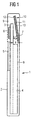
- FIG. 1 shows such a typical mobile phone 1 with a Housing 2 and an integrated antenna according to the invention 10.
- the other components of the mobile phone 1 are only partially and schematically shown.
- the mobile phone points on the one hand a motherboard 3, on the top the earpiece 6 and below the display 5 are arranged.
- Below the display 5 is the keyboard (not ) Shown.
- On the back of the motherboard 3 is under other the battery pack 4 is arranged.
- the motherboard 3 and the Battery pack 4 are usually made by a shield cover 8 shielded electrically conductive material.
- a shield cover 8 shielded electrically conductive material.
- This antenna 10 essentially consists of a carrier 11 and one on the main board 3 facing front the carrier 11 located first interconnect structure 12 and a arranged on the back second wiring structure 13th
- the antenna 10 consists essentially of a double-sided board, on which side by a conventional etching process, the conductor track structure 12, 13 generates has been.
- the wiring patterns on printed on both sides or in another suitable manner applied to a suitable carrier 11 be.
- the first wiring pattern 12 is on the Front of an antenna according to a first Embodiment shown.
- the first printed conductor structure 12 here consists of a first Track structure part 14, which in turn consists of a parallel to the longitudinal axis of the mobile phone 1, "vertical” track section 17 and at the bottom of a “horizontal” track section 18 consists.
- the first, “vertical” track section 17 has at the top End as roof capacity the second trace structure part 15th on.
- the second, “horizontal” track section 18 of the first conductor pattern part 14 serves to the lower End of the first conductor section 17 with the contact pad 19 to connect, which left in the plan view lower corner of the carrier 11 is arranged.
- This Contact pad 19 is the antenna 1 via a contact spring 7 with a corresponding lead on the motherboard 3 to a transmitting / receiving unit (not shown) connected (see Figure 1).
- the contact spring 7 bridges in present embodiment, a distance a of about 6 up to 12 mm.
- the contact pad 19 is shown in the same place. These However, position is only by the structure of the respective Mobile phones 1 conditionally.
- the contact pad can of course also at any other place, for example in the middle below or in the lower right corner of the Be arranged carrier 11.
- the entire first conductor structure part 14 forms here, starting from the extraction point to the transmitting / receiving unit, as a so-called “foot point", to the upper end, a monopole antenna, which is almost the same in broadcast antenna construction known “rod antenna” corresponds. End is this "Rod antenna” through the second printed conductor structure part 15 loaded capacitively.
- this "roofing capacity" 15 is the conductor track section 17 auf integratedd end, that is, the second Printed conductor structure part 15 has a printed conductor section 29 on, which looks like a T-bar at the end of the track section 17 of the first conductor pattern part 14 extends.
- the T-bar forming Track section 29 extend in a parallel to Main extension direction R of the first interconnect structure part 14, d. H. in the direction of the conductor track section 17, meandering further conductor track sections 24.
- These meander-shaped conductor track sections 24 consist turn from straight, perpendicular and parallel to Track section 17 oriented, individual sections. In the illustrated embodiment, they extend from the Ends of the T-bar down, d. H. in the direction of vertical trace portion 17 of the first trace structure part 14 counter to the main extension direction R. Of course, they could also be in the direction of Main extension direction R, d. H. upwards, extend. Due to the exact shape of the meander can be especially the change the spatial extent in relation to the antenna length and thereby the capacity for the screen cover 8 and to adjust other components of the mobile phone 1 accordingly, around the antenna to the desired resonant frequency adapt.
- the second printed conductor structure part 15 is mirror-symmetrical here to the first trace portion 17 of the first Track structure part 14 executed.
- This Printed circuit pattern 13 is connected to the printed conductor structure 14 the front very similar.
- the first Printed conductor structure part 20 of this second printed conductor structure 13 corresponds to the vertical conductor track section 17th of the first interconnect structure part 14 of the interconnect structure 12 on the front.
- This first trace structure part However, 20 is at both ends with another, as Capacitive load serving trace structure part 21 provided, which here exactly the second trace structure part 15 on the front corresponds.
- the antenna part is on the front, d. H. the conductor track structure 12, so executed, a resonant frequency of the antenna is in the range of 900 MHz band of the GSM system is, of course the influences by the rear structure 13 are considered.
- the rear structure 13 couples Capacitive or inductive on the front structure 12 via or vice versa.
- the rear structure 13 is designed so that a second resonance on the 1800 MHz band of the GSM system lies. That is, the overall structure is designed so that the otherwise at a 3 ⁇ 4 ⁇ corresponding frequency of approx. 2700 MHz lying next higher resonance point, which a good real part, pulled down to about 1800 MHz becomes.
- the exact tuning of the resonance takes place in essentially by the conductor track structures 12, 13 on the Front and back side.
- the widths of the tracks of the first conductor structure part and the capacitive Loads are varied.
- the track width has u. a. strong influence on the quality of the antenna and consequently on the Resonance bandwidth. This also applies to simple antennas with only one antenna part.
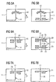
- FIGS. 3a and 3b show somewhat modified conductor track structures 12, 13 on the front and on the back.
- the roof capacity forming second trace structure parts 15 ', 21' is not mirror-symmetrical to the main extension direction R executed. Due to the asymmetry of two reflection points at the ends of the trace structure parts 15 ', 21' therefore creates a superposition of two waves with slightly different phase angles. Although this reduces On the one hand the quality of the antenna, but on the other hand leads to a desired increase in bandwidth.
- the symmetrical case according to Figures 2a and 2b arise at each of the two ends waves with the same phase, so that these ends act as a common point of resonance. The increase in bandwidth is especially in mobile phones important in which it is the hand of the user resonances on the antenna comes.
- FIGs 4a and 4b show a further embodiment an antenna 10 according to the invention.
- the first printed conductor structure parts 14, 20 respectively correspond to the Embodiments in Figures 2a to 3b. Is changed however, the shape of the second wiring pattern parts 16, 22.
- the second wiring pattern parts 16, 22 extend in each case on both sides from the end of the first printed conductor structure part 14, 20 away meandering in a substantially transverse to the first interconnect structure part 14, 20 extending Main direction. That is, the "T-bar" is here even meandering executed.
- This form of second trace structure parts 16, 22 is in both the front trace structure 12 as well as the rear Track structure 13 is carried out in this way.
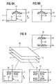
- FIG. 5a shows the front side of another one Embodiment.
- the carrier 11 is cut out accordingly.
- the backside trace structure 13 is again adapted to the front trace structure 12, that is, on the upper side corresponds to the second conductor structure part 22 'of the second conductor pattern part 16' of the front Printed Circuit Structure 12.
- the Lower Second Printed Circuit Structure Part 21 is similar to the second trace structure part 21 executed according to the antenna of Figure 2b.
- FIGS. 6a and 6b An embodiment is shown in FIGS. 6a and 6b. in which the front conductor track structure 12 exactly the front Conductor 12 corresponds to the antenna of Figure 2a.
- the back conductor pattern 20 In the back conductor pattern 20, however, are the second wiring pattern parts 23 each constructed so that a meandering section 24 to the opposite end of the first conductor pattern part 20 extends and another meandering portion 25 extends outwardly. This increases the capacity additionally.
- FIGS. 7a to 8b show two different exemplary embodiments of antennas, where the rear trace structure 13 each only at one end of the first conductor track structure part 20 a second printed conductor structure part 21 ', 22 ', that is, the "vertical" part of the structure 13 is only capacitively loaded on one side.
- the fronts of the Antennas according to FIGS. 7a and 8a correspond to the antennas according to the figures 3a and 5a.
- Such one-sided capacitive Loads of the vertical element are also possible and can be useful under certain conditions. she lead, however, that the maximum current is no longer in the Center of the first conductor pattern part 20 is located.
- To one good overcoupling to the vertical conductor section 17 of the first wiring pattern part 14 of the front To obtain wiring pattern 12 is therefore the embodiment with a bilateral capacitive loading of the first Track structure part 20 on the backside trace structure 13 preferred.
- FIG. 9 shows a further multiband antenna which is suitable for three different frequency bands is provided. Accordingly The antenna is superimposed in three levels Structures 12, 13, 26.
- the first interconnect structure 12 and the second conductive pattern 13 located in the middle correspond here to the conductor track structures 12, 13 on the Front and back of the antenna according to Figures 2a and 2 B.
- the levels are arbitrarily interchangeable.
- the contact pad by the above-or underlying levels in a suitable manner to the outside be plated through.
- the Antenna according to the invention in a variety of forms executable and thus to a variety of housing and the available space adaptable.
- Prototypes by soldering or removing traces are easily changeable. Because the exact adaptation of the antenna with respect to the different resonances and the impedance of very many external, badly influenced parameters, for example, the shape of the housing, the shield cover, the depends on the motherboard components etc., the optimal structure is extremely difficult or not at all predictable. It is therefore usually in the Development of such antennas several experiments with different Prototypes required to run the device for each device find optimal antenna shape or structure, so that with The antennas according to the invention also benefits from a Reduction of development times and costs can be achieved can.
Description
Die Erfindung betrifft eine Antenne für ein Kommunikationsendgerät mit einer auf oder in einem Träger aufgebrachten Leiterbahnstruktur sowie ein Kommunikationsendgerät mit einer solchen Antenne.The invention relates to an antenna for a communication terminal with an applied on or in a carrier Conductor structure and a communication terminal with a such antenna.
Mit der fortschreitenden Miniaturisierung von mobilen Kommunikationsendgeräten, insbesondere Mobiltelefonen, werden in Zukunft von den Abmessungen her immer kleinere Antennen benötigt. Im Bereich der Mobiltelefone werden daher in letzter Zeit überwiegend sogenannte "Stummelantennen" eingesetzt, die lediglich ein kurzes Stück aus dem Gehäuse hinausragen. Diese "Stummelantennen" haben den Nachteil, daß sie mechanisch empfindlich sind und abbrechen können. Darüber hinaus sollen auch aus Design-Gründen die Antennen möglichst vollständig optisch in dem miniaturisierten Gehäuse verschwinden. Eine Möglichkeit, Antennen vollständig zu integrieren, besteht darin, Antennen der eingangs genannten Art mit einer in bzw. auf einem Träger aufgebrachten Leiterbahnstruktur, beispielsweise sogenannte "PCB-Antennen" (Printed Circuit Board - Antennen), zu verwenden.With the progressive miniaturization of mobile Communication terminals, in particular mobile phones are in the future smaller dimensions due to their size needed. In the field of mobile phones are therefore in Most recently, so-called "stub antennas" were used, the only a short distance from the case protrude. These "stub antennas" have the disadvantage that they are mechanically sensitive and can break off. About that In addition, for design reasons, the antennas as possible completely optically in the miniaturized housing disappear. One way to fully connect antennas integrate, consists of antennas of the aforementioned Type with a conductor track structure applied in or on a carrier, for example, so-called "PCB antennas" (Printed Circuit Board - Antennas).
Eine solche integrierte Antenne muß in der Lage sein, die gesamte Bandbreite des jeweiligen Funkkanals abzudecken. Beispielsweise wird bei dem sogenannten GSM 900 MHz-Band im Bereich von 880 bis 915 MHz gesendet und im Bereich von 925 bis 960 MHz empfangen, so daß die Antenne den Bereich von 880 bis 960 MHz gut abdecken muß. Hinzu kommt insbesondere bei Mobiltelefonen das Problem, daß es während der Sprechzeit zu unterschiedlich starken Resonanzverschiebungen der Antenne kommen kann, die durch die verschiedenen Lagen der Mobilfunkgeräte in der Hand des Nutzers hervorgerufen werden. Diese Verschiebung der Resonanzfrequenz muß dementsprechend dadurch ausgeglichen werden, daß die Antenne noch breitbandiger als das benötigte Frequenzband ist, so daß auch bei einer Verschiebung der Resonanzfrequenz im gesamten Band gearbeitet werden kann. Breitbandige Antennen ergeben sich aber üblicherweise dann, wenn sie geometrisch groß sind, was der Zielsetzung nach einer miniaturisierten Antenne entgegenläuft. Eine ideale Antenne hätte beispielsweise eine wirksame Länge von einem Vielfachen einer viertel Wellenlänge (λ/4) der Mittenfrequenz, im Falle des GSM 900 MHz-Band von 920 MHz. Diese Länge ist aber durch die Platzvorgaben im Gehäuse oft nicht erreichbar.Such an integrated antenna must be able to cover the entire bandwidth of the respective radio channel. For example, in the so-called GSM 900 MHz band in the Range from 880 to 915 MHz and in the range of 925 to 960 MHz, so that the antenna covers the range of 880 must cover well up to 960 MHz. In addition, especially at Mobile phones have the problem that it is during talk time too different strong resonance shifts of the antenna can come through the different layers of mobile devices in the user's hand. These Displacement of the resonance frequency must accordingly be compensated that the antenna is still broadband than the required frequency band is, so that synonymous with a Shifting of the resonant frequency worked throughout the band can be. However, broadband antennas usually arise then, if they are geometrically big, what the Objective for a miniaturized antenna runs counter. For example, an ideal antenna would have an effective antenna Length of a multiple of a quarter wavelength (λ / 4) the center frequency, in the case of the GSM 900 MHz band of 920 MHz. This length is due to the space in the housing often not available.
Aus der Druckschrift EP 0 954 054 A1 ist eine kapazitive Kopplung einer Faltantenne mit einer Peitschenantenne bekannt.From the document EP 0 954 054 A1 is a capacitive Coupling a folding antenna with a whip antenna known.
Die Druckschrift WO 98/38694 offenbart eine Resonanzantenne für einen Funkkanal.Document WO 98/38694 discloses a resonant antenna for a radio channel.
Aus der Druckschrift US 5,809,433 ist eine unter einer Tastatur anbringbare Antennenvorrichtung bekannt. Die Antennenvorrichtung weist einen ersten Antennenteil und einen in der selben Ebene obehalb des ersten Antennenteils angeordneten zweiten Antennenteil auf.From the document US 5,809,433 is one under a Keyboard attachable antenna device known. The Antenna device has a first antenna part and a in the same plane above the first antenna part arranged on the second antenna part.
Es ist Aufgabe der vorliegenden Erfindung, eine Antenne mit relativ großer Bandbreite zu schaffen, die billig und reproduzierbar herstellbar ist.It is an object of the present invention to provide an antenna to create relatively large bandwidth, which is cheap and reproducible can be produced.
Diese Aufgabe wird durch die Antenne mit den Merkmalen des unabhängigen Anspruchs 1 gelöst.This task is performed by the antenna with the characteristics of independent claim 1 solved.
Eine erfindungsgemäße kapazitive Belastung am Ende des ersten Leiterbahnstruktur-Teils führt zu einer Verbesserung der Stromverteilung der Antenne. Die kapazitive Belastung bewirkt hierbei eine virtuelle Verlängerung der gesamten Antenne, so daß die Abweichung der wirksamen Länge von der idealen Länge durch die kapazitive Belastung kompensiert werden kann. Die "Höhe" der Antenne wird dabei nicht vergrößert, da sich die Umwegleitungen der kapazitiven Last überwiegend quer zur Höhe erstrecken.A capacitive load according to the invention at the end of the first Track structure part leads to an improvement of Power distribution of the antenna. The capacitive load causes this is a virtual extension of the entire antenna, so that the deviation of the effective length from the ideal length can be compensated by the capacitive load. The "Height" of the antenna is not increased, since the Detour lines of the capacitive load predominantly across the height extend.
Die kapazitive Belastung hat somit eine ähnliche Wirkung, wie die aus dem Bereich des "normalen" Rundfunkantennenbaus bekannten Dachkapazitäten, die am oberen Ende von auf Gebäuden etc. aufgestellten, vertikalen Monopol-Stabantennen angeordnet sind, wobei hier jedoch zusätzlich zu beachten ist, daß aufgrund der geringen geometrischen Abmessungen und der Nähe zum Schirmdeckel, der Platine, dem Akkupack oder anderen Teilen des Geräts unvermeidliche Kapazitäten gegen die Masse des Geräts auftreten und es außerdem zu den besagten Verstimmungen durch die Hand des Benutzers kommt.The capacitive load thus has a similar effect as those from the field of "normal" radio antenna construction well-known roof capacities, which at the upper end of on Buildings, etc., erected vertical monopole rod antennas are arranged, but in addition to note here is that due to the small geometric dimensions and close to the shield cover, the board, the battery pack or other parts of the device against unavoidable capacity the mass of the device will occur and it will also cause the said upsets come through the user's hand.
Die beiden Leiterbahnstruktur-Teile können im Prinzip relativ beliebig an die technischen Vorgaben sowie die zur Verfügung stehenden räumlichen Abmessungen angepaßt sein. Der zweite Leiterbahnstruktur-Teil sollte sich jedoch im wesentlichen quer zum ersten Leiterbahnstruktur-Teil erstrecken. Der erste Leiterbahnstruktur-Teil entspricht dabei quasi der Stabantenne mit einer Haupterstreckungsrichtung, welche beim "normalen" Rundfunkantennenbau die vertikale Richtung darstellt; der zweite Leiterbahnstruktur-Teil entspricht der horizontalen Dachkapazität. Vorzugsweise weist der erste Leiterbahnstruktur-Teil hierbei eine langgestreckte Leiterbahn auf, die sich endseitig zur Bildung des zweiten Leiterbahnstruktur-Teils aufgabelt.The two conductor track structure parts can in principle be relative arbitrary to the technical specifications as well as the available be adapted to the existing spatial dimensions. The second However, trace element part should be substantially extend transversely to the first printed conductor structure part. The first Conductor structure part corresponds to the rod antenna with a main extension direction, which at "normal" broadcast antenna construction the vertical direction represents; the second trace structure part corresponds to the horizontal roof capacity. Preferably, the first Conductor structure part in this case an elongated Trace on, which ends up forming the second Ladder Structure Part forks.
Der zweite Leiterbahnstruktur-Teil weist bevorzugt einen sich unter Bildung eines T-Balkens am Ende des ersten Leiterbahnstruktur-Teils erstreckenden Leiterbahnabschnitt auf. Im einfachsten Fall besteht der zweite Leiterbahnstruktur-Teil lediglich aus diesem einen Leiterbahnabschnitt, so daß insgesamt die Leiterbahnstruktur eine einfache T-Form aufweist. Insbesondere kann aber, um die Dachkapazität genau anzupassen, der zweite Leiterbahnstruktur-Teil auch mäanderförmig oder auf bestimmten Teilabschnitten mäanderförmig ausgeführt sein. Verschiedene spezielle Ausführungsbeispiele werden noch anhand beigefügter Zeichnungen beschrieben.The second interconnect structure part preferably has one forming a T-bar at the end of the first trace structure part extending conductor track section. in the The simplest case is the second interconnect structure part only from this one track section, so that in total the conductor track structure has a simple T-shape. In particular, in order to adapt the roof capacity precisely, the second interconnect structure part also meandering or meandered on certain sections be. Various specific embodiments are still described with reference to accompanying drawings.
Je nach Bedarf kann der zweite Leiterbahnstruktur-Teil bezüglich des ersten Leiterbahnstruktur-Teils symmetrisch oder asymmetrisch aufgebaut sein. Im Gegensatz zu einem symmetrischen Aufbau führt eine Asymmetrie im zweiten Leiterbahnstruktur-Teil dazu, daß aufgrund der zwei unterschiedlich zum ersten Leiterbahnstruktur-Teil beabstandeten Reflektionsstellen an den Enden der Dachkapazität eine Überlagerung zweier Wellen mit leicht unterschiedlicher Phasenlage auftritt. Dies führt einerseits zu einer Verringerung der Güte der Antenne, andererseits aber zu einer wünschenswerten Vergrößerung der Bandbreite.Depending on requirements, the second conductor structure part symmetrical with respect to the first trace structure part or asymmetric. Unlike one Symmetrical structure performs an asymmetry in the second Track structure part to that due to the two different from the first interconnect structure part spaced reflection points at the ends of the roof capacity a superposition of two waves with slightly different Phase occurs. This leads on the one hand a reduction in the quality of the antenna, but on the other hand too a desirable increase in bandwidth.
Die Leiterbahnstruktur kann so ausgeführt sein, daß der erste Leiterbahnstruktur-Teil in dem dem zweiten Leiterbahnstruktur-Teil gegenüberliegenden Endbereich ein Anschlußelement, beispielsweise einen Kontakt-Pad aufweist, mit dem über eine Kontaktfeder ein Anschluß an die Sende-/Empfangseinrichtung des Kommunikationsendgeräts erfolgt. Dieser Anschlußpunkt entspricht dem Fußpunkt einer vertikalen Antenne mit Dachkapazität. Alternativ ist es auch möglich, daß der erste Leiterbahnstruktur-Teil an beiden Enden mit einem zweiten Leiterbahnstruktur-Teil kapazitiv belastet ist. In diesem Fall wird die Leistung in die Antenne in den ersten Leiterbahnstruktur-Teil kapazitiv bzw. induktiv eingekoppelt.The conductor track structure can be designed so that the first Conductor structure part in the second conductor structure part opposite end portion of a connecting element, For example, has a contact pad, with the over a Contact spring a connection to the transmitting / receiving device the communication terminal takes place. This connection point corresponds to the base of a vertical antenna with Top capacity. Alternatively, it is also possible that the first Conductor structure part at both ends with a second Conductor structure part is loaded capacitively. In this Case, the power in the antenna in the first Conductor structure part coupled capacitively or inductively.
Damit die Antenne als sogenannte "Multiband-Antenne" in verschiedenen Frequenzbereichen arbeiten kann, weist sie vorzugsweise einen ersten Antennenteil mit einer ersten Leiterbahnstruktur und in einer im wesentlichen parallel zu der ersten Leiterbahnstruktur liegenden Ebene einen weiteren Antennenteil mit einer weiteren Leiterbahnstruktur auf, wodurch die Antenne auf einen gewünschten weiteren Funkkanal, d. h. auf eine zweite Resonanz, abgestimmt wird. Die weitere Leiterbahnstruktur ist hierbei kapazitiv bzw. induktiv mit der ersten Leiterbahnstruktur gekoppelt. Im einfachsten Fall handelt es sich bei dem Träger um eine Platine, welche auf der einen Oberfläche die erste Leiterbahnstruktur und auf der gegenüberliegenden Oberfläche eine zweite Leiterbahnstruktur aufweist. Selbstverständlich ist es aber auch möglich, daß es sich um eine Art Multilayer-Platine handelt, die in verschiedensten Ebenen noch weitere Leiterbahnstrukturen aufweist, wodurch die Antenne nicht nur in zwei, sondern auch in mehreren Resonanzbereichen arbeiten kann. So that the antenna as so-called "multi-band antenna" in can work in different frequency ranges, she points out preferably a first antenna part with a first Conductor structure and in a substantially parallel to the first conductor track structure lying another level Antenna part with a further interconnect structure, whereby the antenna is tuned to a desired further radio channel, d. H. to a second resonance, is tuned. The others Conductor structure here is capacitive or inductive with coupled to the first interconnect structure. In the simplest case it is the carrier to a board, which on one surface the first conductor track structure and on the opposite surface of a second interconnect structure having. Of course, it is also possible that it is a kind of multilayer board, which in At various levels even more interconnect structures which makes the antenna not only in two but also can work in several resonance ranges.
Bei einer bevorzugten Ausführungsform weist der erste Leiterbahnstruktur-Teil der ersten Leiterbahnstruktur an einem Ende das Anschlußelement, zum Beispiel das Kontakt-Pad, auf, und der erste Leiterbahnstruktur-Teil der weiteren Leiterbahnstruktur ist an beiden Enden durch einen zweiten Leiterbahnstruktur-Teil kapazitiv belastet. Um eine optimale Überkopplung zwischen der zweiten Leiterbahnstruktur und der ersten Leiterbahnstruktur zu gewährleisten, sind die Leiterbahnstrukturen bzw. auch jede weitere Leiterbahnstruktur bzgl. der Haupterstreckungsrichtung des jeweils ersten Leiterbahnstruktur-Teils parallel zueinander orientiert, das heißt, die "vertikalen" Antennenteile liegen jeweils im wesentlichen parallel, da auf diesem Stück die Überkopplung hauptsächlich stattfindet.In a preferred embodiment, the first Conductor structure part of the first interconnect structure one end the connection element, for example the contact pad, on, and the first trace structure part of the other Track structure is at both ends by a second Conductor structure part capacitively loaded. To be optimal Overcoupling between the second interconnect structure and the to ensure the first interconnect structure are the Conductor structures or any other Conductor structure with respect to the main extension direction of the each first interconnect structure part parallel to each other oriented, that is, the "vertical" antenna parts lie each substantially parallel, since on this piece the Overcoupling mainly takes place.
Die Erfindung wird im folgenden unter Hinweis auf die beigefügten
Zeichnungen anhand von Ausführungsbeispielen näher
erläutert. Die dargestellten Merkmale können nicht nur in den
genannten Kombinationen, sondern auch einzeln oder in anderen
Kombinationen erfindungswesentlich sein. Es zeigen:
Da der Haupteinsatzbereich der erfindungsgemäßen Antennen 10
im Bereich von Mobiltelefonen 1 liegt und hier auch
insbesondere wegen der Probleme der Abdeckung der Antenne mit
der Hand des Benutzers besonders große Vorteile bietet, wird
in den folgenden Ausführungsbeispielen von Antennen für
Mobiltelefone ausgegangen. Es wird aber noch einmal darauf
hingewiesen, daß der Einsatz solcher Antennen selbstverständlich
nicht auf Mobiltelefone beschränkt ist.Since the main application area of the
Figur 1 zeigt ein solches typisches Mobiltelefon 1 mit einem
Gehäuse 2 und einer integrierten erfindungsgemäßen Antenne
10. Die weiteren Komponenten des Mobiltelefons 1 sind nur
teilweise und schematisch dargestellt. Das Mobiltelefon weist
zum einen eine Hauptplatine 3 auf, auf der im oberen Bereich
die Hörkapsel 6 und darunter das Display 5 angeordnet sind.
Unterhalb des Displays 5 befindet sich die Tastatur (nicht
dargestellt). Auf der Rückseite der Hauptplatine 3 ist unter
anderem der Akkupack 4 angeordnet. Die Hauptplatine 3 und der
Akkupack 4 sind üblicherweise durch einen Schirmdeckel 8 aus
elektrisch leitendem Material abgeschirmt. In dem oberen
freien Raum des Gehäuses hinter der Hörkapsel 6 zwischen der
Rückseite der Hauptplatine 3 oberhalb des Akkupacks 4
befindet sich ein freier Raum 9, in dem die Antenne 10
angeordnet ist.Figure 1 shows such a typical mobile phone 1 with a
Diese Antenne 10 besteht im wesentlichen aus einem Träger 11
und einer auf der zur Hauptplatine 3 weisenden Vorderseite
des Trägers 11 befindlichen ersten Leiterbahnstruktur 12 und
einer auf der Rückseite angeordneten zweiten Leiterbahnstruktur
13.This
In einem besonders einfachen und kostengünstig herstellbaren
Fall besteht die Antenne 10 im wesentlichen aus einer
doppelseitigen Platine, auf welcher beiseitig durch ein
übliches Ätzverfahren die Leiterbahnstruktur 12, 13 erzeugt
wurde. Selbstverständlich können die Leiterbahnstrukturen auf
beiden Seiten auch aufgedruckt oder in einer anderen
geeigneten Weise auf einem geeigneten Träger 11 aufgebracht
sein.In a particularly simple and inexpensive to produce
Case, the
In Figur 2a ist die erste Leiterbahnstruktur 12 auf der
Vorderseite einer Antenne gemäß einem ersten
Ausführungsbeispiel dargestellt.In Figure 2a, the
Die erste Leiterbahnstruktur 12 besteht hier aus einem ersten
Leiterbahnstruktur-Teil 14, welches wiederum aus einem
bezüglich der Längsachse des Mobiltelefons 1 parallelen,
"vertikalen" Leiterbahnabschnitt 17 und am unteren Ende einem
"horizontalen" Leiterbahnabschnitt 18 besteht.The first printed
Der erste, "vertikale" Leiterbahnabschnitt 17 weist am oberen
Ende als Dachkapazität den zweiten Leiterbahnstruktur-Teil 15
auf. Der zweite, "horizontale" Leiterbahnabschnitt 18 des
ersten Leiterbahnstruktur-Teils 14 dient dazu, um das untere
Ende des ersten Leiterbahnabschnitts 17 mit dem Kontakt-Pad
19 zu verbinden, welcher in der in der Draufsicht linken
unteren Ecke des Trägers 11 angeordnet ist. Über diesen
Kontakt-Pad 19 ist die Antenne 1 über eine Kontaktfeder 7 mit
einer entsprechenden Zuleitung auf der Hauptplatine 3 zu
einer Sende-/Empfangseinheit (nicht dargestellt) verbunden
(siehe Figur 1). Die Kontaktfeder 7 überbrückt im
vorliegenden Ausführungsbeispiel einen Abstand a von ca. 6
bis 12 mm.The first, "vertical"
In sämtlichen in den Figuren gezeigten Ausführungsbeispielen
ist der Kontakt-Pad 19 an derselben Stelle dargestellt. Diese
Position ist jedoch lediglich durch den Aufbau des jeweiligen
Mobiltelefons 1 bedingt. Der Kontakt-Pad kann selbstverständlich
auch an einer beliebigen anderen Stelle, beispielsweise
in der Mitte unten oder in der rechten unteren Ecke des
Trägers 11 angeordnet sein.In all embodiments shown in the figures
the
Der gesamte erste Leiterbahnstruktur-Teil 14 bildet hierbei,
ausgehend von der Auskopplungsstelle zur Sende-/Empfangseinheit,
als sogenannter "Fußpunkt", bis zum oberen Ende,
eine Monopol-Antenne, die quasi der im Rundfunkantennenbau
bekannten "Stabantenne" entspricht. Endseitig ist diese
"Stabantenne" durch den zweiten Leiterbahnstruktur-Teil 15
kapazitiv belastet.The entire first
Zur Bildung dieser "Dachkapazität" 15 ist der Leiterbahnabschnitt
17 endseitig aufgegabelt, das heißt, der zweite
Leiterbahnstruktur-Teil 15 weist einen Leiterbahnabschnitt 29
auf, der sich wie ein T-Balken am Ende des Leiterbahnabschnitts
17 des ersten Leiterbahnstruktur-Teils 14 erstreckt.To form this "roofing capacity" 15 is the
Jeweils an beiden Enden dieses den T-Balken bildenden
Leiterbahnabschnitts 29 erstrecken sich in einer parallel zur
Haupterstreckungsrichtung R des ersten Leiterbahnstruktur-Teils
14, d. h. in Richtung des Leiterbahnabschnitts 17,
mäanderförmig verlaufende weitere Leiterbahnabschnitte 24.
Diese mäanderförmigen Leiterbahnabschnitte 24 bestehen
wiederum aus geraden, senkrecht und parallel zum
Leiterbahnabschnitt 17 orientierten, einzelnen Abschnitten.
Im gezeigten Ausführungsbeispiel erstrecken sie sich von den
Enden des T-Balkens aus nach unten, d. h. in Richtung des
vertikalen Leiterbahnabschnitts 17 des ersten Leiterbahnstruktur-Teils
14 entgegen der Haupterstreckungsrichtung R.
Selbstverständlich könnten sie sich auch in Richtung der
Haupterstreckungsrichtung R, d. h. nach oben, erstrecken.
Durch die genaue Form des Mäanders läßt sich insbesondere die
räumliche Ausdehnung im Verhältnis zur Antennenlänge verändern
und dadurch die Kapazität zum Schirmdeckel 8 und zu
anderen Komponenten des Mobiltelefons 1 entsprechend einstellen,
um die Antenne an die gewünschte Resonanzfrequenz
anzupassen.In each case at both ends of this the T-bar forming
Der zweite Leiterbahnstruktur-Teil 15 ist hier spiegelsymmetrisch
zum ersten Leiterbahnabschnitt 17 des ersten
Leiterbahnstruktur-Teils 14 ausgeführt. The second printed
Auf der Rückseite des Trägers 11 befindet sich ein weiterer
Antennenteil mit einer weiteren Leiterbahnstruktur 13. Diese
Leiterbahnstruktur 13 ist zu der Leiterbahnstruktur 14 auf
der Vorderseite sehr ähnlich aufgebaut. Der erste
Leiterbahnstruktur-Teil 20 dieser zweiten Leiterbahnstruktur
13 entspricht hierbei dem vertikalen Leiterbahnabschnitt 17
des ersten Leiterbahnstruktur-Teils 14 der Leiterbahnstruktur
12 auf der Vorderseite. Dieser erste Leiterbahnstruktur-Teil
20 ist jedoch an beiden Enden mit einem weiteren, als
kapazitive Belastung dienenden Leiterbahnstruktur-Teil 21
versehen, welcher hier genau dem zweiten Leiterbahnstruktur-Teil
15 auf der Vorderseite entspricht.On the back of the
Im vorliegenden Ausführungsbeispiel ist der Antennenteil auf
der Vorderseite, d. h. die Leiterbahnstruktur 12, so ausgeführt,
daß eine Resonanzfrequenz der Antenne im Bereich des
900 MHz-Bandes des GSM-Systems liegt, wobei selbstverständlich
die Einflüsse durch die rückseitige Struktur 13
berücksichtigt sind. Die hintere Struktur 13 koppelt
kapazitiv bzw. induktiv auf die vordere Struktur 12 über bzw.
umgekehrt. Die hintere Struktur 13 ist so ausgeführt, daß
eine zweite Resonanz bei dem 1800 MHz-Band des GSM-Systems
liegt. Das heißt, die Gesamtstruktur ist so ausgebildet, daß
die ansonsten bei einer ¾ λ entsprechenden Frequenz von ca.
2700 MHz liegenden nächst höhere Resonanzstelle, welche einen
guten Realteil aufweist, auf ca. 1800 MHz heruntergezogen
wird. Die genaue Abstimmung der Resonanz erfolgt im
wesentlichen durch die Leiterbahnstrukturen 12, 13 auf der
Vorder- und Rückseite. Neben der jeweiligen speziellen
Ausformung der Strukturen 12, 13 haben aber selbstverständlich
auch die Dicke des Trägers 11, und damit der
Abstand der beiden Leiterbahnstrukturen 12, 13 zueinander,
sowie die Materialkonstanten, beispielsweise die
Dielektrizitätskonstante, des Trägermaterials Auswirkungen
auf die Resonanzabstimmung der gesamten Antenne 10 und müssen
entsprechend berücksichtigt werden, bzw. können geeignet
gewählt werden. In the present embodiment, the antenna part is on
the front, d. H. the
Insbesondere können auch die Breiten der Leiterbahnen des ersten Leiterbahnstrukturteils und der kapazitiven Belastungen variiert werden. Die Leiterbahnbreite hat u. a. starken Einfluß auf die Güte der Antenne und folglich auf die Resonanzbandbreite. Dies gilt auch für einfache Antennen mit nur einem Antennenteil.In particular, the widths of the tracks of the first conductor structure part and the capacitive Loads are varied. The track width has u. a. strong influence on the quality of the antenna and consequently on the Resonance bandwidth. This also applies to simple antennas with only one antenna part.
Die Figuren 3a und 3b zeigen etwas veränderte Leiterbahnstrukturen
12, 13 auf der Vorder- und auf der Rückseite. Im
Gegensatz zu der Antenne gemäß den Figuren 2a und 2b sind
hier die Dachkapazität bildenden zweiten Leiterbahnstruktur-Teile
15', 21' nicht spiegelsymmetrisch zur Haupterstreckungsrichtung
R ausgeführt. Durch die Asymmetrie der
zwei Reflektionsstellen an den Enden der Leiterbahnstruktur-Teile
15', 21' entsteht daher eine Überlagerung zweier Wellen
mit leicht unterschiedlicher Phasenlage. Dies verringert zwar
einerseits die Güte der Antenne, führt aber andererseits zu
einer gewünschten Vergrößerung der Bandbreite. Im
symmetrischen Fall gemäß den Figuren 2a und 2b entstehen an
den beiden Enden jeweils Wellen mit gleicher Phasenlage, so
daß diese Enden wie eine gemeinsame Resonanzstelle wirken.
Die Vergrößerung der Bandbreite ist insbesondere bei Mobiltelefonen
wichtig, bei denen es durch die Hand des Benutzers
zu Resonanzverstimmungen an der Antenne kommt.FIGS. 3a and 3b show somewhat modified
Die Figuren 4a und 4b zeigen ein weiteres Ausführungsbeispiel
einer erfindungsgemäßen Antenne 10. Die ersten Leiterbahnstruktur-Teile
14, 20 entsprechen hierbei jeweils den
Ausführungsformen in den Figuren 2a bis 3b. Verändert ist
jedoch die Form der zweiten Leiterbahnstruktur-Teile 16, 22.
Die zweiten Leiterbahnstruktur-Teile 16, 22 erstreckt sich
jeweils beidseitig vom Ende des ersten Leiterbahnstruktur-Teils
14, 20 weg mäanderförmig in einer im wesentlichen quer
zum ersten Leiterbahnstruktur-Teil 14, 20 verlaufenden
Haupterstreckungsrichtung. Das heißt, der "T-Balken" ist
hierbei selber mäanderförmig ausgeführt. Diese Form der
zweiten Leiterbahnstruktur-Teile 16, 22 ist sowohl bei der
vorderen Leiterbahnstruktur 12 als auch bei der hinteren
Leiterbahnstruktur 13 so ausgeführt.Figures 4a and 4b show a further embodiment
an
Die Figur 5a zeigt die Vorderseite eines weiteren
Ausführungsbeispiels. Hierbei ist lediglich im Gegensatz zu
der Form gemäß Figur 4a der zweite Leiterbahnstruktur-Teil
16' bogenförmig am Ende des ersten Leiterbahnstruktur-Teils
14 ausgeführt. Es liegt daher eine etwas erhöhte Kapazität
vor. Außerdem zeigt dieses Ausführungsbeispiel, daß durch
geeignete Wahl der Form des zweiten Leiterbahnstruktur-Teils
16' die Antenne auch an ein rundes Gehäuse angepaßt werden
kann. Hierzu wird dementsprechend der Träger 11 ausgeschnitten.
Die rückseitige Leiterbahnstruktur 13 ist wiederum
an die vordere Leiterbahnstruktur 12 angepaßt, das heißt, auf
der oberen Seite entspricht der zweite Leiterbahnstruktur-Teil
22' dem zweiten Leiterbahnstruktur-Teil 16' der vorderen
Leiterbahnstruktur 12. Der untere zweite Leiterbahnstruktur-Teil
21 ist dagegen ähnlich dem zweiten Leiterbahnstruktur-Teil
21 gemäß der Antenne nach Figur 2b ausgeführt.FIG. 5a shows the front side of another one
Embodiment. This is just in contrast to
the shape according to Figure 4a, the second interconnect structure part
16 'arcuate at the end of the first
In den Figuren 6a und 6b ist ein Ausführungsbeispiel gezeigt,
bei dem die vordere Leiterbahnstruktur 12 genau der vorderen
Leiterbahnstruktur 12 der Antenne nach Figur 2a entspricht.
Bei der rückseitigen Leiterbahnstruktur 20 sind jedoch die
zweiten Leiterbahnstruktur-Teile 23 jeweils so aufgebaut, daß
sich ein Mäanderabschnitt 24 zum gegenüberliegenden Ende des
ersten Leiterbahnstruktur-Teils 20 erstreckt und ein weiterer
mäanderförmiger Abschnitt 25 nach außen erstreckt. Dies
erhöht die Kapazität zusätzlich.An embodiment is shown in FIGS. 6a and 6b.
in which the front
Die Figuren 7a bis 8b zeigen zwei verschiedene Ausführungsbeispiele
von Antennen, bei denen die hintere Leiterbahnstruktur
13 jeweils nur an einem Ende des ersten Leiterbahnstruktur-Teils
20 einen zweiten Leiterbahnstruktur-Teil 21',
22' aufweist, das heißt, der "vertikale" Teil der Struktur 13
ist nur einseitig kapazitiv belastet. Die Vorderseiten der
Antennen gemäß den Figuren 7a und 8a entsprechen den Antennen
gemäß den Figuren 3a und 5a. Derartige einseitige kapazitive
Belastungen des vertikalen Elements sind ebenfalls möglich
und können unter bestimmten Bedingungen sinnvoll sein. Sie
führen jedoch dazu, daß das Strommaximum nicht mehr in der
Mitte des ersten Leiterbahnstruktur-Teils 20 liegt. Um eine
gute Überkopplung zum vertikalen Leiterbahnabschnitt 17 des
ersten Leiterbahnstruktur-Teils 14 der vorderen
Leiterbahnstruktur 12 zu erhalten, ist daher die Ausführungsform
mit einer beidseitigen kapazitiven Belastung des ersten
Leiterbahnstruktur-Teils 20 auf der rückseitigen Leiterbahnstruktur
13 bevorzugt.FIGS. 7a to 8b show two different exemplary embodiments
of antennas, where the
Figur 9 zeigt eine weitere Multiband-Antenne, die für drei
verschiedene Frequenzbänder vorgesehen ist. Dementsprechend
weist die Antenne in drei Ebenen übereinanderliegende
Strukturen 12, 13, 26 auf. Die erste Leiterbahnstruktur 12
und die in der Mitte liegende zweite Leiterbahnstruktur 13
entsprechen hierbei den Leiterbahnstrukturen 12, 13 auf der
Vorder- und Rückseite der Antenne gemäß den Figuren 2a und
2b. Darüber befindet sich eine dritte Leiterbahnstruktur 26,
welche entsprechend der rückseitigen Leiterbahnstruktur 20
der Antenne gemäß Figur 4b aufgebaut ist. Selbstverständlich
sind die Ebenen untereinander beliebig vertauschbar. Insbesondere
kann sich die Ebene mit der ersten Leiterbahnstruktur,
d. h. die Ebene mit dem Kontakt-Pad, auch in der Mitte,
zwischen den anderen Ebenen, befinden. In diesem Fall müssen
die über dem Kontakt-Pad liegenden Schichten des Trägers
entsprechende Aussparungen oder dergleichen aufweisen, um
eine Kontaktierung des Kontakt-Pads zu ermöglichen.
Alternativ kann der Kontakt-Pad auch durch die darüber- bzw.
darunterliegenden Ebenen in geeigneter Weise nach außen
durchkontaktiert sein.FIG. 9 shows a further multiband antenna which is suitable for three
different frequency bands is provided. Accordingly
The antenna is superimposed in three
Wie die verschiedensten Ausführungsbeispiele zeigen, ist die erfindungsgemäße Antenne in den verschiedensten Formen ausführbar und somit an die verschiedensten Gehäuse und den zur Verfügung stehenden Platz anpaßbar. Es sind hiermit sehr kleine Antennen mit relativ großer Bandbreite in mehreren Frequenzbändern äußerst günstig herstellbar. Im Gegensatz zu den bisher für Dualband verwendeten Helix-Antennen haben sie darüber hinaus bei der Entwicklung den Vorteil, daß Prototypen durch Anlöten oder Entfernen von Leiterbahnteilen leicht veränderbar sind. Da die genaue Anpassung der Antenne bezüglich der verschiedenen Resonanzen und der Impedanz von sehr vielen äußeren, schlecht beeinflußbaren Parametern, beispielsweise der Form des Gehäuses, des Schirmdeckels, der auf der Hauptplatine befindlichen Komponenten etc. abhängt, ist die optimale Struktur nur äußerst schwer oder gar nicht vorab berechenbar. Es sind daher in der Regel bei der Entwicklung solcher Antennen mehrere Versuche mit unterschiedlichen Prototypen erforderlich, um für jedes Gerät die optimale Antennenform bzw. -struktur zu finden, so daß mit den erfindungsgemäßen Antennen auch Vorteile durch eine Reduzierung der Entwicklungszeiten und -kosten erzielt werden können.As the various embodiments show, is the Antenna according to the invention in a variety of forms executable and thus to a variety of housing and the available space adaptable. There are a lot here small antennas with relatively large bandwidth in several Frequency bands extremely cheap to produce. In contrast to they have so far used for dual band helix antennas In addition, in the development of the advantage that Prototypes by soldering or removing traces are easily changeable. Because the exact adaptation of the antenna with respect to the different resonances and the impedance of very many external, badly influenced parameters, for example, the shape of the housing, the shield cover, the depends on the motherboard components etc., the optimal structure is extremely difficult or not at all predictable. It is therefore usually in the Development of such antennas several experiments with different Prototypes required to run the device for each device find optimal antenna shape or structure, so that with The antennas according to the invention also benefits from a Reduction of development times and costs can be achieved can.
Claims (13)
- Multiband antenna (10) for a communications terminal (1) having a conductor track structure (12) which can be provided on and/or in a carrier (11), wherein the conductor track structure (12) has a first conductor track structure part (14) which is capacitively loaded at one end in order tune the antenna (10) to a desired radio channel by means of a second conductor track structure part (16, 16'), characterized in that the antenna has, for the purpose of tuning to a desired further radio channel, a first antenna part with a first conductor track structure (12) and a further antenna part in a plane which is located essentially in parallel opposite the first conductor track structure (12), which has a further conductor track structure (13) which is provided on and/or in the carrier (11) or on/in a further carrier, which conductor track structure (13) is capacitively and/or inductively coupled to the first conductor track structure (12), wherein the further conductor track structure (13) has a first conductor track structure part (20) which is capacitively loaded at the end in order to tune the antenna (10) to a desired radio channel by means of a further second conductive track structure part (22, 22'), wherein the second and the further second conductor track structure parts (16, 16', 22, 22') extend essentially transversely with respect to the particular first conductor track structure part (14, 20), and wherein the second and further second conductor track structure parts (16, 16', 22, 22') each extend on each side from the end of the particular first conductor track structure part (14, 20) in a meandering shape in a main extending direction which runs essentially transversely with respect to the first conductor track structure part (14, 20), or said second and further second conductor track structure parts (16, 16', 22, 22') extend in an arc shape at the end of the particular first conductor track structure part (14, 20).
- Antenna according to Claim 1, characterized in that the first conductor track structure part (14, 20, 27) has an elongated conductor track which forks at the end in order to form the second conductor track structure part (15, 15', 16, 16', 21, 21', 22, 22', 23, 28).
- Antenna according to Claim 1 or 2, characterized in that the second conductor track structure part (15, 15', 21, 21', 23) has a conductor track section (29) which extends while forming a T-shaped bar at the end of the first conductor track structure part (14, 20).
- Antenna according to Claim 3, characterized in that the second conductor track structure part (15, 15', 21, 21', 23) has further conductor track sections (24, 25) which run in a meandering fashion in a main extending direction which is oriented parallel to the first conductor track structure part (14, 20), at each of the two ends of the conductor track section (29) which form the T-shaped bar.
- Antenna according to one of the preceding claims, characterized in that the second conductor track structure part (15, 21, 28) is of symmetrical design with respect to the first conductor track structure part (14, 20, 27).
- Antenna according to one of Claims 1 to 4, characterized in that the second conductor track structure part (15', 21') is of asymmetrical design with respect to the first conductor track structure part (14, 20).
- Antenna according to one of the preceding claims, characterized in that the first conductor track structure part (14) has a connecting element (19) in the end region lying opposite the second conductor track structure part (15, 15', 16, 16').
- Antenna according to Claim 7, characterized in that the first conductor track structure part (14) has two conductor track sections (17, 18), wherein the first conductor track section (17) is capacitively loaded at one end by the second conductor track structure part (15, 15', 16, 16'), and the second conductor track section (18) connects the other end of the first conductor track section (17) to the connecting element (19).
- Antenna according to one of Claims 1 to 7, characterized in that the first conductor track structure part (20, 27) is capacitively loaded at both ends by a second conductor track structure part (21, 21', 22, 22'; 23, 28).
- Antenna according to one of the preceding claims, characterized in that the first conductor track structure part (14) of the first conductor track structure (12) has a connecting element (19) at one end, and the first conductor track structure part (20, 27) of the further conductor track structure (13, 26) has a second conductor track structure part (21, 21', 22, 22', 23, 28) as a capacitive load at both ends.
- Antenna according to one of the preceding claims, characterized in that a respective first conductor track structure part (14, 20, 27) of the first conductor track structure (12) and a respective first conductor track structure part (14, 20, 27) of the further conductor track structure (13, 26) are oriented essentially parallel to one another.
- Communications terminal (1) having an antenna according to one of Claims 1 to 11.
- Communications terminal according to Claim 12, characterized in that the terminal is a mobile phone (1) .
Applications Claiming Priority (3)
| Application Number | Priority Date | Filing Date | Title |
|---|---|---|---|
| DE19961488A DE19961488A1 (en) | 1999-12-20 | 1999-12-20 | Antenna for communications terminal has a relatively large bandwidth and can be manufactured cheaply and reproducibly |
| DE19961488 | 1999-12-20 | ||
| PCT/DE2000/004531 WO2001047056A2 (en) | 1999-12-20 | 2000-12-19 | Antenna for a communications terminal |
Publications (2)
| Publication Number | Publication Date |
|---|---|
| EP1250723A2 EP1250723A2 (en) | 2002-10-23 |
| EP1250723B1 true EP1250723B1 (en) | 2005-03-30 |
Family
ID=7933439
Family Applications (1)
| Application Number | Title | Priority Date | Filing Date |
|---|---|---|---|
| EP00990548A Expired - Lifetime EP1250723B1 (en) | 1999-12-20 | 2000-12-19 | Antenna for a communications terminal |
Country Status (5)
| Country | Link |
|---|---|
| US (1) | US6839040B2 (en) |
| EP (1) | EP1250723B1 (en) |
| CN (1) | CN1185762C (en) |
| DE (2) | DE19961488A1 (en) |
| WO (1) | WO2001047056A2 (en) |
Families Citing this family (25)
| Publication number | Priority date | Publication date | Assignee | Title |
|---|---|---|---|---|
| WO2001054225A1 (en) | 2000-01-19 | 2001-07-26 | Fractus, S.A. | Space-filling miniature antennas |
| EP1298807A1 (en) * | 2001-09-28 | 2003-04-02 | Siemens Aktiengesellschaft | Module for transmitting and/or receiving radio data |
| US9755314B2 (en) | 2001-10-16 | 2017-09-05 | Fractus S.A. | Loaded antenna |
| JP2003198410A (en) * | 2001-12-27 | 2003-07-11 | Matsushita Electric Ind Co Ltd | Antenna for communication terminal device |
| TW557604B (en) * | 2002-05-23 | 2003-10-11 | Realtek Semiconductor Corp | Printed antenna structure |
| EP1372213A1 (en) * | 2002-06-11 | 2003-12-17 | Industrial Technology Research Institute | Multi-frequency band antenna |
| JP2005531177A (en) | 2002-06-25 | 2005-10-13 | フラクトゥス・ソシエダッド・アノニマ | Multiband antenna for handheld terminal equipment |
| JP2006510321A (en) * | 2002-12-22 | 2006-03-23 | フラクタス・ソシエダッド・アノニマ | Multiband monopole antenna for mobile communication devices |
| WO2004070871A1 (en) * | 2003-02-10 | 2004-08-19 | Sony Ericsson Mobile Communications Ab | Combined speaker and antenna component |
| JP4010283B2 (en) * | 2003-06-17 | 2007-11-21 | ミツミ電機株式会社 | Antenna device |
| US6876332B1 (en) * | 2003-11-11 | 2005-04-05 | Realtek Semiconductor Corp. | Multiple-frequency antenna structure |
| DE10361634A1 (en) | 2003-12-30 | 2005-08-04 | Advanced Micro Devices, Inc., Sunnyvale | Powerful low-cost monopole antenna for radio applications |
| EP1709704A2 (en) * | 2004-01-30 | 2006-10-11 | Fractus, S.A. | Multi-band monopole antennas for mobile communications devices |
| JP2006340367A (en) * | 2005-06-02 | 2006-12-14 | Behavior Tech Computer Corp | Wireless transmission device with incorporated antenna and connector |
| KR100731600B1 (en) | 2005-12-26 | 2007-06-22 | (주)에이스안테나 | Embedded chip antenna of complementary radiator structure |
| JP3883565B1 (en) * | 2006-02-28 | 2007-02-21 | Tdk株式会社 | Chip antenna |
| US8738103B2 (en) | 2006-07-18 | 2014-05-27 | Fractus, S.A. | Multiple-body-configuration multimedia and smartphone multifunction wireless devices |
| EP1983467B1 (en) * | 2007-04-19 | 2013-03-13 | BALLUFF GmbH | Data carrier/transmission device and method for manufacturing it |
| FR2928037B1 (en) * | 2008-02-21 | 2010-03-26 | Composants Electr Soc D | ANTENNA FOR MOTOR VEHICLES, ESPECIALLY FOR THE RECEPTION OF TERRESTRIAL AND / OR SATELLITE RADIO SIGNALS. |
| KR101044994B1 (en) | 2008-06-20 | 2011-06-29 | 삼성전자주식회사 | Antenna apparatus of potable terminal |
| KR101133343B1 (en) * | 2011-01-04 | 2012-04-06 | 인천대학교 산학협력단 | Mimo(multi input multi output) antenna without phase variation |
| GB2493373A (en) * | 2011-08-03 | 2013-02-06 | Harada Ind Co Ltd | Antenna with a bent conductor for multiple frequency operation |
| US9786987B2 (en) * | 2012-09-14 | 2017-10-10 | Panasonic Intellectual Property Management Co., Ltd. | Small antenna apparatus operable in multiple frequency bands |
| US9711863B2 (en) | 2013-03-13 | 2017-07-18 | Microsoft Technology Licensing, Llc | Dual band WLAN coupled radiator antenna |
| CN112886232B (en) * | 2019-11-30 | 2022-10-11 | 华为技术有限公司 | Electronic device |
Citations (3)
| Publication number | Priority date | Publication date | Assignee | Title |
|---|---|---|---|---|
| WO1998038694A1 (en) * | 1997-02-25 | 1998-09-03 | Pates Technology Patentverwertungsgesellschaft Für Satelliten- Und Moderne Informationstechnologien Mbh | Resonant antenna |
| US5809433A (en) * | 1994-09-15 | 1998-09-15 | Motorola, Inc. | Multi-component antenna and method therefor |
| EP0986130A2 (en) * | 1998-09-08 | 2000-03-15 | Siemens Aktiengesellschaft | Antenna for wireless communication terminal device |
Family Cites Families (3)
| Publication number | Priority date | Publication date | Assignee | Title |
|---|---|---|---|---|
| EP0814536A3 (en) * | 1996-06-20 | 1999-10-13 | Kabushiki Kaisha Yokowo | Antenna and radio apparatus using same |
| EP0954054A1 (en) * | 1998-04-30 | 1999-11-03 | Kabushiki Kaisha Yokowo | Folded antenna |
| SE512524C2 (en) * | 1998-06-24 | 2000-03-27 | Allgon Ab | An antenna device, a method of producing an antenna device and a radio communication device including an antenna device |
-
1999
- 1999-12-20 DE DE19961488A patent/DE19961488A1/en not_active Withdrawn
-
2000
- 2000-12-19 CN CNB008172447A patent/CN1185762C/en not_active Expired - Fee Related
- 2000-12-19 EP EP00990548A patent/EP1250723B1/en not_active Expired - Lifetime
- 2000-12-19 DE DE50009947T patent/DE50009947D1/en not_active Expired - Lifetime
- 2000-12-19 WO PCT/DE2000/004531 patent/WO2001047056A2/en active IP Right Grant
- 2000-12-19 US US10/168,252 patent/US6839040B2/en not_active Expired - Fee Related
Patent Citations (3)
| Publication number | Priority date | Publication date | Assignee | Title |
|---|---|---|---|---|
| US5809433A (en) * | 1994-09-15 | 1998-09-15 | Motorola, Inc. | Multi-component antenna and method therefor |
| WO1998038694A1 (en) * | 1997-02-25 | 1998-09-03 | Pates Technology Patentverwertungsgesellschaft Für Satelliten- Und Moderne Informationstechnologien Mbh | Resonant antenna |
| EP0986130A2 (en) * | 1998-09-08 | 2000-03-15 | Siemens Aktiengesellschaft | Antenna for wireless communication terminal device |
Also Published As
| Publication number | Publication date |
|---|---|
| CN1185762C (en) | 2005-01-19 |
| DE50009947D1 (en) | 2005-05-04 |
| US20040027295A1 (en) | 2004-02-12 |
| US6839040B2 (en) | 2005-01-04 |
| DE19961488A1 (en) | 2001-06-21 |
| EP1250723A2 (en) | 2002-10-23 |
| CN1411621A (en) | 2003-04-16 |
| WO2001047056A2 (en) | 2001-06-28 |
| WO2001047056A3 (en) | 2001-12-27 |
Similar Documents
| Publication | Publication Date | Title |
|---|---|---|
| EP1250723B1 (en) | Antenna for a communications terminal | |
| DE60033275T2 (en) | SURFACE MOUNTABLE ANTENNA AND COMMUNICATION DEVICE WITH SUCH ANTENNA | |
| DE60302955T2 (en) | Tunable multi-band planar antenna | |
| EP1195845B1 (en) | Miniaturised microwave antenna | |
| DE60023062T2 (en) | antenna design | |
| DE10319093B3 (en) | antenna device | |
| DE60217224T2 (en) | Inverted F-antenna and portable communication device with such an antenna | |
| EP1829158B1 (en) | Disc-monopole antenna structure | |
| DE60104756T2 (en) | Surface mounted antenna, method of adjusting and adjusting the two-frequency resonance of the antenna and communication device with such an antenna | |
| DE602005002567T2 (en) | Broadband tunable antenna | |
| DE10143168A1 (en) | Circuit board and SMD antenna therefor | |
| DE10029733A1 (en) | Antenna arrangement for mobile phones | |
| EP1154518B1 (en) | Integrated antenna for mobile telephones | |
| DE69735983T2 (en) | antenna device | |
| DE102007055327B4 (en) | External multi-band radio antenna module | |
| DE3339278C2 (en) | ||
| WO2004027929A1 (en) | Antenna assembly comprising a surface dipole | |
| DE10209961A1 (en) | microwave antenna | |
| DE102004045006B4 (en) | High frequency filter | |
| DE10210341A1 (en) | Multi-band microwave antenna | |
| DE602004012377T2 (en) | Terminal for mobile communication | |
| EP1198026A2 (en) | Antenna arrangement for mobile phones | |
| DE10204079A1 (en) | Mobile radiotelephone antenna, has coupling region with average diameter that is less than half quarter-wavelength of lowest resonant frequency of antenna | |
| DE19843929A1 (en) | Flat antenna with coaxial feed | |
| DE10303540B4 (en) | antenna array |
Legal Events
| Date | Code | Title | Description |
|---|---|---|---|
| PUAI | Public reference made under article 153(3) epc to a published international application that has entered the european phase |
Free format text: ORIGINAL CODE: 0009012 |
|
| 17P | Request for examination filed |
Effective date: 20020522 |
|
| AK | Designated contracting states |
Kind code of ref document: A2 Designated state(s): AT BE CH CY DE DK ES FI FR GB GR IE IT LI LU MC NL PT SE TR |
|
| AX | Request for extension of the european patent |
Free format text: AL;LT;LV;MK;RO;SI |
|
| 17Q | First examination report despatched |
Effective date: 20030623 |
|
| RBV | Designated contracting states (corrected) |
Designated state(s): DE FR GB |
|
| GRAP | Despatch of communication of intention to grant a patent |
Free format text: ORIGINAL CODE: EPIDOSNIGR1 |
|
| RIC1 | Information provided on ipc code assigned before grant |
Ipc: 7H 01Q 1/38 B Ipc: 7H 01Q 1/00 A |
|
| RIC1 | Information provided on ipc code assigned before grant |
Ipc: 7H 01Q 1/38 A |
|
| GRAS | Grant fee paid |
Free format text: ORIGINAL CODE: EPIDOSNIGR3 |
|
| GRAA | (expected) grant |
Free format text: ORIGINAL CODE: 0009210 |
|
| RIN1 | Information on inventor provided before grant (corrected) |
Inventor name: OELSCHLAEGER, MARTIN Inventor name: SCHREIBER, MICHAEL Inventor name: HUBER, STEFAN |
|
| AK | Designated contracting states |
Kind code of ref document: B1 Designated state(s): DE FR GB |
|
| REG | Reference to a national code |
Ref country code: GB Ref legal event code: FG4D Free format text: NOT ENGLISH |
|
| REF | Corresponds to: |
Ref document number: 50009947 Country of ref document: DE Date of ref document: 20050504 Kind code of ref document: P |
|
| REG | Reference to a national code |
Ref country code: IE Ref legal event code: FG4D Free format text: LANGUAGE OF EP DOCUMENT: GERMAN |
|
| GBT | Gb: translation of ep patent filed (gb section 77(6)(a)/1977) |
Effective date: 20050425 |
|
| PLBE | No opposition filed within time limit |
Free format text: ORIGINAL CODE: 0009261 |
|
| STAA | Information on the status of an ep patent application or granted ep patent |
Free format text: STATUS: NO OPPOSITION FILED WITHIN TIME LIMIT |
|
| ET | Fr: translation filed | ||
| 26N | No opposition filed |
Effective date: 20060102 |
|
| REG | Reference to a national code |
Ref country code: GB Ref legal event code: 732E |
|
| PGFP | Annual fee paid to national office [announced via postgrant information from national office to epo] |
Ref country code: FR Payment date: 20061222 Year of fee payment: 7 |
|
| REG | Reference to a national code |
Ref country code: FR Ref legal event code: TP |
|
| REG | Reference to a national code |
Ref country code: GB Ref legal event code: 732E |
|
| REG | Reference to a national code |
Ref country code: FR Ref legal event code: ST Effective date: 20081020 |
|
| PG25 | Lapsed in a contracting state [announced via postgrant information from national office to epo] |
Ref country code: FR Free format text: LAPSE BECAUSE OF NON-PAYMENT OF DUE FEES Effective date: 20071231 |
|
| REG | Reference to a national code |
Ref country code: GB Ref legal event code: 732E Free format text: REGISTERED BETWEEN 20110407 AND 20110413 |
|
| REG | Reference to a national code |
Ref country code: DE Ref legal event code: R081 Ref document number: 50009947 Country of ref document: DE Owner name: QUALCOMM INCORPORATED, US Free format text: FORMER OWNER: PALM, INC. (N.D.GES. D. STAATES DELAWARE), SUNNYVALE, US Effective date: 20110406 Ref country code: DE Ref legal event code: R081 Ref document number: 50009947 Country of ref document: DE Owner name: QUALCOMM INCORPORATED, SAN DIEGO, US Free format text: FORMER OWNER: PALM, INC. (N.D.GES. D. STAATES DELAWARE), SUNNYVALE, CALIF., US Effective date: 20110406 |
|
| REG | Reference to a national code |
Ref country code: DE Ref legal event code: R082 Ref document number: 50009947 Country of ref document: DE Representative=s name: SAMSON & PARTNER, PATENTANWAELTE, DE |
|
| REG | Reference to a national code |
Ref country code: DE Ref legal event code: R082 Ref document number: 50009947 Country of ref document: DE Representative=s name: MAUCHER JENKINS, DE Effective date: 20140307 Ref country code: DE Ref legal event code: R081 Ref document number: 50009947 Country of ref document: DE Owner name: QUALCOMM INCORPORATED, US Free format text: FORMER OWNER: HEWLETT-PACKARD DEVELOPMENT CO., L.P., HOUSTON, US Effective date: 20140307 Ref country code: DE Ref legal event code: R082 Ref document number: 50009947 Country of ref document: DE Representative=s name: SAMSON & PARTNER, PATENTANWAELTE, DE Effective date: 20140307 Ref country code: DE Ref legal event code: R081 Ref document number: 50009947 Country of ref document: DE Owner name: QUALCOMM INCORPORATED, SAN DIEGO, US Free format text: FORMER OWNER: HEWLETT-PACKARD DEVELOPMENT COMPANY, L.P., HOUSTON, TEX., US Effective date: 20140307 Ref country code: DE Ref legal event code: R082 Ref document number: 50009947 Country of ref document: DE Representative=s name: SAMSON & PARTNER PATENTANWAELTE MBB, DE Effective date: 20140307 |
|
| REG | Reference to a national code |
Ref country code: GB Ref legal event code: 732E Free format text: REGISTERED BETWEEN 20140508 AND 20140514 |
|
| REG | Reference to a national code |
Ref country code: DE Ref legal event code: R082 Ref document number: 50009947 Country of ref document: DE Representative=s name: MAUCHER JENKINS, DE Ref country code: DE Ref legal event code: R082 Ref document number: 50009947 Country of ref document: DE Representative=s name: MAUCHER JENKINS PATENTANWAELTE & RECHTSANWAELT, DE |
|
| PGFP | Annual fee paid to national office [announced via postgrant information from national office to epo] |
Ref country code: DE Payment date: 20181114 Year of fee payment: 19 |
|
| PGFP | Annual fee paid to national office [announced via postgrant information from national office to epo] |
Ref country code: GB Payment date: 20181129 Year of fee payment: 19 |
|
| REG | Reference to a national code |
Ref country code: DE Ref legal event code: R119 Ref document number: 50009947 Country of ref document: DE |
|
| GBPC | Gb: european patent ceased through non-payment of renewal fee |
Effective date: 20191219 |
|
| PG25 | Lapsed in a contracting state [announced via postgrant information from national office to epo] |
Ref country code: GB Free format text: LAPSE BECAUSE OF NON-PAYMENT OF DUE FEES Effective date: 20191219 Ref country code: DE Free format text: LAPSE BECAUSE OF NON-PAYMENT OF DUE FEES Effective date: 20200701 |