EP1246232A2 - Herstellungsmethode eines Dünnschichtkondensators für die Temperaturkompensation von Übergangskapazitäten in Halbleiteranordnungen - Google Patents
Herstellungsmethode eines Dünnschichtkondensators für die Temperaturkompensation von Übergangskapazitäten in Halbleiteranordnungen Download PDFInfo
- Publication number
- EP1246232A2 EP1246232A2 EP02252172A EP02252172A EP1246232A2 EP 1246232 A2 EP1246232 A2 EP 1246232A2 EP 02252172 A EP02252172 A EP 02252172A EP 02252172 A EP02252172 A EP 02252172A EP 1246232 A2 EP1246232 A2 EP 1246232A2
- Authority
- EP
- European Patent Office
- Prior art keywords
- thin
- film
- capacitance
- film capacitor
- grain
- Prior art date
- Legal status (The legal status is an assumption and is not a legal conclusion. Google has not performed a legal analysis and makes no representation as to the accuracy of the status listed.)
- Withdrawn
Links
Images


Classifications
-
- H—ELECTRICITY
- H10—SEMICONDUCTOR DEVICES; ELECTRIC SOLID-STATE DEVICES NOT OTHERWISE PROVIDED FOR
- H10D—INORGANIC ELECTRIC SEMICONDUCTOR DEVICES
- H10D1/00—Resistors, capacitors or inductors
- H10D1/60—Capacitors
- H10D1/68—Capacitors having no potential barriers
- H10D1/682—Capacitors having no potential barriers having dielectrics comprising perovskite structures
- H10D1/684—Capacitors having no potential barriers having dielectrics comprising perovskite structures the dielectrics comprising multiple layers, e.g. comprising buffer layers, seed layers or gradient layers
-
- H—ELECTRICITY
- H10—SEMICONDUCTOR DEVICES; ELECTRIC SOLID-STATE DEVICES NOT OTHERWISE PROVIDED FOR
- H10D—INORGANIC ELECTRIC SEMICONDUCTOR DEVICES
- H10D84/00—Integrated devices formed in or on semiconductor substrates that comprise only semiconducting layers, e.g. on Si wafers or on GaAs-on-Si wafers
- H10D84/201—Integrated devices formed in or on semiconductor substrates that comprise only semiconducting layers, e.g. on Si wafers or on GaAs-on-Si wafers characterised by the integration of only components covered by H10D1/00 or H10D8/00, e.g. RLC circuits
- H10D84/204—Integrated devices formed in or on semiconductor substrates that comprise only semiconducting layers, e.g. on Si wafers or on GaAs-on-Si wafers characterised by the integration of only components covered by H10D1/00 or H10D8/00, e.g. RLC circuits of combinations of diodes or capacitors or resistors
- H10D84/212—Integrated devices formed in or on semiconductor substrates that comprise only semiconducting layers, e.g. on Si wafers or on GaAs-on-Si wafers characterised by the integration of only components covered by H10D1/00 or H10D8/00, e.g. RLC circuits of combinations of diodes or capacitors or resistors of only capacitors
Definitions
- the present invention relates to a method for manufacturing a thin-film capacitor for properly performing temperature compensation of the junction capacitance of a semiconductor device, a thin-film capacitor device having the thin-film capacitor manufactured by the method, and an electronic circuit having the thin-film capacitor device for performing temperature compensation of the electronic circuit.
- Thin-film capacitor devices generally have a substrate and a lower electrode, a dielectric layer, and an upper layer which are deposited on the substrate in that order.
- the thin-film capacitor devices also have a semiconductor substrate functioning as a lower electrode and have a dielectric layer and an upper layer which are deposited on the semiconductor substrate in that order in some cases.
- the thin-film capacitor devices are required to have a large relative dielectric constant and Q factor and a temperature coefficient of capacitance of near 0 at a resonant frequency.
- the following compounds are known as dielectrics having the above characteristics: BaO-TiO 2 dielectrics containing Sm 2 O 3 , Gd 2 O 3 , Dy 2 O 3 , or Eu 2 O 3 .
- the relative dielectric constant is adjustable only in the range of 61 to 72 and the temperature coefficient of capacitance is adjustable only in the range of -24 to 31 ppm/°C.
- a dielectric ceramic having the following structure has been proposed: a multilayer including a first dielectric ceramic sheet having a positive temperature coefficient of capacitance at a resonant frequency and a second dielectric ceramic sheet having a negative temperature coefficient of capacitance at a resonant frequency.
- the multilayered dielectric ceramic is prepared as follows: a mixture having a desired composition is formed into a disk having a diameter of 16 mm and a thickness of 9 mm, the disk is fired at 1,260°C to 1,450°C for several hours, a first dielectric ceramic is then obtained; and another mixture having a different composition from the above composition is formed into another disk, the disk is fired, and a second dielectric ceramic is then obtained; each of the first and second dielectric ceramics is cut into a sheet having a thickness of 1 mm; and both the sheets are layered to complete the multilayered dielectric ceramic.
- the relative dielectric constant and the temperature coefficient of capacitance of the multilayered dielectric ceramic can be adjusted by using materials having different relative dielectric constants or using sheets which are made of the same material and have different thicknesses.
- the multilayered capacitors are manufactured by layering the fired first and second dielectric ceramics, each having a thickness of 1 mm, the miniaturization and a reduction in thickness are limited. For example, thin-film capacitors having a thickness of 1 mm or less cannot be manufactured.
- the sheet dielectric ceramic is polycrystalline and subsequently has a plurality of grain boundaries in the thickness direction; hence, reduction in the dielectric loss at a high frequency of 1 GHz or more is difficult.
- the desired thickness of the second dielectric thin-film is inversely proportional to a ratio of the absolute value of the temperature coefficient of capacitance to the relative dielectric constant (hereinafter referred to as a ratio ⁇ / ⁇ ). That is, as the thickness of the dielectric thin-film increases, as the absolute value of the ratio ⁇ / ⁇ decreases.
- the relationship is more significant at a high relative dielectric constant. It is subsequently difficult to manufacture thin-film capacitors having a high relative dielectric constant and a small thickness even if the above methods are improved.
- a capacitor device having a sheet capacitance of (C/S) pF/mm 2 includes a dielectric thin-film (controlled film: first dielectric thin-film: referred to as film C) having a relative dielectric constant ⁇ C and a temperature coefficient of capacitance of 0 ppm/°C, and includes another dielectric thin-film (second dielectric thin-film: referred to as film N) having a relative dielectric constant ⁇ N and a temperature coefficient of capacitance of ⁇ N ppm/°C
- the above formulas (1) and (2) show that the thickness ⁇ N of the second dielectric thin-film (film N) is determined according to the ratio ⁇ N / ⁇ N . Hitherto, in order to obtain a second dielectric thin-film having a smaller thickness, changing the ratio ⁇ N / ⁇ N , that is, increasing the ratio ⁇ N / ⁇ N by using different materials, is required. That is, developing a new dielectric material having a large value of the ratio ⁇ N / ⁇ N is necessary.
- the miniaturization and a reduction in the thickness and the weight can be achieved.
- thinner thin-film capacitors in which a reduction in the thickness and the weight is achieved can be manufactured without using a newly developed material.
- a thin-film capacitor having a first dielectric thin-film and a second dielectric thin-film which are laminated the inventors have been discovered that a thin-film capacitor having a smaller thickness and a desired relative dielectric constant and temperature coefficient of capacitance can be obtained by adjusting the size of a principal crystal grain in the second dielectric thin-film. Based on the relationship, thin-film capacitors having a smaller thickness can be obtained.
- thin-film capacitors having a thinner dielectric thin-film can be obtained by adjusting the size of the principal crystal grain so that the ratio ( ⁇ / ⁇ ) / ( ⁇ g / ⁇ g ) exceeds 1, wherein the ratio ( ⁇ / ⁇ ) belongs to the dielectric thin-film and the ratio ( ⁇ g / ⁇ g ) belongs to the principal crystal grain.
- thinner thin-film capacitors in which a reduction in the thickness and the weight is achieved can be manufactured without using a newly developed material.
- a thin-film capacitor having a first dielectric thin-film and a second dielectric thin-film which are laminated the inventors have been discovered that a thin-film capacitor having a smaller thickness and a desired relative dielectric constant and temperature coefficient of capacitance can be obtained by adjusting the size of a principal crystal grain in the second dielectric thin-film using the relationship between the ratio a /2 ⁇ a of a principal crystal grain in the dielectric thin-film and the ratio ⁇ / ⁇ of the dielectric thin-film. Based on the relationship, thin-film capacitors having a smaller thickness can be obtained.
- thin-film capacitors having a thinner dielectric thin-film can be obtained by adjusting the size of the principal crystal grain so that the ratio ( ⁇ / ⁇ ) /( ⁇ g / ⁇ g ) exceeds 1, wherein the ratio ( ⁇ / ⁇ ) belongs to the dielectric thin-film and the ratio ( ⁇ g / ⁇ g ) belongs to the principal crystal grain.
- thinner thin-film capacitors in which a reduction in the thickness and the weight is achieved can be manufactured without using a newly developed material.
- a thin-film capacitor having a first dielectric thin-film and a second dielectric thin-film which are laminated the inventors have been discovered that a thin-film capacitor having a smaller thickness and a desired relative dielectric constant and temperature coefficient of capacitance can be obtained by adjusting the size of a principal crystal grain in the second dielectric thin-film using the relationship between the ratio a /2 ⁇ a of a principal crystal grain in the dielectric thin-film and the ratio ⁇ / ⁇ of the dielectric thin-film. Based on the relationship, thin-film capacitors having a smaller thickness can be obtained.
- the second dielectric thin-film is manufactured such that the ratio ( ⁇ (x)/ ⁇ (x))/( ⁇ g / ⁇ g ) is 1.25 or more.
- the averages of the ratio a /2 ⁇ a and the ratio b/a satisfy the conditions 1.7 ⁇ a /2 ⁇ a ⁇ 13 and 5 ⁇ b/a .
- the averages of the ratio a /2 ⁇ a and the ratio b/a satisfy the conditions 1.8 ⁇ a /2 ⁇ a ⁇ 6 and 5 ⁇ b/a .
- the second dielectric thin-film has a relative dielectric constant of 100 or more.
- the second dielectric thin-film includes any one selected from the group consisting of Sr x Ba 1-x TiO 3 , CaTiO 3 , and PbTiO 3 .
- the dielectric thin-film includes the material, adjusting the grain size is possible; thereby achieving a reduction in the thickness and the miniaturization by adjusting the grain size.
- a thin-film capacitor device performs temperature compensation and includes electrodes and a thin-film capacitor placed therebetween, wherein the thin-film capacitor is manufactured by any one of the above methods.
- An electronic device includes a thin-film capacitor manufactured by any one of the above methods.
- the thin-film capacitor has a desired temperature coefficient of capacitance and a reduction in the thickness and the miniaturization can be achieved.
- An electronic circuit includes a thin-film capacitor device and a varactor diode connected in parallel to the thin-film capacitor device, wherein the thin-film capacitor device has electrodes connected to input/output terminals and has a thin-film capacitor which is manufactured by any one of the above method and is placed between the electrodes.
- the temperature coefficient of capacitance of the varactor diode can be compensated by the temperature coefficient of capacitance of the thin-film capacitor device by connecting in parallel the varactor diode to the thin-film capacitor device; thereby achieving excellent temperature stability.
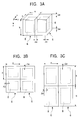
- FIG. 1 shows a thin-film capacitor device 1 of a first embodiment according to the present invention.
- the thin-film capacitor device 1 has a substrate 2 having a rectangular shape in plan view, a first electrode layer (lower electrode layer) 3, a second dielectric thin-film 5, a first dielectric thin-film 4, and a second electrode layer (upper electrode layer) 7, which are deposited on the substrate 2 in that order.
- a thin-film capacitor K is composed of the first dielectric thin-film 4 and the second dielectric thin-film 5.
- the material of the substrate 2 is not limited as long as it has a sufficient thickness to provide an appropriate stiffness to the entire capacitor device.
- the material is also resistant to a deposition temperature while the above layers are deposited on the substrate 2.
- An exemplary material satisfying the above conditions is a silicon-covered member such as a silicon wafer or a substrate made of SiO 2 or Al 2 O 3 .
- the first electrode layer 3 and the second electrode layer 7 may have a single layer structure made of a single metal such as Cu, Ag, Au, and Pt, or may have a multilayer structure.
- the multilayer structure may have at least two selected from the group consisting of a silicon oxide layer, a chromium layer, a nickel layer, a chromium oxide layer, a nickel oxide layer, and a platinum layer.
- the first dielectric thin-film 4 has a higher dielectric strength and a higher Q factor than those of the second dielectric thin-film 5, and the dielectric strength and the Q factor preferably changes slightly according to changes in temperature.
- the first dielectric thin-film 4 preferably has a temperature coefficient of capacitance with an absolute value of 50 ppm/°C or less, a relative dielectric constant of 10 or less, a field strength of 5 MV/cm or more and more preferably 8 MV/cm or more, an unloaded Q factor of 200 or more and more preferably 500 or more (at a frequency of 1 GHz or more), and a dielectric relaxation time of 1 second or more.
- the first dielectric thin-film 4 has a thickness of 1 ⁇ m (1 ⁇ 10 -6 m) or less, and more preferably 250 to 5,000 ⁇ (0.025 to 0.5 ⁇ m). Satisfying the above conditions provides an appropriate dielectric strength to the thin-film capacitor device 1; thereby achieving high productivity and reduction in the thickness.
- An exemplary material satisfying the above conditions includes amorphous SiO x N y and SiO x .
- An amorphous SiO x N y layer may be formed by a sputtering process or a PECVD process.
- the second dielectric thin-film 5 may have a lower dielectric strength and a lower Q factor than those of the first dielectric thin-film 4, and it is preferable that the changes in the dielectric strength and in the Q factor of the second dielectric thin-film 5 according to changes in temperature are larger than the changes in those of the first dielectric thin-film 4.
- the second dielectric thin-film 5 preferably has a negative temperature coefficient of capacitance with an absolute value of 500 ppm/°C or more, a relative dielectric constant of 150 or less, a unloaded Q factor of 50 or more and more preferably 100 or more (at a frequency of 1 GHz or more), and a dielectric relaxation time of 1 second or more.
- the second dielectric thin-film 5 has a thickness of 1 ⁇ m or less, preferably 0.025 ⁇ m (250 ⁇ ) to 0.5 ⁇ m (5,000 ⁇ ), and more preferably 0.025 ⁇ m (250 ⁇ ) to 0.3 ⁇ m (3,000 ⁇ ).
- the above conditions are based on the following reasons: preventing a plurality of grain boundaries from forming in the thickness direction of the layer when principal crystal grains included in the second dielectric thin-film 5 have a length of, for example, 0.5 ⁇ m to 1 ⁇ m in the planar direction; and reducing a deposition time as much as possible even if a thick layer is formed.
- the second dielectric thin-film 5 has a structure in which each of the principal crystal grains is surrounded by grain boundary layers, which will be described below.
- the above conditions are further based on the reason for preventing a large number of grain boundaries, for example, 10 or more, from forming in the thickness direction when the principal crystal grains have a diameter of, for example, 0.1 ⁇ m to 0.5 ⁇ m.
- the number of grain boundaries is preferably small and more preferably two or less, and it is ideal if no grain boundary exists in the thickness direction, that is, only a single grain exists in the thickness direction.
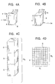
- the structure of the second dielectric thin-film 5 is described according to a crystal aggregation model shown in FIG. 3A.
- a principal grain unit 6 is assumed to be a rectangular parallelepiped having a height b in the Z direction (in the thickness direction) and a square (having both sides of length a in the planar direction) with a side of length of a in the X direction and with another side of length of a in the Y direction.
- the length of a side in the X direction is a -2 ⁇ a
- the length of the other side in the Y direction is a -2 ⁇ a
- the length of the height in the Z direction is b -2 ⁇ a .
- a large number of the principal grain units 6 having the above dimensions are arranged in the planar direction and in the thickness direction in the second dielectric thin-film 5.
- ⁇ (x) is used to indicate that ⁇ represents the relative dielectric constant and ⁇ is a function of x .
- ⁇ g represents the relative dielectric constant of the grain and ⁇ gb represents the relative dielectric constant of the grain boundary.
- the temperature coefficient of capacitance is defined as follows: ⁇ ( ⁇ / ⁇ T)/ ⁇ , wherein T represents the absolute temperature.
- T represents the absolute temperature.
- This formula indicates changes in the relative dielectric constant ⁇ (or the temperature coefficient of capacitance) according to changes in temperature.
- ⁇ / ⁇ is an important parameter in forming thin-films.
- the principal grain 8 has a width of a -2 ⁇ a in the X direction (in the planar direction), another width of a -2 ⁇ a in the Y direction (in the planar direction), and a height b in the Z direction (in the thickness direction).
- C g (1) represents the capacitance of a capacitor having a microstructure in which electrode layers are placed on and under the principal grain 8
- formula (6) is obtained as follows:
- C g (1) ⁇ g b - 2 ⁇ a (a - 2 ⁇ a) 2
- ⁇ represents the dielectric constant
- ⁇ represents the relative dielectric constant
- ⁇ 0 represents the dielectric constant of vacuum
- the principal grain unit 6 has a structure in which the grain boundary layers having a thickness of ⁇ a are placed on the four lateral faces of the principal grain 8.
- FIG. 4C shows a structure in which the N 3 principal grain units 6 are longitudinally arranged.
- C (1B) represents the capacitance of this structure
- FIG. 4D shows a structure in which the N 1 ⁇ N 2 units are arranged in plan view.
- the capacitance C (1B) of the structure in which N 3 units are longitudinally arranged is determined according to formula (9).
- the capacitance of the second dielectric thin-film having the N 1 ⁇ N 2 units is expressed by formula (10), that is, the formula shows the total capacitance of the second dielectric thin-film.
- formula (12) is derived into formula (13) as follows:
- the relative dielectric constant can be obtained using formula (3) and the normalized temperature coefficient of capacitance can be obtained using formula (4).
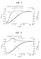
- FIG. 5 shows the calculation results based on the assumption that the relative dielectric constant ⁇ g and the ratio ⁇ g / ⁇ g of the principal grain unit are ten times greater than those of the grain boundary.
- FIG. 6 shows the calculation results based on the assumption that the relative dielectric constant ⁇ g and the temperature coefficient of capacitance ⁇ g of the principal grain unit are ten times greater than those of the grain boundary.
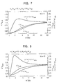
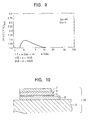
- FIGS. 7 and 8 show that the maximum value of the ⁇ / ⁇ ratio increases as the value of b/a increases.
- FIGS. 6 to 8 show that ( ⁇ / ⁇ )/( ⁇ / ⁇ ) bulk in the vertical axis has a value exceeding 1 in some regions.
- a thin-film capacitor device having such a second dielectric thin-film it is possible to estimate the value of ( ⁇ / ⁇ )/( ⁇ / ⁇ ) bulk , which exceeds 1, and to reduce the thickness of the dielectric thin-film compared with a conventional one by controlling a /2 ⁇ a in an appropriate range, for example, 2 to 12.
- FIG. 9 shows that ( ⁇ / ⁇ )/( ⁇ / ⁇ ) bulk exceeds 1, that is, it is in the range of 1.7 ⁇ a /2 ⁇ a ⁇ 13.
- the grain boundary layer has a thickness ⁇ a of 5 ⁇ and a boundary layer between the electrode layer and the dielectric thin-film has a thickness of 50 ⁇ and the dielectric thin-film estimated on the basis of an ideal single crystal has a thickness in the ranges of 250 ⁇ to 500 ⁇ , 500 ⁇ to 1,000 ⁇ , 1,000 ⁇ to 2,000 ⁇ , 2,000 ⁇ to 5,000 ⁇ , and 5,000 ⁇ to 10,000 ⁇
- the preferable grain size, the desired thickness, and a decrease in the thickness of the dielectric thin-film shown in Table 1 are obtained; wherein the thickness of the dielectric thin-film formed by adjusting the grain size in the above range is obtained by calculation.
- Thickness of Single Crystal Grain Size Maximum Decrease in Thickness 250 ⁇ to 500 ⁇ 13 ⁇ ⁇ a ⁇ 50 ⁇ 85 ⁇ ⁇ b ⁇ thickness 38% 500 ⁇ to 1,000 ⁇ 12 ⁇ ⁇ a ⁇ 80 ⁇ 60 ⁇ ⁇ b ⁇ thickness 57% 1,000 ⁇ to 2,000 ⁇ 12 ⁇ ⁇ a ⁇ 110 ⁇ 60 ⁇ ⁇ b ⁇ thickness 60% 2,000 ⁇ to 5,000 ⁇ 12 ⁇ ⁇ a ⁇ 130 ⁇ 60 ⁇ ⁇ b ⁇ thickness 62% 5,000 ⁇ to 10,000 ⁇ 12 ⁇ ⁇ a ⁇ 240 ⁇ 50 ⁇ ⁇ b ⁇ thickness 63%
- controlling the grain diameter a and the grain height b provides a 38% to 63% reduction in the thickness compared with that of dielectric thin-films made of a single crystal, that is, ones produced by conventional methods.
- the present invention provides a dielectric thin-film having a thickness less than that of the conventional one and a desired temperature coefficient of capacitance by controlling the above parameters.
- FIG. 9 shows that the parameters are preferably controlled in the range of 1.7 ⁇ a /2 ⁇ a ⁇ 13 and 5 ⁇ b/a to achieve a 10% or more reduction in thickness and are preferably controlled in the range of 1.8 ⁇ a /2 ⁇ a ⁇ 6 and 5 ⁇ b/a to achieve a 25% or more reduction in thickness.
- An exemplary material of the second dielectric thin-film 5 satisfying the above conditions includes crystalline Sr x Ba 1-x TiO 3 , crystalline CaTiO 3 , crystalline PbTiO 3 , and TiO 2 .
- Crystalline Sr x Ba 1-x TiO 3 , crystalline CaTiO 3 , and crystalline PbTiO 3 each have a phase transition temperature less than room temperature, a negative temperature coefficient of dielectric constant, and a relative dielectric constant of 100 or more at room temperature.
- the second dielectric thin-film 5 made of the above material is provided in combination with the first dielectric thin-film 4 to adjust the temperature coefficient of capacitance of the capacitor, there is a problem in that a leakage current arises due to the low dielectric strength of the second dielectric thin-film 5.
- a layer made of the above material may be formed by a deposition method such as sputtering.
- the thin-film capacitor 1 having the above configuration has an excellent dielectric strength due to the high dielectric strength of the first dielectric thin-film 4.
- the thin-film capacitor device 1 has a multilayer structure having the first dielectric thin-film 4 and the second dielectric thin-film 5, that is, the structure is different from that of conventional sheet dielectric ceramics, thereby easily achieving a reduction in thickness, miniaturization, and a capacitor having a thickness of 5 ⁇ m or less.
- the Q factor, the dielectric strength, and the temperature coefficient of capacitance of the capacitor can be adjusted by controlling the thicknesses of the first dielectric thin-film 4 and the second dielectric thin-film 5, and the composition thereof, thereby obtaining the thin-film capacitor device 1 having an excellent temperature stability in an operating environment in which changes in temperature are large.
- the thin-film capacitor 1 shown in FIG. 1 is suitable for electronic devices such as portable electronic devices and microwave communication devices, which need temperature compensation.
- the capacitor may be used in combination with a varactor diode that is an element for controlling the oscillation frequency according to voltage.
- the second dielectric thin-film 5 and the first dielectric thin-film 4 are deposited on the first electrode layer 3 in that order, and, as shown in FIG. 10, the first dielectric thin-film 4 may be deposited on the second dielectric thin-film 5 to form a thin-film capacitor device 10.
- the thin-film capacitor device 10 has the same effects as the thin-film capacitor device 1 of the first embodiment.
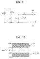
- FIG. 11 shows an exemplary resonant circuit in which a capacitor device C 1 , which is the thin-film capacitor device 1 or 10 according to the present invention is used.
- a capacitor device C 0 and a varactor diode D c are connected in parallel to the coil L.
- the thin-film capacitor device C 1 is connected in parallel to the varactor diode D c , the upper layer 7 and the upper layer 3 of the.
- thin-film capacitor device C 1 are connected to input-output terminals 11 and 12, respectively, and a resistance R is placed between the input-output terminals 12 and the thin-film capacitor device C 1 .
- the capacitance of the varactor diode D c changes according to voltage and the varactor diode Dc has a positive temperature coefficient of capacitance. Since the negative temperature coefficient of capacitance of the thin-film capacitor device C 1 compensates for that of the varactor diode D c , the resonant circuit is stable under changes in temperature.
- FIG. 12 shows the distribution of the temperature coefficients of capacitance thereof.
- the temperature coefficient of capacitance of varactor diode Dc is in the range of 200 ppm/°C to 500 ppm/°C and the temperature coefficient of capacitance of the thin-film capacitor device C 1 is in the range of -200 ppm/°C to -500 ppm/°C
- adjusting both temperature coefficients of capacitance to appropriate values improves the temperature stability of the circuit.
- the temperature coefficient of capacitance has not been controlled in such a wide range.
- the thin-film capacitor device C 1 produced by the method according to the present invention surely has a temperature coefficient of capacitance of -220 ppm/°C to -470 ppm/°C.
- Such a thin-film capacitor device can be widely used for temperature compensation and can be used for, for example, performing temperature compensation of a circuit using a varactor diode.
- FIG. 13 shows an exemplary structure of a two-frequency excitation-type sputtering system suitable for forming the second dielectric thin-film 2.
- the sputtering system A has a first high frequency power source 20, a first electrode 24, and a matching circuit 22A placed therebetween.
- the matching circuit 22A adjusts impedance between the first high frequency power source 20 and the first electrode 24.
- High frequency electricity from the first high frequency power source 20 is supplied to the first electrode 24 through the matching circuit 22A and a feeder board 23.
- the matching circuit 22A is housed in a matching box 22 which is a housing made of a conductor.
- the first electrode 24 and the feeder board 23 are covered with a chassis 21 made of a conductor.
- a recessed portion 24a is provided below the first electrode 24, and a target 25 is detachably mounted to the recessed portion 24a in a fitted manner.
- a deposition chamber 28, which is surrounded by chamber walls 27, is provided below the target 25, and the chassis 21 is disengaged from the chamber walls 27 by an insulator 29.
- the deposition chamber 28 is connected to a vacuum pumping system with pipes, and the deposition chamber 28 is controlled in a reduced-pressure atmosphere, for example, 10 -7 Pa.
- the apparatus and pipes of the vacuum pumping system are not shown in FIG. 13.
- the deposition chamber 28 has a second electrode 30, a box-shaped shield support 31 supporting the second electrode 30, a substrate 33 which is made of glass or the like and placed on the second electrode 30, and a supporting bottom plate 32 attached under the chamber walls 27 to partition the deposition chamber 28.
- a shaft 35 is connected to the second electrode 30 through the bottom of the shield support 31.
- the shaft 35 is connected to a second matching circuit 36A housed in a second matching box 36 through a partition 36 provided at the bottom of the shield support 31.
- the second matching circuit 35A is connected to a second high frequency power source 37.
- the first high frequency power source 20 supplies electricity with a power of 1-3 kW and with a frequency of 13.56 MHz to the first electrode 24 and the second high frequency power source 37 supplies electricity with a frequency of 40 MHz to the second electrode 30; thereby creating plasma between the first electrode 24 and the second electrode 30.
- the plasma generates the component particles from the target 25 to deposit the particles on the substrate 33 and a required thin-film is formed on the substrate 33.
- the pressure is preferably maintained at about 10 -7 Pa.
- High purity Ar gas which is supplied to the deposition chamber 28, preferably has an impurity content of 1 ppb or less.
- the deposition surface of the substrate 33 is cleaned with plasma created by supplying electricity with 13.56 MHz from the first high frequency power source 20.
- the electricity from the second high frequency power source 37 is used as bias electricity for the substrate 33; thereby performing sputtering by two-frequency excitation ion irradiation.
- the first high frequency power source 20 supplies electricity with a frequency of 13.56 MHz and the second high frequency power source 37 supplies electricity with a frequency of 40 MHz to perform deposition.
- the grain size of the dielectric thin-film is adjusted by controlling the power of the electricity which is supplied from the second high frequency power source 37 and is applied to the substrate as bias electricity.
- a dielectric thin-film including longitudinal principal crystal grains and one or two grain boundaries in the thickness direction is obtained when electricity with a power of 1.5 kW is supplied from the first high frequency power source 20 and bias electricity with a power of 0 W is supplied from the second high frequency power source 37.
- Another dielectric thin-film including principal crystal grains having a small diameter in the planar direction and including several dozen grain boundaries in the thickness direction is obtained when electricity with a power of 1.5 kW is supplied from the first high frequency power source 20 and bias electricity with a power of 200 W is supplied from the second high frequency power source 37.
- the grain diameter in the planar direction and the grain height in the thickness direction are adjusted by applying the bias electricity with a power in the above range, that is, 0-200 W.
- Exemplary preferable conditions for manufacturing a TiO 2 dielectric thin-film are as follows: an O 2 partial pressure of 30-90% in an Ar atmosphere gas, electricity with a frequency of 1-3 kW from a first high frequency power source, electricity with a power of 0-400 W from a second high frequency power source, and a pressure of 0.5-1.0 Pa in a deposition chamber. Adding impurities such as gaseous N 2 and the like to the atmosphere gas is also effective in adjusting the grain size.
- the grain size of the second dielectric thin-film can be adjusted by the above method and the properties of the second dielectric thin-film satisfies the condition ⁇ ( ⁇ / ⁇ )/( ⁇ g / ⁇ g ) ⁇ > 1; thereby achieving reduction in the thickness of the dielectric thin-film.
- a Cu lower electrode having a thickness of 1.3 ⁇ m was deposited on an alumina or glass substrate at room temperature.
- CaTiO 3 thin-films (second dielectric thin-film) each having a thickness of 2400 ⁇ , 3500 ⁇ and 4700 ⁇ were deposited on the lower electrode, adjusting the grain size by a sputtering process under the conditions described below.
- a-SiN x thin-films (first dielectric thin-film) each having a thickness of 900 ⁇ , 700 ⁇ and 500 ⁇ were deposited, adjusting the grain size by a sputtering process under the conditions described below.
- a Cu upper electrode having a thickness of 1.3 ⁇ m was finally deposited by a sputtering process at room temperature to complete a multilayered thin-film capacitor device. These capacitors had a sheet capacitance of 480 pF/mm 2 .
- the two-frequency excitation-type sputtering system described above was used and the power of bias electricity was changed in the range of 0-300 W.
- each of the thin-film capacitor devices prepared by the method according to present invention has a smaller thickness than that of each of the corresponding conventional thin-film capacitor devices when each thin-film capacitor device of the present invention has the same temperature coefficients as that of each corresponding conventional thin-film capacitor device. That is, for the second dielectric thin-films, the thickness can be reduced from 4100 ⁇ to 2400 ⁇ , from 6100 ⁇ to 3500 ⁇ , and from 8700 ⁇ to 2700 ⁇ ; thereby achieving a significant reduction in thickness.
- the thickness can be reduced and the temperature coefficient of capacitance can be controlled in the range of -220 to -470 ppm/°C; hence, such devices suitably performs temperature compensation of elements such as varactor diode having a positive temperature coefficient of capacitance.
- FIGS. 14 and 15 depict photographs showing sectional structures, each having a TiO 2 layer formed using a two-frequency excitation-type sputtering system shown in FIG. 13.
- the layered structure shown in FIG. 14 has a glass substrate and a Cr electrode layer, the TiO 2 layer, and another Cr electrode layer which are deposited on the glass substrate in that order.
- the TiO 2 layer was formed under the following conditions: an O 2 partial pressure of 80%, electricity with a power of 1.5 kW from the first high frequency power source, electricity with a power of 0 W from the second high frequency power source, and a total pressure of 4 Pa in the deposition chamber.
- the other layered structure shown in FIG. 15 has a glass substrate and a Cr electrode layer, the TiO 2 layer, and another Cr electrode layer which are deposited on the glass substrate in that order.
- the TiO 2 layer was formed under the following conditions: an O 2 partial pressure of 80%, electricity with a power of 1.5 kW from the first high frequency power source, electricity with a power of 200 W from the second high frequency power source, and a total pressure of 4 Pa in the deposition chamber.
- the former layered structure shown in FIG. 14 has one or two grain boundaries in the thickness direction
- the latter layered structure shown in FIG. 15 has several dozen grain boundaries in the thickness direction.
- the present invention provides a thin-film capacitor device having a pair of electrode layers sandwiching a first dielectric thin-film and a second dielectric thin-film.
- the size of a principal crystal grain of the second dielectric thin-film is adjusted to a desired value; thereby achieving a reduction in the thickness of the second dielectric thin-film and subsequently achieving a reduction in the thickness of the entire thin-film capacitor device.
- the first and second dielectric thin-films are sandwiched between the electrode layers; thereby achieving the adjustment of the Q factor and the dielectric strength and also performing temperature compensation.
- the temperature coefficient can be adjusted in a wide range; thereby allowing the capacitor to perform temperature compensation.
- the ratio ⁇ ( ⁇ / ⁇ )/( ⁇ g / ⁇ g ) ⁇ may exceed 1.
- the ratio a/b of the principal crystal grain is constant, the ratio a /2 ⁇ a may be determined such that the ratio ⁇ ( ⁇ / ⁇ )/( ⁇ g / ⁇ g ) ⁇ exceeds 1, in the relationship between the ratio a /2 ⁇ a and the ratio ⁇ / ⁇ .
- the second dielectric thin-film is made of any one selected from the group consisting of Sr x Ba 1-x TiO 3 , CaTiO 3 , and PbTiO 3 , adjustment of the temperature coefficient and a reduction in the thickness can be easily achieved by adjusting the grain size.
- temperature compensation is possible in a wide range. Efficient temperature compensation is possible in combination with a varactor diode having a positive temperature coefficient.
Landscapes
- Fixed Capacitors And Capacitor Manufacturing Machines (AREA)
- Semiconductor Integrated Circuits (AREA)
Applications Claiming Priority (2)
| Application Number | Priority Date | Filing Date | Title |
|---|---|---|---|
| JP2001089528 | 2001-03-27 | ||
| JP2001089528A JP2002289462A (ja) | 2001-03-27 | 2001-03-27 | 薄膜キャパシタの製造方法とその薄膜キャパシタを備えた温度補償用薄膜コンデンサ及び電子機器と電子回路 |
Publications (2)
| Publication Number | Publication Date |
|---|---|
| EP1246232A2 true EP1246232A2 (de) | 2002-10-02 |
| EP1246232A3 EP1246232A3 (de) | 2006-06-07 |
Family
ID=18944446
Family Applications (1)
| Application Number | Title | Priority Date | Filing Date |
|---|---|---|---|
| EP02252172A Withdrawn EP1246232A3 (de) | 2001-03-27 | 2002-03-26 | Herstellungsmethode eines Dünnschichtkondensators für die Temperaturkompensation von Übergangskapazitäten in Halbleiteranordnungen |
Country Status (4)
| Country | Link |
|---|---|
| US (2) | US6605515B2 (de) |
| EP (1) | EP1246232A3 (de) |
| JP (1) | JP2002289462A (de) |
| CN (1) | CN1225754C (de) |
Families Citing this family (30)
| Publication number | Priority date | Publication date | Assignee | Title |
|---|---|---|---|---|
| US6606515B1 (en) * | 1996-09-13 | 2003-08-12 | Scimed Life Systems, Inc. | Guide wire insertion and re-insertion tools and methods of use |
| US8181338B2 (en) | 2000-11-02 | 2012-05-22 | Danfoss A/S | Method of making a multilayer composite |
| US7548015B2 (en) * | 2000-11-02 | 2009-06-16 | Danfoss A/S | Multilayer composite and a method of making such |
| US7518284B2 (en) | 2000-11-02 | 2009-04-14 | Danfoss A/S | Dielectric composite and a method of manufacturing a dielectric composite |
| ES2299614T3 (es) | 2001-12-21 | 2008-06-01 | Danfoss A/S | Estructura de dispositivo dielectrico de accionamiento o deteccion y metodo para fabricar el mismo. |
| JP4166013B2 (ja) * | 2001-12-26 | 2008-10-15 | 富士通株式会社 | 薄膜キャパシタ製造方法 |
| CN100530931C (zh) * | 2002-09-20 | 2009-08-19 | 丹福斯有限公司 | 弹性体致动器及制造致动器的方法 |
| US20040061990A1 (en) * | 2002-09-26 | 2004-04-01 | Dougherty T. Kirk | Temperature-compensated ferroelectric capacitor device, and its fabrication |
| DE60328913D1 (de) * | 2002-12-12 | 2009-10-01 | Danfoss As | Berührungssensorelement und sensorgruppe |
| DK1596794T3 (da) | 2003-02-24 | 2008-10-27 | Danfoss As | Elektroaktiv elastisk bandage |
| US20040190225A1 (en) * | 2003-03-28 | 2004-09-30 | Nippon Paint Co., Ltd. | Silicon-containing compound, sintered body of silicon-containing compound, and producing method thereof, and completely solid type capacitor element using same |
| JP4523299B2 (ja) * | 2003-10-31 | 2010-08-11 | 学校法人早稲田大学 | 薄膜コンデンサの製造方法 |
| JP2005252069A (ja) * | 2004-03-05 | 2005-09-15 | Tdk Corp | 電子デバイス及びその製造方法 |
| JP4370217B2 (ja) * | 2004-07-29 | 2009-11-25 | Tdk株式会社 | 積層セラミックコンデンサ |
| US9572258B2 (en) * | 2004-12-30 | 2017-02-14 | Intel Corporation | Method of forming a substrate core with embedded capacitor and structures formed thereby |
| US7288459B2 (en) * | 2005-03-31 | 2007-10-30 | Intel Corporation | Organic substrates with integral thin-film capacitors, methods of making same, and systems containing same |
| US7372126B2 (en) * | 2005-03-31 | 2008-05-13 | Intel Corporation | Organic substrates with embedded thin-film capacitors, methods of making same, and systems containing same |
| US7880371B2 (en) | 2006-11-03 | 2011-02-01 | Danfoss A/S | Dielectric composite and a method of manufacturing a dielectric composite |
| US7732999B2 (en) * | 2006-11-03 | 2010-06-08 | Danfoss A/S | Direct acting capacitive transducer |
| US7902564B2 (en) * | 2006-12-22 | 2011-03-08 | Koninklijke Philips Electronics N.V. | Multi-grain luminescent ceramics for light emitting devices |
| US8184426B2 (en) * | 2006-12-25 | 2012-05-22 | National Institute For Materials Science | Dielectric element and method for producing the dielectric element |
| US7804678B2 (en) | 2007-04-25 | 2010-09-28 | Industrial Technology Research Institute | Capacitor devices |
| US8047073B2 (en) * | 2007-05-14 | 2011-11-01 | Samsung Sdi Co., Ltd. | Capacitive liquid level detector for direct methanol fuel cell systems |
| US8101495B2 (en) | 2008-03-13 | 2012-01-24 | Infineon Technologies Ag | MIM capacitors in semiconductor components |
| JP5332989B2 (ja) * | 2009-07-10 | 2013-11-06 | ソニー株式会社 | 液体タンクおよび燃料電池 |
| US8891222B2 (en) | 2012-02-14 | 2014-11-18 | Danfoss A/S | Capacitive transducer and a method for manufacturing a transducer |
| US8692442B2 (en) | 2012-02-14 | 2014-04-08 | Danfoss Polypower A/S | Polymer transducer and a connector for a transducer |
| US10748986B2 (en) | 2017-11-21 | 2020-08-18 | Taiwan Semiconductor Manufacturing Co., Ltd. | Structure and formation method of semiconductor device with capacitors |
| EP3796383A4 (de) * | 2019-07-26 | 2021-03-31 | Shenzhen Goodix Technology Co., Ltd. | Kapazitive vorrichtung und herstellungsverfahren dafür |
| US11869725B2 (en) * | 2021-11-30 | 2024-01-09 | Texas Instruments Incorporated | Multi-stacked capacitor |
Family Cites Families (10)
| Publication number | Priority date | Publication date | Assignee | Title |
|---|---|---|---|---|
| JPS60124303A (ja) | 1983-12-08 | 1985-07-03 | 沖電気工業株式会社 | マイクロ波用誘電体セラミックス |
| US6002578A (en) * | 1986-08-22 | 1999-12-14 | Canon Kabushiki Kaisha | Ceramic substrate, circuit substrate and electronic circuit substrate by use thereof and method for preparing ceramic substrate |
| JPS63110618A (ja) | 1986-10-28 | 1988-05-16 | 沖電気工業株式会社 | 積層型マイクロ波用誘電体磁器組成物 |
| JPH0648666B2 (ja) * | 1987-09-29 | 1994-06-22 | 三菱マテリアル株式会社 | 積層セラミックコンデンサ及びその製法 |
| JPH03252160A (ja) * | 1990-02-28 | 1991-11-11 | Nec Corp | コンデンサ、コンデンサネットワーク及び抵抗―コンデンサネットワーク |
| EP0749134B1 (de) | 1995-06-16 | 2002-10-02 | AT&T IPM Corp. | TiO2 dotiertes, Ta2O5 enthaltendes dielektrisches Material und dieses enthaltende Bauteile |
| JPH09293629A (ja) * | 1996-04-26 | 1997-11-11 | Mitsubishi Materials Corp | 薄膜コンデンサ |
| US5978207A (en) * | 1996-10-30 | 1999-11-02 | The Research Foundation Of The State University Of New York | Thin film capacitor |
| US6251816B1 (en) * | 1998-12-31 | 2001-06-26 | Mra Laboratories, Inc. | Capacitor and dielectric ceramic powder based upon a barium borate and zinc silicate dual-component sintering flux |
| US6482527B1 (en) * | 1999-10-27 | 2002-11-19 | The Penn State Research Foundation | Pyrochlore thin films and process for making |
-
2001
- 2001-03-27 JP JP2001089528A patent/JP2002289462A/ja not_active Withdrawn
-
2002
- 2002-03-18 US US10/100,935 patent/US6605515B2/en not_active Expired - Fee Related
- 2002-03-26 EP EP02252172A patent/EP1246232A3/de not_active Withdrawn
- 2002-03-27 CN CNB021085153A patent/CN1225754C/zh not_active Expired - Fee Related
-
2003
- 2003-05-30 US US10/452,246 patent/US6747334B2/en not_active Expired - Fee Related
Also Published As
| Publication number | Publication date |
|---|---|
| EP1246232A3 (de) | 2006-06-07 |
| CN1225754C (zh) | 2005-11-02 |
| CN1378223A (zh) | 2002-11-06 |
| US6747334B2 (en) | 2004-06-08 |
| US20030008470A1 (en) | 2003-01-09 |
| US20030213960A1 (en) | 2003-11-20 |
| US6605515B2 (en) | 2003-08-12 |
| JP2002289462A (ja) | 2002-10-04 |
Similar Documents
| Publication | Publication Date | Title |
|---|---|---|
| US6605515B2 (en) | Method for manufacturing thin-film capacitor for performing temperature compensation of junction capacitance of semiconductor device | |
| Herbert | Ceramic dielectrics and capacitors | |
| US9136819B2 (en) | Bulk acoustic wave resonator having piezoelectric layer with multiple dopants | |
| KR100450101B1 (ko) | 온도 보상용 박막 콘덴서 | |
| US8194387B2 (en) | Electrostrictive resonance suppression for tunable capacitors | |
| US8953299B2 (en) | Capacitors adapted for acoustic resonance cancellation | |
| US9269496B2 (en) | Capacitors adapted for acoustic resonance cancellation | |
| US6617062B2 (en) | Strain-relieved tunable dielectric thin films | |
| JP7387102B2 (ja) | 膜構造体及びその製造方法 | |
| US20100182730A1 (en) | Ferroelectric varactor with improved tuning range | |
| US20150274600A1 (en) | Dielectric composition and electronic component | |
| CN102667982A (zh) | 变容二极管和用于制造变容二极管的方法 | |
| US20180061931A1 (en) | Microstructural architecture to enable strain relieved non-linear complex oxide thin films | |
| CN108695063B (zh) | 氧氮化物薄膜及电容元件 | |
| JP4493235B2 (ja) | 薄膜素子 | |
| TWI760346B (zh) | 成膜裝置 | |
| WO2006034119A1 (en) | BST INTEGRATION USING THIN BUFFER LAYER GROWN DIRECTLY ONTO SiO2/Si SUBSTRATE | |
| Bogner et al. | Enhanced Piezoelectric $\mathrm {AL} _ {1-\mathrm {X}}\mathrm {SC} _ {\mathrm {X}}\mathrm {N} $ RF-MEMS Resonators for Sub-6 GHz RF-Filter Applications: Design, Fabrication and Characterization | |
| Yamada et al. | Piezoelectric properties of La-doped PbTiO3 films for RF resonators | |
| JP2839629B2 (ja) | 誘電体薄膜及び薄膜コンデンサ | |
| Bellotti | Strain and thickness effects on the microwave properties of barium strontium titanate thin films | |
| TW200410271A (en) | Capacitor composite circuit element and IC card multilayer capacitor |
Legal Events
| Date | Code | Title | Description |
|---|---|---|---|
| PUAI | Public reference made under article 153(3) epc to a published international application that has entered the european phase |
Free format text: ORIGINAL CODE: 0009012 |
|
| AK | Designated contracting states |
Kind code of ref document: A2 Designated state(s): AT BE CH CY DE DK ES FI FR GB GR IE IT LI LU MC NL PT SE TR |
|
| AX | Request for extension of the european patent |
Free format text: AL;LT;LV;MK;RO;SI |
|
| PUAL | Search report despatched |
Free format text: ORIGINAL CODE: 0009013 |
|
| AK | Designated contracting states |
Kind code of ref document: A3 Designated state(s): AT BE CH CY DE DK ES FI FR GB GR IE IT LI LU MC NL PT SE TR |
|
| AX | Request for extension of the european patent |
Extension state: AL LT LV MK RO SI |
|
| 17P | Request for examination filed |
Effective date: 20060621 |
|
| 17Q | First examination report despatched |
Effective date: 20061002 |
|
| AKX | Designation fees paid |
Designated state(s): DE FI FR GB |
|
| STAA | Information on the status of an ep patent application or granted ep patent |
Free format text: STATUS: THE APPLICATION IS DEEMED TO BE WITHDRAWN |
|
| 18D | Application deemed to be withdrawn |
Effective date: 20070213 |