EP1237140A1 - Circuit de commande d'un dispositif d'affichage - Google Patents
Circuit de commande d'un dispositif d'affichage Download PDFInfo
- Publication number
- EP1237140A1 EP1237140A1 EP02003965A EP02003965A EP1237140A1 EP 1237140 A1 EP1237140 A1 EP 1237140A1 EP 02003965 A EP02003965 A EP 02003965A EP 02003965 A EP02003965 A EP 02003965A EP 1237140 A1 EP1237140 A1 EP 1237140A1
- Authority
- EP
- European Patent Office
- Prior art keywords
- display
- control
- vfd
- led
- control signals
- Prior art date
- Legal status (The legal status is an assumption and is not a legal conclusion. Google has not performed a legal analysis and makes no representation as to the accuracy of the status listed.)
- Granted
Links
- 230000006870 function Effects 0.000 claims description 2
- 239000000284 extract Substances 0.000 claims 1
- 239000013078 crystal Substances 0.000 description 4
- 238000011161 development Methods 0.000 description 3
- 230000018109 developmental process Effects 0.000 description 3
- 238000010586 diagram Methods 0.000 description 2
- 241000554155 Andes Species 0.000 description 1
- 238000000149 argon plasma sintering Methods 0.000 description 1
- 230000000694 effects Effects 0.000 description 1
- 239000004973 liquid crystal related substance Substances 0.000 description 1
- 238000000034 method Methods 0.000 description 1
- 230000004044 response Effects 0.000 description 1
- 238000010561 standard procedure Methods 0.000 description 1
Images


Classifications
-
- G—PHYSICS
- G09—EDUCATION; CRYPTOGRAPHY; DISPLAY; ADVERTISING; SEALS
- G09G—ARRANGEMENTS OR CIRCUITS FOR CONTROL OF INDICATING DEVICES USING STATIC MEANS TO PRESENT VARIABLE INFORMATION
- G09G3/00—Control arrangements or circuits, of interest only in connection with visual indicators other than cathode-ray tubes
- G09G3/04—Control arrangements or circuits, of interest only in connection with visual indicators other than cathode-ray tubes for presentation of a single character by selection from a plurality of characters, or by composing the character by combination of individual elements, e.g. segments using a combination of such display devices for composing words, rows or the like, in a frame with fixed character positions
- G09G3/16—Control arrangements or circuits, of interest only in connection with visual indicators other than cathode-ray tubes for presentation of a single character by selection from a plurality of characters, or by composing the character by combination of individual elements, e.g. segments using a combination of such display devices for composing words, rows or the like, in a frame with fixed character positions by control of light from an independent source
- G09G3/18—Control arrangements or circuits, of interest only in connection with visual indicators other than cathode-ray tubes for presentation of a single character by selection from a plurality of characters, or by composing the character by combination of individual elements, e.g. segments using a combination of such display devices for composing words, rows or the like, in a frame with fixed character positions by control of light from an independent source using liquid crystals
-
- G—PHYSICS
- G09—EDUCATION; CRYPTOGRAPHY; DISPLAY; ADVERTISING; SEALS
- G09G—ARRANGEMENTS OR CIRCUITS FOR CONTROL OF INDICATING DEVICES USING STATIC MEANS TO PRESENT VARIABLE INFORMATION
- G09G3/00—Control arrangements or circuits, of interest only in connection with visual indicators other than cathode-ray tubes
- G09G3/04—Control arrangements or circuits, of interest only in connection with visual indicators other than cathode-ray tubes for presentation of a single character by selection from a plurality of characters, or by composing the character by combination of individual elements, e.g. segments using a combination of such display devices for composing words, rows or the like, in a frame with fixed character positions
-
- G—PHYSICS
- G09—EDUCATION; CRYPTOGRAPHY; DISPLAY; ADVERTISING; SEALS
- G09G—ARRANGEMENTS OR CIRCUITS FOR CONTROL OF INDICATING DEVICES USING STATIC MEANS TO PRESENT VARIABLE INFORMATION
- G09G2310/00—Command of the display device
- G09G2310/06—Details of flat display driving waveforms
-
- G—PHYSICS
- G09—EDUCATION; CRYPTOGRAPHY; DISPLAY; ADVERTISING; SEALS
- G09G—ARRANGEMENTS OR CIRCUITS FOR CONTROL OF INDICATING DEVICES USING STATIC MEANS TO PRESENT VARIABLE INFORMATION
- G09G3/00—Control arrangements or circuits, of interest only in connection with visual indicators other than cathode-ray tubes
- G09G3/04—Control arrangements or circuits, of interest only in connection with visual indicators other than cathode-ray tubes for presentation of a single character by selection from a plurality of characters, or by composing the character by combination of individual elements, e.g. segments using a combination of such display devices for composing words, rows or the like, in a frame with fixed character positions
- G09G3/06—Control arrangements or circuits, of interest only in connection with visual indicators other than cathode-ray tubes for presentation of a single character by selection from a plurality of characters, or by composing the character by combination of individual elements, e.g. segments using a combination of such display devices for composing words, rows or the like, in a frame with fixed character positions using controlled light sources
- G09G3/12—Control arrangements or circuits, of interest only in connection with visual indicators other than cathode-ray tubes for presentation of a single character by selection from a plurality of characters, or by composing the character by combination of individual elements, e.g. segments using a combination of such display devices for composing words, rows or the like, in a frame with fixed character positions using controlled light sources using electroluminescent elements
- G09G3/14—Semiconductor devices, e.g. diodes
Definitions
- the invention relates to a circuit arrangement for controlling a VFD, LED or LCD display.
- Such advertisements are e.g. widely used in small electrical appliances. You serve et al to display the time or temperature. With electronic stove time switches on such displays there are also signs for the set one Operating mode of the stove or oven or for other functions such as Alarm or radio reception. A numerical display (e.g. for the time) appears here usually realized using a 7-segment display.
- Such displays are controlled according to the type of each Display (VFD, LED, LCD) each different.
- VFD vacuum fluorescence display
- the individual, corresponding segments of the different (7-segment) digits are connected in parallel with each other and form the anodes.
- grids Between the heated cathodes and the segments serving as anodes are attached grids, which each extend over the area of a digit.
- a segment of a certain number lights up when both the anode corresponding to this segment as well as the one corresponding to this number Grid is at positive voltage. Via multiplex control of the segments and the digits are therefore each individual segment of each individual Number can be controlled separately.
- each segment In the case of a light-emitting diode display (LED), the individual segments are the digits each formed by individual light emitting diodes. The individual, corresponding to each other Segments of the different digits are again parallel to each other interconnects and form the cathode, while the various digits form the anodes.
- each segment can be controlled by means of multiplex can be addressed separately.
- VFD has either positive voltage at the connections or no voltage is applied while on the connections of the LED display positive (for digits) or negative (for segments) or no voltage applied becomes.
- VFD with a relatively high voltage of 16 operated up to 30 V, but low current of 0.1 to 2 mA, while an LED display only a small voltage of about 2 V, but a larger current of 2 up to 20 mA required.
- liquid crystal display LCD
- An LCD is now constructed in such a way that up to 3 segments are parallel to each other are connected and thus form an electrode.
- the other electrode is through three back electrodes (COM) formed, each one of the three with each other parallel connected segments are assigned.
- COM back electrodes
- This way is also here Multiplex control possible again.
- here are up to the individual Connections of the display not only two voltage values (positive or negative and zero), but also intermediate voltage values (in the described case 1/3 and 2/3 of the voltage) so that a targeted reloading of individual elements without Influencing the other elements is possible.
- the ability to drive a VFD, LED and LCD display is thereby achieved that at least two control blocks are provided, one of the Control blocks generates the control signals necessary for an LCD display and the other the one necessary for a VFD or LED or for both displays Control signals generated.
- the control signals of the control blocks become common Driver module supplied, the corresponding from these control signals Control signals for the VFD / LED display and for the LCD display are generated and passes it on to the corresponding ad.
- control blocks are provided, one of which one each for the LCD, VFD and LED displays the necessary control signals supplies.
- one or more storage elements can be provided are assigned to the individual control blocks.
- the driver module has several driver elements on, each with a connection of the VFD, LED or LCD display is connected and this connection a corresponding control signal supplies.
- each driver element with each of the Control blocks is connected so that it is all used to control the connection necessary control signals are supplied to the connected display.
- control signals of the control blocks in the driver elements are preferably such interconnects that the connection of the connected display the appropriate one Control signal is supplied. This interconnection takes place in a further development of Invention depending on the type of display connected.
- control logic, the at least one memory element and the Control blocks executed digitally, while the driver block executed analog is.
- a circuit arrangement 1 for controlling a VFD, LED or LCD display 2 has a data receiver 3, which is used to control the Display necessary data from a microprocessor 4, which receives the data receiver 3 simultaneously supplied with a time 4.1.
- the data receiver 3 passes the received data on to a control logic 5.
- the control logic 5 checks the received data and decodes it by extracting from the received Data addresses, control words and commands extracted. The commands contain the actual display data.
- This display data is sent to a data memory 6 passed on and saved there. They remain saved as long as until the display is to be changed. Then new display data in the Data memory 6 saved.
- control logic 5 shares a first control block 7, which is the generation of control signals required for an LCD display, and a second Control block 8, which the generation of for a VFD or LED display necessary Control signals, with which control mode is set (e.g. VFD / LED 5-fold, 6-fold or 7-fold multiplex, LCD 3-fold multiplex, night reduction or load shedding; see below).
- the selected mode is in the ROM block 9 stored, which is in operative connection with the control logic 5.
- control block 7 or control block 8 active. Using the data memory 6 The active control block 7 or 8 generates the display data provided in the usual way and further explained below for the respective display 2 necessary control signals COM 1 to 3 and S 1 to 13 (LCD) or G 1 to 7 and S 1 to 9 (VFD / LED) (see also below).
- the control signals from the control block 8 still pass through the level shifter 10, in which, in the presence of a VFD mode, the levels of the control signals from usual 3.3 V to 30 V necessary for a VFD. In the event of In LED mode, this level increase is not necessary.
- the information about the set mode receives the level shifter 10 as well as the control blocks 7 and 8 from the control logic 5.
- the control signals of the control blocks 7 and 8 then arrive at the driver module 11.
- both control blocks 7 and 8 can be independent of set mode are active at all times. In this case, however, it is necessary that the driver elements 11.1 to 11.16 control signals depending on the mode set (LCD or VFD / LED) received by only one of the control blocks 7 and 8. The the driver elements 11.1 to 11.16 receive corresponding information directly from the control logic 5.
- the control logic 5 also controls a reset circuit 12 for the microprocessor 4, a buzzer circuit 13 for a buzzer 14 and a driver 15 for controlling relays 16 and 17.
- a voltage supply for the individual components of the circuit arrangement 1 is not drawn for the sake of clarity; the power supply takes place however in the usual way.
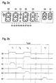
- Figure 2a shows the light segments of a VFD or an LED display. With a designated segments are interconnected in parallel and with the connector S1 connected, the elements labeled b to the terminal S2, etc.
- the connections G1 to G7 are each with a number (possibly connected with adjacent symbols) extending grid.
- the control for an LED display is basically the same as straight described, only that a negative instead of a positive at the connections S1 to S9 Voltage is present.
- the display elements of an LCD are shown in FIG. 3a. Up to three of each Display elements are interconnected in parallel and to connections S1 connected up to S13. The back electrodes of the three elements are each on the Connection COM 1, COM 2 or COM 3 connected.
- FIG 3b is the time course of the connections COM 1, COM 2 and COM 3 as well as signals present at connection S12, where it is a standard procedure for controlling an LCD.
- the Andes Connections S1 to S13 are compared to the signals at COM 1, COM 2 and COM 3 signals present in opposite polarity, so that e.g. on the upper display element S12 a voltage corresponding to COM 1 minus S12 is present, on the middle display element S12 corresponding to COM 2 minus S12 and on the lower display element S12 corresponding to COM 3 minus S12.
- the Voltage differences, which on the upper display element (accordingly COM 1 minus S12) are too small for the crystals to align could. There is therefore no display there. In the middle and lower Display element, however, large voltage differences of 2 U occur, which is why here an alignment of the crystals and thus an indication is given.
- FIG. 4 now shows a basic circuit diagram of the driver elements 11.1 to 11.16 each included circuitry for generating the control signals for the display 2.
- the control block 8 switches 18 and 19 driven by digital signals W4 and W0.
- a signal i.e. Voltage present
- the switch 18 is closed via a digital signal W4
- the switch 18 is opened and the Switch 19 closed by a digital signal W0.
- the (accordingly dimensioned) switches 18 and 19 for a VFD or LED element suitable signal are generated.
- Switches 19, 20, 21 and 22 are used to control an LCD element. By closing the corresponding switch using the associated, The digital signal W0, W1, W2 or W3 coming from the control block 7 can Voltage at output A can be adjusted to 0, 1/3 U, 2/3 U or U, where U is typically 3.3 V.
- the control logic 5, the memory element 6 and the control blocks 7 and 8 of the Circuit arrangement 1 are implemented digitally, while the driver module 11 is carried out analogously with the driver elements 11.1 to 11.16.
- the whole Circuit arrangement 1 is designed as an integrated circuit (IC). In these IC are also the reset circuit 12, the buzzer circuit 13 and the relay driver 15 integrated.
Landscapes
- Engineering & Computer Science (AREA)
- Physics & Mathematics (AREA)
- Computer Hardware Design (AREA)
- General Physics & Mathematics (AREA)
- Theoretical Computer Science (AREA)
- Chemical & Material Sciences (AREA)
- Crystallography & Structural Chemistry (AREA)
- Control Of Indicators Other Than Cathode Ray Tubes (AREA)
Applications Claiming Priority (2)
| Application Number | Priority Date | Filing Date | Title |
|---|---|---|---|
| DE10109157 | 2001-02-24 | ||
| DE10109157A DE10109157A1 (de) | 2001-02-24 | 2001-02-24 | Schaltungsanordnung zur Ansteuerung einer Anzeige |
Publications (2)
| Publication Number | Publication Date |
|---|---|
| EP1237140A1 true EP1237140A1 (fr) | 2002-09-04 |
| EP1237140B1 EP1237140B1 (fr) | 2005-11-02 |
Family
ID=7675500
Family Applications (1)
| Application Number | Title | Priority Date | Filing Date |
|---|---|---|---|
| EP02003965A Expired - Lifetime EP1237140B1 (fr) | 2001-02-24 | 2002-02-22 | Circuit de commande d'un dispositif d'affichage |
Country Status (4)
| Country | Link |
|---|---|
| US (1) | US6844864B2 (fr) |
| EP (1) | EP1237140B1 (fr) |
| DE (2) | DE10109157A1 (fr) |
| PL (1) | PL198894B1 (fr) |
Cited By (1)
| Publication number | Priority date | Publication date | Assignee | Title |
|---|---|---|---|---|
| US6025921A (en) * | 1995-01-23 | 2000-02-15 | Ohio Electronics Engravers, Inc. | Method and apparatus for engraving a mixed pattern |
Families Citing this family (3)
| Publication number | Priority date | Publication date | Assignee | Title |
|---|---|---|---|---|
| US7109957B2 (en) * | 1999-01-22 | 2006-09-19 | Au Optronics Corp. | Digital display driving circuit for light emitting diode display |
| DE10225996B4 (de) * | 2002-06-12 | 2006-01-12 | Diehl Ako Stiftung & Co. Kg | Ansteuerschaltung für eine Vakuumfluoreszenz-Anzeige |
| US7970439B2 (en) * | 2005-03-01 | 2011-06-28 | Kyocera Corporation | Systems and methods for visual alerting mechanisms on a mobile communication device |
Family Cites Families (17)
| Publication number | Priority date | Publication date | Assignee | Title |
|---|---|---|---|---|
| US3984973A (en) * | 1973-10-29 | 1976-10-12 | Hughes Aircraft Company | Digital watch with liquid crystal and light emitting diode displays |
| JPS5665537A (en) * | 1979-11-01 | 1981-06-03 | Nec Corp | Individual selection callout receiver with display |
| JPS56162588U (fr) | 1980-04-30 | 1981-12-03 | ||
| GB2075726B (en) | 1980-05-02 | 1983-11-23 | Suwa Seikosha Kk | Electronic timepiece |
| JPS58162988A (ja) * | 1982-03-23 | 1983-09-27 | 日本電気株式会社 | 表示装置 |
| US4542799A (en) * | 1982-04-28 | 1985-09-24 | Shimadzu Corporation | Display device for use in an electronic balance |
| JPS5991487A (ja) * | 1982-11-17 | 1984-05-26 | 富士通株式会社 | デイスプレイ装置 |
| JPS60227296A (ja) | 1984-04-25 | 1985-11-12 | シャープ株式会社 | 表示制御方式 |
| JPS61213896A (ja) * | 1985-03-19 | 1986-09-22 | 株式会社 アスキ− | デイスプレイコントロ−ラ |
| JPS6347791A (ja) * | 1986-08-15 | 1988-02-29 | 株式会社東芝 | 情報表示説明装置 |
| JPH01248186A (ja) * | 1988-03-30 | 1989-10-03 | Toshiba Corp | 表示属性変換装置 |
| US5021775A (en) * | 1989-02-27 | 1991-06-04 | Motorola, Inc. | Synchronization method and circuit for display drivers |
| JP2722824B2 (ja) * | 1991-01-30 | 1998-03-09 | 日本電気株式会社 | 曜日・時刻の表示方式 |
| JPH0519747A (ja) * | 1991-07-09 | 1993-01-29 | Toshiba Corp | 表示制御装置 |
| EP0692161A4 (fr) * | 1993-03-19 | 1996-04-10 | Motorola Inc | Systeme d'affichage a cristaux liquides a avertisseur integre |
| US5694141A (en) * | 1995-06-07 | 1997-12-02 | Seiko Epson Corporation | Computer system with double simultaneous displays showing differing display images |
| US20030214458A1 (en) * | 2002-05-20 | 2003-11-20 | Vladimir Giemborek | Multiple display configuration |
-
2001
- 2001-02-24 DE DE10109157A patent/DE10109157A1/de not_active Withdrawn
-
2002
- 2002-01-29 US US10/061,055 patent/US6844864B2/en not_active Expired - Fee Related
- 2002-02-22 PL PL352426A patent/PL198894B1/pl unknown
- 2002-02-22 EP EP02003965A patent/EP1237140B1/fr not_active Expired - Lifetime
- 2002-02-22 DE DE50204737T patent/DE50204737D1/de not_active Expired - Fee Related
Non-Patent Citations (3)
| Title |
|---|
| "1/4 to 1/11-duty fiptm (vfd) controller/driver", NEC DATA SHEET MOS INTEGRATED CIRCUIT UPD16312, XX, XX, 1 March 1997 (1997-03-01), XX, pages 1 - 20, XP002198522 * |
| "oki semiconductor msm9006-01, -02 lcd driver with keyscan function", FEDL9006-03, XX, XX, 1 April 2000 (2000-04-01), XX, pages 1 - 19, XP002198521 * |
| S11543EJ2V0DS00, "Data Sheet µPD6320/µPD6321, FIP/LCD static display driver", October 1996, NEC Corporation * |
Cited By (1)
| Publication number | Priority date | Publication date | Assignee | Title |
|---|---|---|---|---|
| US6025921A (en) * | 1995-01-23 | 2000-02-15 | Ohio Electronics Engravers, Inc. | Method and apparatus for engraving a mixed pattern |
Also Published As
| Publication number | Publication date |
|---|---|
| US6844864B2 (en) | 2005-01-18 |
| EP1237140B1 (fr) | 2005-11-02 |
| DE50204737D1 (de) | 2005-12-08 |
| DE10109157A1 (de) | 2002-09-26 |
| PL198894B1 (pl) | 2008-07-31 |
| US20020118155A1 (en) | 2002-08-29 |
Similar Documents
| Publication | Publication Date | Title |
|---|---|---|
| DE69914302T2 (de) | Elektrolumineszierende anzeigevorrichtungen mit aktiver matrix | |
| DE3634686C2 (fr) | ||
| DE60305872T2 (de) | Lichtemittierende Anzeige, Anzeigetafel und Verfahren zu deren Ansteuerung | |
| DE60110664T2 (de) | Aktive Ansteuerungsschaltung für Anzeigefelder | |
| DE60308641T2 (de) | Lichtemittierende Anzeige, Anzeigetafel und Verfahren zu ihrer Ansteuerung | |
| DE3019832C2 (de) | Treiberschaltung für eine Flüssigkristallanzeigematrix | |
| DE69529592T2 (de) | Wechselstromtreiberschaltung | |
| DE2810478C2 (fr) | ||
| DE3782858T2 (de) | Ansteuerung fuer eine anzeigevorrichtung in matrix-form. | |
| DE60219325T2 (de) | Verfahren und einrichtung zur gammakorrektur | |
| DE3526321C2 (fr) | ||
| DE60204850T2 (de) | Programmierbares ladungspumpenbauelement | |
| DE2423675C3 (de) | Vorrichtung zur Steuerung eines kapazitiven elektro-optischen Anzeigeelementes | |
| DE2513451A1 (de) | Elektronische uhr-rechner-einheit | |
| DE2643455A1 (de) | Elektronische uhr | |
| DE3433474C2 (fr) | ||
| DE19840930A1 (de) | Digital/Analog-Wandler, Treiberschaltkreis für Flüssigkristallanzeigen und Verfahren zur Umwandlung eines digitalen Signals in ein analoges Signal | |
| DE2255913A1 (de) | Fluessigkristall-anzeigegeraet und steuer- und schaltvorrichtung fuer seinen betrieb | |
| DE102006026661A1 (de) | Solarmodul für eine Photovoltaikanlage | |
| DE3431299C2 (fr) | ||
| EP1237140A1 (fr) | Circuit de commande d'un dispositif d'affichage | |
| DE2311508C3 (de) | Elektrooptische Anzeige für elektronische Uhren | |
| DE2365143A1 (de) | Elektronische uhr | |
| DE69734814T2 (de) | Lcd-steuerung mit aktualisierung von in einem ram-speicher gespeicherten daten | |
| DE2723412A1 (de) | Konstantstrom-steuerschaltung fuer elektrochrome segment-anzeigeeinrichtungen |
Legal Events
| Date | Code | Title | Description |
|---|---|---|---|
| PUAI | Public reference made under article 153(3) epc to a published international application that has entered the european phase |
Free format text: ORIGINAL CODE: 0009012 |
|
| AK | Designated contracting states |
Kind code of ref document: A1 Designated state(s): AT BE CH CY DE DK ES FI FR GB GR IE IT LI LU MC NL PT SE TR |
|
| AX | Request for extension of the european patent |
Free format text: AL;LT;LV;MK;RO;SI |
|
| 17P | Request for examination filed |
Effective date: 20020710 |
|
| 17Q | First examination report despatched |
Effective date: 20021023 |
|
| AKX | Designation fees paid |
Designated state(s): DE FR IT |
|
| APBN | Date of receipt of notice of appeal recorded |
Free format text: ORIGINAL CODE: EPIDOSNNOA2E |
|
| APBR | Date of receipt of statement of grounds of appeal recorded |
Free format text: ORIGINAL CODE: EPIDOSNNOA3E |
|
| APBV | Interlocutory revision of appeal recorded |
Free format text: ORIGINAL CODE: EPIDOSNIRAPE |
|
| GRAP | Despatch of communication of intention to grant a patent |
Free format text: ORIGINAL CODE: EPIDOSNIGR1 |
|
| GRAS | Grant fee paid |
Free format text: ORIGINAL CODE: EPIDOSNIGR3 |
|
| APAA | Appeal reference recorded |
Free format text: ORIGINAL CODE: EPIDOS REFN |
|
| APBT | Appeal procedure closed |
Free format text: ORIGINAL CODE: EPIDOSNNOA9E |
|
| GRAA | (expected) grant |
Free format text: ORIGINAL CODE: 0009210 |
|
| APAH | Appeal reference modified |
Free format text: ORIGINAL CODE: EPIDOSCREFNO |
|
| AK | Designated contracting states |
Kind code of ref document: B1 Designated state(s): DE FR IT |
|
| REF | Corresponds to: |
Ref document number: 50204737 Country of ref document: DE Date of ref document: 20051208 Kind code of ref document: P |
|
| ET | Fr: translation filed | ||
| PLBE | No opposition filed within time limit |
Free format text: ORIGINAL CODE: 0009261 |
|
| STAA | Information on the status of an ep patent application or granted ep patent |
Free format text: STATUS: NO OPPOSITION FILED WITHIN TIME LIMIT |
|
| 26N | No opposition filed |
Effective date: 20060803 |
|
| PGFP | Annual fee paid to national office [announced via postgrant information from national office to epo] |
Ref country code: IT Payment date: 20080227 Year of fee payment: 7 |
|
| PGFP | Annual fee paid to national office [announced via postgrant information from national office to epo] |
Ref country code: FR Payment date: 20080227 Year of fee payment: 7 |
|
| PGFP | Annual fee paid to national office [announced via postgrant information from national office to epo] |
Ref country code: DE Payment date: 20090422 Year of fee payment: 8 |
|
| REG | Reference to a national code |
Ref country code: FR Ref legal event code: ST Effective date: 20091030 |
|
| PG25 | Lapsed in a contracting state [announced via postgrant information from national office to epo] |
Ref country code: FR Free format text: LAPSE BECAUSE OF NON-PAYMENT OF DUE FEES Effective date: 20090302 |
|
| PG25 | Lapsed in a contracting state [announced via postgrant information from national office to epo] |
Ref country code: DE Free format text: LAPSE BECAUSE OF NON-PAYMENT OF DUE FEES Effective date: 20100901 |
|
| PG25 | Lapsed in a contracting state [announced via postgrant information from national office to epo] |
Ref country code: IT Free format text: LAPSE BECAUSE OF NON-PAYMENT OF DUE FEES Effective date: 20090222 |