EP1237140A1 - Circuit for driving a display - Google Patents
Circuit for driving a display Download PDFInfo
- Publication number
- EP1237140A1 EP1237140A1 EP02003965A EP02003965A EP1237140A1 EP 1237140 A1 EP1237140 A1 EP 1237140A1 EP 02003965 A EP02003965 A EP 02003965A EP 02003965 A EP02003965 A EP 02003965A EP 1237140 A1 EP1237140 A1 EP 1237140A1
- Authority
- EP
- European Patent Office
- Prior art keywords
- display
- control
- vfd
- led
- control signals
- Prior art date
- Legal status (The legal status is an assumption and is not a legal conclusion. Google has not performed a legal analysis and makes no representation as to the accuracy of the status listed.)
- Granted
Links
- 230000006870 function Effects 0.000 claims description 2
- 239000000284 extract Substances 0.000 claims 1
- 239000013078 crystal Substances 0.000 description 4
- 238000011161 development Methods 0.000 description 3
- 230000018109 developmental process Effects 0.000 description 3
- 238000010586 diagram Methods 0.000 description 2
- 241000554155 Andes Species 0.000 description 1
- 238000000149 argon plasma sintering Methods 0.000 description 1
- 230000000694 effects Effects 0.000 description 1
- 239000004973 liquid crystal related substance Substances 0.000 description 1
- 238000000034 method Methods 0.000 description 1
- 230000004044 response Effects 0.000 description 1
- 238000010561 standard procedure Methods 0.000 description 1
Images


Classifications
-
- G—PHYSICS
- G09—EDUCATION; CRYPTOGRAPHY; DISPLAY; ADVERTISING; SEALS
- G09G—ARRANGEMENTS OR CIRCUITS FOR CONTROL OF INDICATING DEVICES USING STATIC MEANS TO PRESENT VARIABLE INFORMATION
- G09G3/00—Control arrangements or circuits, of interest only in connection with visual indicators other than cathode-ray tubes
- G09G3/04—Control arrangements or circuits, of interest only in connection with visual indicators other than cathode-ray tubes for presentation of a single character by selection from a plurality of characters, or by composing the character by combination of individual elements, e.g. segments using a combination of such display devices for composing words, rows or the like, in a frame with fixed character positions
- G09G3/16—Control arrangements or circuits, of interest only in connection with visual indicators other than cathode-ray tubes for presentation of a single character by selection from a plurality of characters, or by composing the character by combination of individual elements, e.g. segments using a combination of such display devices for composing words, rows or the like, in a frame with fixed character positions by control of light from an independent source
- G09G3/18—Control arrangements or circuits, of interest only in connection with visual indicators other than cathode-ray tubes for presentation of a single character by selection from a plurality of characters, or by composing the character by combination of individual elements, e.g. segments using a combination of such display devices for composing words, rows or the like, in a frame with fixed character positions by control of light from an independent source using liquid crystals
-
- G—PHYSICS
- G09—EDUCATION; CRYPTOGRAPHY; DISPLAY; ADVERTISING; SEALS
- G09G—ARRANGEMENTS OR CIRCUITS FOR CONTROL OF INDICATING DEVICES USING STATIC MEANS TO PRESENT VARIABLE INFORMATION
- G09G3/00—Control arrangements or circuits, of interest only in connection with visual indicators other than cathode-ray tubes
- G09G3/04—Control arrangements or circuits, of interest only in connection with visual indicators other than cathode-ray tubes for presentation of a single character by selection from a plurality of characters, or by composing the character by combination of individual elements, e.g. segments using a combination of such display devices for composing words, rows or the like, in a frame with fixed character positions
-
- G—PHYSICS
- G09—EDUCATION; CRYPTOGRAPHY; DISPLAY; ADVERTISING; SEALS
- G09G—ARRANGEMENTS OR CIRCUITS FOR CONTROL OF INDICATING DEVICES USING STATIC MEANS TO PRESENT VARIABLE INFORMATION
- G09G2310/00—Command of the display device
- G09G2310/06—Details of flat display driving waveforms
-
- G—PHYSICS
- G09—EDUCATION; CRYPTOGRAPHY; DISPLAY; ADVERTISING; SEALS
- G09G—ARRANGEMENTS OR CIRCUITS FOR CONTROL OF INDICATING DEVICES USING STATIC MEANS TO PRESENT VARIABLE INFORMATION
- G09G3/00—Control arrangements or circuits, of interest only in connection with visual indicators other than cathode-ray tubes
- G09G3/04—Control arrangements or circuits, of interest only in connection with visual indicators other than cathode-ray tubes for presentation of a single character by selection from a plurality of characters, or by composing the character by combination of individual elements, e.g. segments using a combination of such display devices for composing words, rows or the like, in a frame with fixed character positions
- G09G3/06—Control arrangements or circuits, of interest only in connection with visual indicators other than cathode-ray tubes for presentation of a single character by selection from a plurality of characters, or by composing the character by combination of individual elements, e.g. segments using a combination of such display devices for composing words, rows or the like, in a frame with fixed character positions using controlled light sources
- G09G3/12—Control arrangements or circuits, of interest only in connection with visual indicators other than cathode-ray tubes for presentation of a single character by selection from a plurality of characters, or by composing the character by combination of individual elements, e.g. segments using a combination of such display devices for composing words, rows or the like, in a frame with fixed character positions using controlled light sources using electroluminescent elements
- G09G3/14—Semiconductor devices, e.g. diodes
Definitions
- the invention relates to a circuit arrangement for controlling a VFD, LED or LCD display.
- Such advertisements are e.g. widely used in small electrical appliances. You serve et al to display the time or temperature. With electronic stove time switches on such displays there are also signs for the set one Operating mode of the stove or oven or for other functions such as Alarm or radio reception. A numerical display (e.g. for the time) appears here usually realized using a 7-segment display.
- Such displays are controlled according to the type of each Display (VFD, LED, LCD) each different.
- VFD vacuum fluorescence display
- the individual, corresponding segments of the different (7-segment) digits are connected in parallel with each other and form the anodes.
- grids Between the heated cathodes and the segments serving as anodes are attached grids, which each extend over the area of a digit.
- a segment of a certain number lights up when both the anode corresponding to this segment as well as the one corresponding to this number Grid is at positive voltage. Via multiplex control of the segments and the digits are therefore each individual segment of each individual Number can be controlled separately.
- each segment In the case of a light-emitting diode display (LED), the individual segments are the digits each formed by individual light emitting diodes. The individual, corresponding to each other Segments of the different digits are again parallel to each other interconnects and form the cathode, while the various digits form the anodes.
- each segment can be controlled by means of multiplex can be addressed separately.
- VFD has either positive voltage at the connections or no voltage is applied while on the connections of the LED display positive (for digits) or negative (for segments) or no voltage applied becomes.
- VFD with a relatively high voltage of 16 operated up to 30 V, but low current of 0.1 to 2 mA, while an LED display only a small voltage of about 2 V, but a larger current of 2 up to 20 mA required.
- liquid crystal display LCD
- An LCD is now constructed in such a way that up to 3 segments are parallel to each other are connected and thus form an electrode.
- the other electrode is through three back electrodes (COM) formed, each one of the three with each other parallel connected segments are assigned.
- COM back electrodes
- This way is also here Multiplex control possible again.
- here are up to the individual Connections of the display not only two voltage values (positive or negative and zero), but also intermediate voltage values (in the described case 1/3 and 2/3 of the voltage) so that a targeted reloading of individual elements without Influencing the other elements is possible.
- the ability to drive a VFD, LED and LCD display is thereby achieved that at least two control blocks are provided, one of the Control blocks generates the control signals necessary for an LCD display and the other the one necessary for a VFD or LED or for both displays Control signals generated.
- the control signals of the control blocks become common Driver module supplied, the corresponding from these control signals Control signals for the VFD / LED display and for the LCD display are generated and passes it on to the corresponding ad.
- control blocks are provided, one of which one each for the LCD, VFD and LED displays the necessary control signals supplies.
- one or more storage elements can be provided are assigned to the individual control blocks.
- the driver module has several driver elements on, each with a connection of the VFD, LED or LCD display is connected and this connection a corresponding control signal supplies.
- each driver element with each of the Control blocks is connected so that it is all used to control the connection necessary control signals are supplied to the connected display.
- control signals of the control blocks in the driver elements are preferably such interconnects that the connection of the connected display the appropriate one Control signal is supplied. This interconnection takes place in a further development of Invention depending on the type of display connected.
- control logic, the at least one memory element and the Control blocks executed digitally, while the driver block executed analog is.
- a circuit arrangement 1 for controlling a VFD, LED or LCD display 2 has a data receiver 3, which is used to control the Display necessary data from a microprocessor 4, which receives the data receiver 3 simultaneously supplied with a time 4.1.
- the data receiver 3 passes the received data on to a control logic 5.
- the control logic 5 checks the received data and decodes it by extracting from the received Data addresses, control words and commands extracted. The commands contain the actual display data.
- This display data is sent to a data memory 6 passed on and saved there. They remain saved as long as until the display is to be changed. Then new display data in the Data memory 6 saved.
- control logic 5 shares a first control block 7, which is the generation of control signals required for an LCD display, and a second Control block 8, which the generation of for a VFD or LED display necessary Control signals, with which control mode is set (e.g. VFD / LED 5-fold, 6-fold or 7-fold multiplex, LCD 3-fold multiplex, night reduction or load shedding; see below).
- the selected mode is in the ROM block 9 stored, which is in operative connection with the control logic 5.
- control block 7 or control block 8 active. Using the data memory 6 The active control block 7 or 8 generates the display data provided in the usual way and further explained below for the respective display 2 necessary control signals COM 1 to 3 and S 1 to 13 (LCD) or G 1 to 7 and S 1 to 9 (VFD / LED) (see also below).
- the control signals from the control block 8 still pass through the level shifter 10, in which, in the presence of a VFD mode, the levels of the control signals from usual 3.3 V to 30 V necessary for a VFD. In the event of In LED mode, this level increase is not necessary.
- the information about the set mode receives the level shifter 10 as well as the control blocks 7 and 8 from the control logic 5.
- the control signals of the control blocks 7 and 8 then arrive at the driver module 11.
- both control blocks 7 and 8 can be independent of set mode are active at all times. In this case, however, it is necessary that the driver elements 11.1 to 11.16 control signals depending on the mode set (LCD or VFD / LED) received by only one of the control blocks 7 and 8. The the driver elements 11.1 to 11.16 receive corresponding information directly from the control logic 5.
- the control logic 5 also controls a reset circuit 12 for the microprocessor 4, a buzzer circuit 13 for a buzzer 14 and a driver 15 for controlling relays 16 and 17.
- a voltage supply for the individual components of the circuit arrangement 1 is not drawn for the sake of clarity; the power supply takes place however in the usual way.
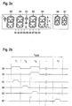
- Figure 2a shows the light segments of a VFD or an LED display. With a designated segments are interconnected in parallel and with the connector S1 connected, the elements labeled b to the terminal S2, etc.
- the connections G1 to G7 are each with a number (possibly connected with adjacent symbols) extending grid.
- the control for an LED display is basically the same as straight described, only that a negative instead of a positive at the connections S1 to S9 Voltage is present.
- the display elements of an LCD are shown in FIG. 3a. Up to three of each Display elements are interconnected in parallel and to connections S1 connected up to S13. The back electrodes of the three elements are each on the Connection COM 1, COM 2 or COM 3 connected.
- FIG 3b is the time course of the connections COM 1, COM 2 and COM 3 as well as signals present at connection S12, where it is a standard procedure for controlling an LCD.
- the Andes Connections S1 to S13 are compared to the signals at COM 1, COM 2 and COM 3 signals present in opposite polarity, so that e.g. on the upper display element S12 a voltage corresponding to COM 1 minus S12 is present, on the middle display element S12 corresponding to COM 2 minus S12 and on the lower display element S12 corresponding to COM 3 minus S12.
- the Voltage differences, which on the upper display element (accordingly COM 1 minus S12) are too small for the crystals to align could. There is therefore no display there. In the middle and lower Display element, however, large voltage differences of 2 U occur, which is why here an alignment of the crystals and thus an indication is given.
- FIG. 4 now shows a basic circuit diagram of the driver elements 11.1 to 11.16 each included circuitry for generating the control signals for the display 2.
- the control block 8 switches 18 and 19 driven by digital signals W4 and W0.
- a signal i.e. Voltage present
- the switch 18 is closed via a digital signal W4
- the switch 18 is opened and the Switch 19 closed by a digital signal W0.
- the (accordingly dimensioned) switches 18 and 19 for a VFD or LED element suitable signal are generated.
- Switches 19, 20, 21 and 22 are used to control an LCD element. By closing the corresponding switch using the associated, The digital signal W0, W1, W2 or W3 coming from the control block 7 can Voltage at output A can be adjusted to 0, 1/3 U, 2/3 U or U, where U is typically 3.3 V.
- the control logic 5, the memory element 6 and the control blocks 7 and 8 of the Circuit arrangement 1 are implemented digitally, while the driver module 11 is carried out analogously with the driver elements 11.1 to 11.16.
- the whole Circuit arrangement 1 is designed as an integrated circuit (IC). In these IC are also the reset circuit 12, the buzzer circuit 13 and the relay driver 15 integrated.
Landscapes
- Engineering & Computer Science (AREA)
- Physics & Mathematics (AREA)
- Computer Hardware Design (AREA)
- General Physics & Mathematics (AREA)
- Theoretical Computer Science (AREA)
- Chemical & Material Sciences (AREA)
- Crystallography & Structural Chemistry (AREA)
- Control Of Indicators Other Than Cathode Ray Tubes (AREA)
Abstract
Es wird eine Schaltungsanordnung (1) zur Ansteuerung einer VFD-, LED- oder LCD-Anzeige (2) vorgeschlagen, welche mindestens zwei Steuerblöcke (7,8) zur Erzeugung von Steuersignalen für die verschiedenen Anzeigearten aufweist, wobei die Steuersignale der Steuerblöcke von einem gemeinsamen Treiberbaustein (11) verarbeitet werden und der Treiberbaustein entsprechende Ansteuersignale an die Anschlüsse der VFD-, LED- oder LCD-Anzeige (2) weitergibt. <IMAGE>A circuit arrangement (1) for controlling a VFD, LED or LCD display (2) is proposed, which has at least two control blocks (7, 8) for generating control signals for the different display types, the control signals of the control blocks being provided by one common driver module (11) are processed and the driver module passes on corresponding control signals to the connections of the VFD, LED or LCD display (2). <IMAGE>
Description
Die Erfindung betrifft eine Schaltungsanordnung zur Ansteuerung einer VFD-, LED- oder LCD-Anzeige.The invention relates to a circuit arrangement for controlling a VFD, LED or LCD display.
Solche Anzeigen sind z.B. bei elektrischen Kleingeräten weit verbreitet. Sie dienen u.a. zur Anzeige der Uhrzeit oder der Temperatur. Bei elektronischen Herdschaltuhren finden sich auf solchen Anzeigen zusätzlich auch Zeichen für die eingestellte Betriebsart des Herdes oder Backofens oder für sonstige Funktionen wie Alarm- oder Funkempfang. Eine Ziffernanzeige (z.B. für die Uhrzeit) wird hier üblicherweise mittels 7-Segmentanzeige realisiert.Such advertisements are e.g. widely used in small electrical appliances. You serve et al to display the time or temperature. With electronic stove time switches on such displays there are also signs for the set one Operating mode of the stove or oven or for other functions such as Alarm or radio reception. A numerical display (e.g. for the time) appears here usually realized using a 7-segment display.
Die Ansteuerung solcher Anzeigen erfolgt entsprechend der Art der jeweiligen Anzeige (VFD, LED, LCD) jeweils unterschiedlich. Bei einer Vakuumfluoreszenz-Anzeige (VFD) liegt hinter den anzuzeigenden Ziffern eine geheizte Kathode. Die einzelnen, einander entsprechenden Segmente der verschiedenen (7-Segment-)Ziffern sind jeweils parallel miteinander verschaltet und bilden die Anoden. Zwischen den geheizten Kathoden und den als Anoden dienenden Segmenten sind Gitter angebracht, welche sich jeweils über den Bereich einer Ziffer erstrecken. Ein Segment einer bestimmten Ziffer leuchtet dann, wenn sowohl die diesem Segment entsprechende Anode als auch das dieser Ziffer entsprechende Gitter auf positiver Spannung liegen. Über eine Multiplex-Ansteuerung der Segmente und der Ziffern (Digits) ist somit jedes einzelne Segment jeder einzelnen Ziffer getrennt ansteuerbar.Such displays are controlled according to the type of each Display (VFD, LED, LCD) each different. With a vacuum fluorescence display (VFD) is a heated cathode behind the digits to be displayed. The individual, corresponding segments of the different (7-segment) digits are connected in parallel with each other and form the anodes. Between the heated cathodes and the segments serving as anodes are attached grids, which each extend over the area of a digit. A segment of a certain number lights up when both the anode corresponding to this segment as well as the one corresponding to this number Grid is at positive voltage. Via multiplex control of the segments and the digits are therefore each individual segment of each individual Number can be controlled separately.
Bei einer Leuchtdioden-Anzeige (LED) sind die einzelnen Segmente der Ziffern jeweils durch einzelne Leuchtdioden gebildet. Die einzelnen, einander entsprechenden Segmente der verschiedenen Ziffern sind wiederum parallel miteinander verschaltet und bilden die Kathode, während die verschiedenen Ziffern (Digits) die Anoden bilden. Auch hier kann jedes Segment mittels Multiplex-Ansteuerung getrennt angesprochen werden.In the case of a light-emitting diode display (LED), the individual segments are the digits each formed by individual light emitting diodes. The individual, corresponding to each other Segments of the different digits are again parallel to each other interconnects and form the cathode, while the various digits form the anodes. Here too, each segment can be controlled by means of multiplex can be addressed separately.
Der Unterschied in der Ansteuerung zwischen VFD- und LED-Anzeige besteht zum einen darin, daß beim VFD an die Anschlüsse entweder positive Spannung oder keine Spannung angelegt wird, während an die Anschlüsse der LED-Anzeige positive (für Ziffern) bzw. negative (bei Segmenten) oder keine Spannung angelegt wird. Zum anderen wird ein VFD mit einer relativ hohen Spannung von 16 bis 30 V, aber geringem Strom von 0,1 bis 2 mA betrieben, während eine LED-Anzeige nur eine kleine Spannung von etwa 2 V, aber einen größeren Strom von 2 bis 20 mA benötigt.The difference in the control between VFD and LED display is on the one hand in that the VFD has either positive voltage at the connections or no voltage is applied while on the connections of the LED display positive (for digits) or negative (for segments) or no voltage applied becomes. Second, a VFD with a relatively high voltage of 16 operated up to 30 V, but low current of 0.1 to 2 mA, while an LED display only a small voltage of about 2 V, but a larger current of 2 up to 20 mA required.
Die Ansteuerung einer Flüssigkristall-Anzeige (LCD) erfolgt dagegen grundlegend anders. Hier handelt es sich um passive Elemente, welche auf einem das Umgebungslicht zurückstreuenden Untergrund aufgebracht sind. Wird an ein solches Element eine elektrische Spannung angelegt, richten sich die in ihm enthaltenen Kristalle aus, wodurch das Umgebungslicht an dieser Stelle absorbiert wird, weshalb das Element dunkel erscheint. Um diesen Effekt längere Zeit aufrecht zu erhalten, muß das Element allerdings immer wieder (etwa alle 100 ms) umgeladen werden. Die Spannung, die dabei an das Element angelegt wird, muß einen bestimmten Mindestwert überschreiten, um eine Ausrichtung der Kristalle zu bewirken.The control of a liquid crystal display (LCD), however, is fundamentally different. These are passive elements which are based on the Ambient light scattering background are applied. Will such a Element applied an electrical voltage, the contained in it Crystals, which absorbs the ambient light at this point, which is why the element appears dark. To sustain this effect for a long time received, the element must be reloaded again and again (approximately every 100 ms) become. The voltage that is applied to the element must be certain Exceed the minimum value in order to align the crystals.
Ein LCD ist nun derart aufgebaut, daß bis zu 3 Segmente miteinander parallel
verschaltet sind und so die eine Elektrode bilden. Die andere Elektrode wird durch
drei Rückelektroden (COM) gebildet, welche jeweils einem der drei miteinander
parallel verschalteten Segmente zugeordnet sind. Auf diese Weise ist auch hier
wieder eine Multiplex-Ansteuerung möglich. Allerdings liegen hier an den einzelnen
Anschlüssen der Anzeige nicht nur zwei Spannungswerte (positiv bzw. negativ
und Null), sondern auch Spannungszwischenwerte (im beschriebenen Fall 1/3
und 2/3 der Spannung) an, damit ein gezieltes Umladen einzelner Elemente ohne
Beeinflussung der anderen Elemente möglich ist. An LCD is now constructed in such a way that up to 3 segments are parallel to each other
are connected and thus form an electrode. The other electrode is through
three back electrodes (COM) formed, each one of the three with each other
parallel connected segments are assigned. This way is also here
Multiplex control possible again. However, here are up to the individual
Connections of the display not only two voltage values (positive or negative
and zero), but also intermediate voltage values (in the described
Während die Ansteuerung eines VFD und einer LED-Anzeige ähnlich erfolgt und bei genügend großzügiger Dimensionierung der Bauteile mit einer Ansteuerschaltung bewerkstelligbar ist, ist für die Ansteuerung eines LCD eine grundsätzlich andere Ansteuerschaltung notwendig. Andererseits wäre es jedoch wünschenswert, eine einzige Ansteuerschaltung zu haben, welche flexibel für VFD-, LED- und LCD-Anzeigen geeignet ist. Dies würde eine erhöhte Bauteilstandardisierung, eine Reduzierung des Aufwandes für Logistik und Lagerhaltung sowie eine flexiblere Reaktion auf Kundenwünsche zur Folge haben.While the control of a VFD and an LED display is similar and with sufficiently large dimensioning of the components with a control circuit is feasible, is essential for driving an LCD other control circuit necessary. On the other hand, it would be desirable to have a single control circuit that is flexible for VFD, LED and LCD displays are suitable. This would result in increased component standardization, a reduction in the effort for logistics and warehousing as well result in a more flexible response to customer requests.
Daher ist es Aufgabe der vorliegenden Erfindung, ausgehend von dem aufgezeigten Stand der Technik eine Ansteuerschaltung zu schaffen, welche sowohl eine VFD- und LED- als auch eine LCD-Anzeige anzusteuern in der Lage ist.It is therefore an object of the present invention, starting from that shown State of the art to create a control circuit which both VFD and LED as well as an LCD display is able to control.
Diese Aufgabe wird durch eine Schaltungsanordnung mit den Merkmalen des
Patentanspruchs 1 erfüllt. Die Patentansprüche 2 bis 8 beschreiben Ausführungsformen
und Weiterbildungen der Erfindung.This object is achieved by a circuit arrangement with the features of
Die Fähigkeit, eine VFD-, LED- und LCD-Anzeige anzusteuern, wird dadurch erreicht, daß mindestens zwei Steuerblöcke vorgesehen sind, wobei einer der Steuerblöcke die für eine LCD-Anzeige notwendigen Steuersignale erzeugt und der andere die für eine VFD- oder LED- oder für beide Anzeigen notwendigen Steuersignale erzeugt. Die Steuersignale der Steuerblöcke werden einem gemeinsamen Treiberbaustein zugeführt, der aus diesen Steuersignalen entsprechende Ansteuersignale für die VFD-/LED-Anzeige und für die LCD-Anzeige erzeugt und an die entsprechende Anzeige weitergibt.The ability to drive a VFD, LED and LCD display is thereby achieved that at least two control blocks are provided, one of the Control blocks generates the control signals necessary for an LCD display and the other the one necessary for a VFD or LED or for both displays Control signals generated. The control signals of the control blocks become common Driver module supplied, the corresponding from these control signals Control signals for the VFD / LED display and for the LCD display are generated and passes it on to the corresponding ad.
In Weiterbildung der Erfindung sind drei Steuerblöcke vorgesehen, von denen jeweils einer für die LCD-, die VFD- und die LED-Anzeige die nötigen Steuersignale liefert.In a further development of the invention, three control blocks are provided, one of which one each for the LCD, VFD and LED displays the necessary control signals supplies.
Des weiteren können ein oder mehrere Speicherelemente vorgesehen sein, die jeweils den einzelnen Steuerblöcken zugeordnet sind. Furthermore, one or more storage elements can be provided are assigned to the individual control blocks.
In Ausgestaltung der Erfindung weist der Treiberbaustein mehrere Treiberelemente auf, von denen jedes mit jeweils einem Anschluß der VFD-, LED- oder LCD-Anzeige verbunden ist und diesem Anschluß ein entsprechendes Ansteuersignal zuführt.In one embodiment of the invention, the driver module has several driver elements on, each with a connection of the VFD, LED or LCD display is connected and this connection a corresponding control signal supplies.
Weiterhin ist bevorzugt vorgesehen, daß jedes Treiberelement mit jedem der Steuerblöcke verbunden ist, so daß ihm alle für die Ansteuerung des Anschlusses der angeschlossenen Anzeige nötigen Steuersignale zugeführt werden.Furthermore, it is preferably provided that each driver element with each of the Control blocks is connected so that it is all used to control the connection necessary control signals are supplied to the connected display.
Bevorzugt sind die Steuersignale der Steuerblöcke in den Treiberelementen derart verschaltet, daß dem Anschluß der angeschlossenen Anzeige das jeweils passende Ansteuersignal zugeführt wird. Diese Verschaltung erfolgt in Weiterbildung der Erfindung in Abhängigkeit der Art der angeschlossenen Anzeige.The control signals of the control blocks in the driver elements are preferably such interconnects that the connection of the connected display the appropriate one Control signal is supplied. This interconnection takes place in a further development of Invention depending on the type of display connected.
Bevorzugt sind die Steuerlogik, das mindestens eine Speicherelement und die Steuerblöcke digital ausgeführt, während der Treiberbaustein analog ausgeführt ist.The control logic, the at least one memory element and the Control blocks executed digitally, while the driver block executed analog is.
Im folgenden soll anhand der Zeichnung eine Ausführungsform der Erfindung näher erläutert werden. Es zeigen:
Figur 1- ein Blockschaltbild einer erfindungsgemäßen Schaltungsanordnung,
- Figur 2a
- die Anzeige eines VFD- bzw. LED-Displays,
- Figur 2b
- den zeitlichen Verlauf der Ansteuersignale für ein VFD- bzw. LED-Display,
- Figur 3a
- die Anzeige eines LCD,
- Figur 3b
- den zeitlichen Verlauf der Ansteuersignale eines LCD und
Figur 4- den prinzipiellen Schaltungsaufbau eines Treiberelementes.
- Figure 1
- 2 shows a block diagram of a circuit arrangement according to the invention,
- Figure 2a
- the display of a VFD or LED display,
- Figure 2b
- the time course of the control signals for a VFD or LED display,
- Figure 3a
- the display of an LCD,
- Figure 3b
- the time course of the control signals of an LCD and
- Figure 4
- the basic circuit structure of a driver element.
Eine Schaltungsanordnung 1 zur Ansteuerung einer VFD-, LED- oder LCD-Anzeige
2 weist einen Datenempfänger 3 auf, welcher für die Ansteuerung der
Anzeige nötige Daten von einem Mikroprozessor 4 empfängt, welcher den Datenempfänger
3 gleichzeitig mit einer Uhrzeit 4.1 versorgt. Der Datenempfänger 3
gibt die empfangenen Daten an eine Steuerlogik 5 weiter. Die Steuerlogik 5 überprüft
die empfangenen Daten und dekodiert sie, indem sie aus den empfangenen
Daten Adressen, Steuerwörter und Befehle extrahiert. Die Befehle enthalten die
eigentlichen Anzeigedaten. Diese Anzeigedaten werden an einen Datenspeicher 6
weitergegeben und dort gespeichert. Sie bleiben so lange unverändert gespeichert,
bis die Anzeige verändert werden soll. Dann werden neue Anzeigedaten in dem
Datenspeicher 6 gespeichert.A
Weiterhin teilt die Steuerlogik 5 einem ersten Steuerblock 7, welcher der Erzeugung
von für eine LCD-Anzeige nötigen Steuersignalen dient, und einem zweiten
Steuerblock 8, welcher der Erzeugung von für eine VFD- bzw. LED-Anzeige nötigen
Steuersignale dient, mit, welcher Ansteuerungsmodus eingestellt ist (z.B.
VFD/LED 5fach, 6fach oder 7fach Multiplex, LCD 3fach Multiplex, Nachtabsenkung
oder Lastabwurf; siehe unten). Der gewählte Modus ist in dem ROM-Block
9 gespeichert, welcher mit der Steuerlogik 5 in Wirkverbindung steht.Furthermore, the
Je nachdem, ob ein LCD- oder VFD/LED-Modus eingestellt ist, wird der Steuerblock
7 oder der Steuerblock 8 aktiv. Anhand der ihm von dem Datenspeicher 6
bereitgestellten Anzeigedaten erzeugt der aktive Steuerblock 7 bzw. 8 in üblicher
und weiter unten noch näher erläuterter Weise die für die jeweilige Anzeige 2
nötigen Steuersignale COM 1 bis 3 und S 1 bis 13 (LCD) bzw. G 1 bis 7 und S 1
bis 9 (VFD/LED) (siehe auch weiter unten).Depending on whether an LCD or VFD / LED mode is set, the
Die Steuersignale aus dem Steuerblock 8 durchlaufen noch den Pegel-Verschieber
10, in welchem bei Vorliegen eines VFD-Modus die Pegel der Steuersignale von
üblichen 3,3 V auf für ein VFD notwendige 30 V angehoben werden. Im Falle
eines LED-Modus ist diese Pegelerhöhung nicht notwendig. Die Information über
den eingestellten Modus erhält der Pegel-Verschieber 10 ebenso wie die Steuerblöcke
7 und 8 von der Steuerlogik 5. The control signals from the
Die Steuersignale der Steuerblöcke 7 und 8 gelangen sodann zum Treiberbaustein
11. Dieser weist einzelne Treiberelemente 11.1 bis 11.16 auf. Diese empfangen
die jeweiligen Steuersignale des Steuerblocks 7 oder 8, verarbeiten diese und geben
sie in für die Anzeige 2 geeigneter Form an diese weiter. Dabei ist jedes der
Treiberelemente 11.1 bis 11.16 mit jeweils einem Anschluß der Anzeige 2 verbunden.The control signals of the control blocks 7 and 8 then arrive at the
Alternativ ist es auch möglich, daß beide Steuerblöcke 7 und 8 unabhängig vom
eingestellten Modus jederzeit aktiv sind. In diesem Fall ist es jedoch notwendig,
daß die Treiberelemente 11.1 bis 11.16 Steuersignale je nach eingestelltem Modus
(LCD oder VFD/LED) nur von einem der Steuerblöcke 7 und 8 empfangen. Die
entsprechende Information erhalten die Treiberelemente 11.1 bis 11.16 direkt von
der Steuerlogik 5.Alternatively, it is also possible for both
Weiterhin steuert die Steuerlogik 5 noch eine Reset-Schaltung 12 für den Mikroprozessor
4, eine Summerschaltung 13 für einen Summer 14 sowie einen Treiber
15 zur Ansteuerung von Relais 16 und 17. Darüber hinaus sei noch bemerkt, daß
eine Spannungsversorgung für die einzelnen Bauteile der Schaltungsanordnung 1
der Übersichtlichkeit halber nicht gezeichnet ist; die Spannungsversorgung erfolgt
jedoch in üblicher Art und Weise.The
Figur 2a zeigt die Leuchtsegmente eines VFD- bzw. eines LED-Displays. Die mit a bezeichneten Segmente sind miteinander parallel verschaltet und mit dem Anschluß S1 verbunden, die mit b bezeichneten Elemente mit dem Anschluß S2 usw. Die Anschlüsse G1 bis G7 sind jeweils mit dem sich über eine Ziffer (eventuell mit danebenstehenden Symbolen) erstreckenden Gitter verbunden.Figure 2a shows the light segments of a VFD or an LED display. With a designated segments are interconnected in parallel and with the connector S1 connected, the elements labeled b to the terminal S2, etc. The connections G1 to G7 are each with a number (possibly connected with adjacent symbols) extending grid.
Die Ansteuerung einer solchen Anzeige soll nun anhand von Figur 2b erläutert werden, in welcher der zeitliche Verlauf der an den Anschlüssen S1 bis S9 und G1 bis G7 anliegenden Signale in Auszügen dargestellt ist. Während der Zeitspanne t1 liegt sowohl am Anschluß S1 als auch am Anschluß G1 ein Signal, d.h. Spannung an. Damit leuchtet das Segment a derjenigen Ziffer auf, welche zu dem an Anschluß G1 angeschlossenen Gitter gehört. In der Zeitspanne t2 wird das zum Anschluß G2 gehörige Gitter angesteuert, jedoch werden hier keine Segmente angesteuert, so daß die zu G2 gehörige Ziffer dunkel bleibt. Die zum an G3 angeschlossenen Gitter gehörigen Symbole a und b leuchten jedoch wieder, da an den Anschlüssen S1 und S2 während der Zeitspanne t3 jeweils ein Signal anliegt.The control of such a display will now be explained with reference to Figure 2b in which the time profile of the connections S1 to S9 and G1 Excerpts of signals applied to G7 are shown. During the period t1 there is a signal at both terminals S1 and G1, i.e. tension on. This illuminates segment a of the digit that corresponds to that Connection G1 belongs to the connected grid. In the period t2 this becomes Connection G2 associated grids driven, but no segments are here controlled so that the digit belonging to G2 remains dark. Those connected to G3 Symbols a and b belonging to the grid light up again, however, because of the Connections S1 and S2 each have a signal during the time period t3.
Im vorliegenden Fall werden sieben Gitter angesteuert, so daß sich die Zyklusdauer aus den Zeitspannen t1 bis t7 zusammensetzt. Es handelt sich hierbei somit um einen 7fachen Multiplex. Bei Wegfall der zu G6 und G7 gehörenden Gitter würde sich die Zyklusdauer entsprechend verringern, es wäre dann ein 5facher Multiplex gegeben.In the present case, seven grids are controlled, so that the cycle time composed of the time periods t1 to t7. It is thus here by a 7-fold multiplex. If the grids belonging to G6 and G7 are omitted the cycle time would decrease accordingly, it would then be 5 times Given multiplex.
Die Ansteuerung für eine LED-Anzeige verläuft grundsätzlich ebenso wie gerade beschrieben, nur daß an den Anschlüssen S1 bis S9 statt einer positiven eine negative Spannung anliegt.The control for an LED display is basically the same as straight described, only that a negative instead of a positive at the connections S1 to S9 Voltage is present.
In Figur 3a sind die Anzeigeelemente eines LCD gezeigt. Jeweils bis zu drei der
Anzeigeelemente sind miteinander parallel verschaltet und an die Anschlüsse S1
bis S13 angeschlossen. Die Rückelektroden der drei Elemente sind jeweils an den
Anschluß COM 1, COM 2 oder COM 3 angeschlossen.The display elements of an LCD are shown in FIG. 3a. Up to three of each
Display elements are interconnected in parallel and to connections S1
connected up to S13. The back electrodes of the three elements are each on the
In Figur 3b ist der zeitliche Verlauf der an den Anschlüssen COM 1, COM 2 und
COM 3 sowie an dem Anschluß S12 anliegenden Signale dargestellt, wobei es
sich um ein Standardverfahren zur Ansteuerung eines LCD handelt. Die an den
Anschlüssen S1 bis S13 anliegenden Signale sind gegenüber den an COM 1,
COM 2 und COM 3 anliegenden Signalen entgegengesetzt gepolt, so daß z.B. an
dem oberen Anzeigeelement S12 eine Spannung entsprechend COM 1 minus S12
anliegt, an dem mittleren Anzeigeelement S12 entsprechend COM 2 minus S12
und an dem unteren Anzeigeelement S12 entsprechend COM 3 minus S12. Die
Spannungsdifferenzen, welche an dem oberen Anzeigeelement (entsprechend
COM 1 minus S12) auftreten, sind zu gering, als daß sich die Kristalle ausrichten
könnten. Dort findet somit keine Anzeige statt. Bei dem mittleren und unteren
Anzeigeelement jedoch treten große Spannungsdifferenzen von 2 U auf, weshalb
hier eine Ausrichtung der Kristalle und damit eine Anzeige erfolgt. In Figure 3b is the time course of the
Figur 4 zeigt nun ein Prinzipschaltbild der in den Treiberelementen 11.1 bis 11.16
jeweils enthaltenen Verschaltung zur Erzeugung der Ansteuersignale für die Anzeige
2. Im VFD- bzw. LED-Mode werden vom Steuerblock 8 die Schalter 18 und
19 mittels digitaler Signale W4 und W0 angesteuert. Soll am Ausgang A, d.h. am
entsprechenden Anschluß der Anzeige 2, ein Signal, d.h. Spannung anliegen, so
wird über ein digitales Signal W4 der Schalter 18 geschlossen, während der
Schalter 19 wie auch die Schalter 20, 21 und 22 geöffnet bleiben. Bei Verwendung
einer VFD-Anzeige beträgt die nun am Ausgang A anliegende Spannung U'
30 V, bei Verwendung einer LED-Anzeige lediglich etwa 2 V. Soll am Ausgang
kein Signal, also keine Spannung anliegen, wird der Schalter 18 geöffnet und der
Schalter 19 durch ein digitales Signal W0 geschlossen. Somit kann über die (entsprechend
dimensionierten) Schalter 18 und 19 ein für ein VFD- bzw. LED-Element
geeignetes Signal erzeugt werden. Die Information, ob eine Spannung U'
von 30 V oder lediglich von 2 V Verwendung findet (entsprechend der Steuerung
eines VFD oder einer LED-Anzeige), kann das jeweilige Treiberelement 11.1 bis
11.16 entweder vom Pegel-Verschieber 10 oder von der Steuerlogik 5 direkt erhalten
(siehe Figur 1).FIG. 4 now shows a basic circuit diagram of the driver elements 11.1 to 11.16
each included circuitry for generating the control signals for the
Zur Steuerung eines LCD-Elementes werden die Schalter 19, 20, 21 und 22 verwendet.
Durch Schließen des entsprechenden Schalters mittels des zugehörigen,
vom Steuerblock 7 kommenden digitalen Signals W0, W1, W2 oder W3 kann die
Spannung am Ausgang A auf 0, 1/3 U, 2/3 U oder U eingeregelt werden, wobei U
typischerweise 3,3 V beträgt.
Auf diese Weise kann durch Ansteuerung der geeigneten Schalter durch die von den Steuerblöcken 7 und 8 kommenden digitalen Signale W0, W1, W2, W3 und W4 über ein- und denselben Ausgang bzw. Anschluß A sowohl ein LCD- als auch ein VFD- und LED-Element angesteuert werden.In this way, by controlling the appropriate switch by the the control blocks 7 and 8 coming digital signals W0, W1, W2, W3 and W4 via one and the same output or connection A both an LCD and a VFD and LED element can be controlled.
Die Steuerlogik 5, das Speicherelement 6 und die Steuerblöcke 7 und 8 der
Schaltungsanordnung 1 sind digital ausgeführt, während der Treiberbaustein 11
mit den Treiberelementen 11.1 bis 11.16 analog ausgeführt ist. Die gesamte
Schaltungsanordnung 1 ist als integrierter Schaltkreis (IC) ausgeführt. In diesen
IC sind auch die Reset-Schaltung 12, die Summerschaltung 13 und der Relais-Treiber
15 integriert.The
Claims (8)
mit einem Datenempfänger (3), der die für die Ansteuerung der Anzeige (2) nötigen Daten von einer Zentraleinheit (4) empfängt,
mit einer Steuerlogik (5), welche die von dem Datenempfänger (3) empfangenen Daten überprüft und aus ihnen Anzeigedaten extrahiert,
mit mindestens einem Speicherelement (6), in dem die jeweils aktuellen Anzeigedaten gespeichert werden,
mit mindestens zwei Steuerblöcken (7,8), die mit dem mindestens einen Speicherelement (6) in Datenverbindung stehen, zur Erzeugung der für die Anzeige notwendigen Steuersignale in Abhängigkeit der in dem mindestens einen Speicherelement (6) gespeicherten Anzeigedaten,
wobei der erste Steuerblock (7) derart ausgebildet ist, daß er die für eine LCD-Anzeige nötigen Steuersignale liefert,
und der zweite Steuerblock (8) derart ausgebildet ist, daß er die für eine VFD- oder eine LED- oder sowohl für eine VFD- als auch für eine LED-Anzeige nötigen Steuersignale liefert,
und mit einem gemeinsamen Treiberbaustein (11), dem die Steuersignale der Steuerblöcke (7) und (8) zugeführt werden, der aus diesen Steuersignalen entsprechende Ansteuersignale für die VFD-, LED- und/oder LCD-Anzeigen erzeugt und diese an die entsprechende Anzeige (2) weitergibt.Circuit arrangement (1) for controlling a VFD, LED or LCD display (2)
with a data receiver (3) which receives the data necessary for controlling the display (2) from a central unit (4),
with control logic (5) which checks the data received by the data receiver (3) and extracts display data from them,
with at least one storage element (6) in which the current display data is stored,
with at least two control blocks (7, 8), which are in data connection with the at least one memory element (6), for generating the control signals necessary for the display as a function of the display data stored in the at least one memory element (6),
the first control block (7) being designed in such a way that it supplies the control signals necessary for an LCD display,
and the second control block (8) is designed such that it supplies the control signals necessary for a VFD or an LED or both for a VFD and for an LED display,
and with a common driver module (11), to which the control signals of the control blocks (7) and (8) are fed, which generates corresponding control signals for the VFD, LED and / or LCD displays from these control signals and these to the corresponding display (2) passes on.
dadurch gekennzeichnet, daß drei Steuerblöcke vorgesehen sind, wobei der erste die für die LCD-Anzeige, der zweite die für die VFD-Anzeige und der dritte die für die LED-Anzeige nötigen Steuersignale liefert. Circuit arrangement according to claim 1,
characterized in that three control blocks are provided, the first supplying the control signals necessary for the LCD display, the second supplying the VFD display and the third the control signals required for the LED display.
dadurch gekennzeichnet, daß mehrere Speicherelemente (6) vorgesehen sind, die jeweils den LCDund dem VFD-/LED-Steuerblock (7,8) bzw. dem LCD-, dem VFD- und dem LED-Steuerblock zugeordnet sind.Circuit arrangement according to claim 1 or 2,
characterized in that a plurality of memory elements (6) are provided, each of which is assigned to the LCD and the VFD / LED control block (7, 8) or to the LCD, the VFD and the LED control block.
dadurch gekennzeichnet, daß der Treiberbaustein (11) mehrere Treiberelemente (11.1-11.16) aufweist, wobei jedes Treiberelement (11.1-11.16) mit jeweils einem Anschluß der VFD-, LED- oder LCD-Anzeige (2) verbunden ist und diesem Anschluß das entsprechende Ansteuersignal zuführt.Circuit arrangement according to one of claims 1 to 3,
characterized in that the driver module (11) has a plurality of driver elements (11.1-11.16), each driver element (11.1-11.16) being connected to a respective connector of the VFD, LED or LCD display (2) and this connector the corresponding one Control signal feeds.
dadurch gekennzeichnet, daß jedes Treiberelement (11.1-11.16) derart mit jedem der Steuerblöcke (7,8) verbunden ist, daß es die für die Ansteuerung des einen Anschlusses der VFD-, LED- oder LCD-Anzeige (2) nötigen Steuersignale zugeführt bekommt.Circuit arrangement according to claim 4,
characterized in that each driver element (11.1-11.16) is connected to each of the control blocks (7, 8) in such a way that it receives the control signals necessary for controlling the one connection of the VFD, LED or LCD display (2) ,
dadurch gekennzeichnet, daß die Steuersignale der Steuerblöcke (7,8) in den Treiberelementen (11.1-11.16) derart verschaltet sind, daß dem Anschluß der VFD-, LED- oder LCD-Anzeige (2) das passende Ansteuersignal zugeführt wird.Circuit arrangement according to claim 5,
characterized in that the control signals of the control blocks (7, 8) in the driver elements (11.1-11.16) are connected in such a way that the appropriate control signal is supplied to the connection of the VFD, LED or LCD display (2).
dadurch gekennzeichnet, daß die Verschaltung der Steuersignale in den Treiberelementen (11.1-11.16) in Abhängigkeit der Art der angeschlossenen Anzeige (2) erfolgt. Circuit arrangement according to claim 6,
characterized in that the control signals are interconnected in the driver elements (11.1-11.16) depending on the type of display (2) connected.
dadurch gekennzeichnet, daß die Steuerlogik (5), das mindestens eine Speicherelement (6) und die Steuerblöcke (7,8) digital arbeitend ausgeführt sind, während der Treiberbaustein (11) analog arbeitend ausgeführt ist.Circuit arrangement according to one of the preceding claims,
characterized in that the control logic (5), the at least one memory element (6) and the control blocks (7, 8) are designed to work digitally, while the driver module (11) is designed to work in an analog manner.
Applications Claiming Priority (2)
| Application Number | Priority Date | Filing Date | Title |
|---|---|---|---|
| DE10109157 | 2001-02-24 | ||
| DE10109157A DE10109157A1 (en) | 2001-02-24 | 2001-02-24 | Circuit arrangement for driving a display |
Publications (2)
| Publication Number | Publication Date |
|---|---|
| EP1237140A1 true EP1237140A1 (en) | 2002-09-04 |
| EP1237140B1 EP1237140B1 (en) | 2005-11-02 |
Family
ID=7675500
Family Applications (1)
| Application Number | Title | Priority Date | Filing Date |
|---|---|---|---|
| EP02003965A Expired - Lifetime EP1237140B1 (en) | 2001-02-24 | 2002-02-22 | Circuit for driving a display |
Country Status (4)
| Country | Link |
|---|---|
| US (1) | US6844864B2 (en) |
| EP (1) | EP1237140B1 (en) |
| DE (2) | DE10109157A1 (en) |
| PL (1) | PL198894B1 (en) |
Cited By (1)
| Publication number | Priority date | Publication date | Assignee | Title |
|---|---|---|---|---|
| US6025921A (en) * | 1995-01-23 | 2000-02-15 | Ohio Electronics Engravers, Inc. | Method and apparatus for engraving a mixed pattern |
Families Citing this family (3)
| Publication number | Priority date | Publication date | Assignee | Title |
|---|---|---|---|---|
| US7109957B2 (en) * | 1999-01-22 | 2006-09-19 | Au Optronics Corp. | Digital display driving circuit for light emitting diode display |
| DE10225996B4 (en) * | 2002-06-12 | 2006-01-12 | Diehl Ako Stiftung & Co. Kg | Control circuit for a vacuum fluorescent display |
| US7970439B2 (en) * | 2005-03-01 | 2011-06-28 | Kyocera Corporation | Systems and methods for visual alerting mechanisms on a mobile communication device |
Family Cites Families (17)
| Publication number | Priority date | Publication date | Assignee | Title |
|---|---|---|---|---|
| US3984973A (en) * | 1973-10-29 | 1976-10-12 | Hughes Aircraft Company | Digital watch with liquid crystal and light emitting diode displays |
| JPS5665537A (en) * | 1979-11-01 | 1981-06-03 | Nec Corp | Individual selection callout receiver with display |
| JPS56162588U (en) | 1980-04-30 | 1981-12-03 | ||
| GB2075726B (en) | 1980-05-02 | 1983-11-23 | Suwa Seikosha Kk | Electronic timepiece |
| JPS58162988A (en) * | 1982-03-23 | 1983-09-27 | 日本電気株式会社 | Display |
| US4542799A (en) * | 1982-04-28 | 1985-09-24 | Shimadzu Corporation | Display device for use in an electronic balance |
| JPS5991487A (en) * | 1982-11-17 | 1984-05-26 | 富士通株式会社 | Display unit |
| JPS60227296A (en) | 1984-04-25 | 1985-11-12 | シャープ株式会社 | Display control method |
| JPS61213896A (en) * | 1985-03-19 | 1986-09-22 | 株式会社 アスキ− | Display controller |
| JPS6347791A (en) * | 1986-08-15 | 1988-02-29 | 株式会社東芝 | Information display instructor |
| JPH01248186A (en) * | 1988-03-30 | 1989-10-03 | Toshiba Corp | Display attribute converting device |
| US5021775A (en) * | 1989-02-27 | 1991-06-04 | Motorola, Inc. | Synchronization method and circuit for display drivers |
| JP2722824B2 (en) * | 1991-01-30 | 1998-03-09 | 日本電気株式会社 | Display method of day and time |
| JPH0519747A (en) * | 1991-07-09 | 1993-01-29 | Toshiba Corp | Display controller |
| EP0692161A4 (en) * | 1993-03-19 | 1996-04-10 | Motorola Inc | Lcd system with integrated annunciator |
| US5694141A (en) * | 1995-06-07 | 1997-12-02 | Seiko Epson Corporation | Computer system with double simultaneous displays showing differing display images |
| US20030214458A1 (en) * | 2002-05-20 | 2003-11-20 | Vladimir Giemborek | Multiple display configuration |
-
2001
- 2001-02-24 DE DE10109157A patent/DE10109157A1/en not_active Withdrawn
-
2002
- 2002-01-29 US US10/061,055 patent/US6844864B2/en not_active Expired - Fee Related
- 2002-02-22 PL PL352426A patent/PL198894B1/en unknown
- 2002-02-22 EP EP02003965A patent/EP1237140B1/en not_active Expired - Lifetime
- 2002-02-22 DE DE50204737T patent/DE50204737D1/en not_active Expired - Fee Related
Non-Patent Citations (3)
| Title |
|---|
| "1/4 to 1/11-duty fiptm (vfd) controller/driver", NEC DATA SHEET MOS INTEGRATED CIRCUIT UPD16312, XX, XX, 1 March 1997 (1997-03-01), XX, pages 1 - 20, XP002198522 * |
| "oki semiconductor msm9006-01, -02 lcd driver with keyscan function", FEDL9006-03, XX, XX, 1 April 2000 (2000-04-01), XX, pages 1 - 19, XP002198521 * |
| S11543EJ2V0DS00, "Data Sheet µPD6320/µPD6321, FIP/LCD static display driver", October 1996, NEC Corporation * |
Cited By (1)
| Publication number | Priority date | Publication date | Assignee | Title |
|---|---|---|---|---|
| US6025921A (en) * | 1995-01-23 | 2000-02-15 | Ohio Electronics Engravers, Inc. | Method and apparatus for engraving a mixed pattern |
Also Published As
| Publication number | Publication date |
|---|---|
| US6844864B2 (en) | 2005-01-18 |
| EP1237140B1 (en) | 2005-11-02 |
| DE50204737D1 (en) | 2005-12-08 |
| DE10109157A1 (en) | 2002-09-26 |
| PL198894B1 (en) | 2008-07-31 |
| US20020118155A1 (en) | 2002-08-29 |
Similar Documents
| Publication | Publication Date | Title |
|---|---|---|
| DE69914302T2 (en) | ELECTROLUMINESCENT DISPLAY DEVICES WITH ACTIVE MATRIX | |
| DE3634686C2 (en) | ||
| DE60305872T2 (en) | Light-emitting display, display panel and method of their control | |
| DE60110664T2 (en) | Active control circuit for display fields | |
| DE60308641T2 (en) | Light-emitting display, display panel and method of controlling them | |
| DE3019832C2 (en) | Driver circuit for a liquid crystal display matrix | |
| DE69529592T2 (en) | AC CURRENT DRIVE CIRCUIT | |
| DE2810478C2 (en) | ||
| DE3782858T2 (en) | CONTROL FOR A DISPLAY DEVICE IN MATRIX FORM. | |
| DE60219325T2 (en) | METHOD AND DEVICE FOR GAMMA CORRECTION | |
| DE3526321C2 (en) | ||
| DE60204850T2 (en) | PROGRAMMABLE CHARGE PUMP ELEMENT | |
| DE2423675C3 (en) | Device for controlling a capacitive electro-optical display element | |
| DE2513451A1 (en) | ELECTRONIC CLOCK CALCULATOR UNIT | |
| DE2643455A1 (en) | ELECTRONIC CLOCK | |
| DE3433474C2 (en) | ||
| DE19840930A1 (en) | Digital / analog converter, driver circuit for liquid crystal displays and method for converting a digital signal into an analog signal | |
| DE2255913A1 (en) | LIQUID CRYSTAL DISPLAY UNIT AND CONTROL AND SWITCHING DEVICE FOR ITS OPERATION | |
| DE102006026661A1 (en) | Solar module for a photovoltaic system | |
| DE3431299C2 (en) | ||
| EP1237140A1 (en) | Circuit for driving a display | |
| DE2311508C3 (en) | Electro-optical displays for electronic clocks | |
| DE2365143A1 (en) | ELECTRONIC CLOCK | |
| DE69734814T2 (en) | LCD CONTROL UPDATING DATA STORED IN A RAM MEMORY | |
| DE2723412A1 (en) | CONSTANT CURRENT CONTROL CIRCUIT FOR ELECTROCHROME SEGMENT DISPLAY DEVICES |
Legal Events
| Date | Code | Title | Description |
|---|---|---|---|
| PUAI | Public reference made under article 153(3) epc to a published international application that has entered the european phase |
Free format text: ORIGINAL CODE: 0009012 |
|
| AK | Designated contracting states |
Kind code of ref document: A1 Designated state(s): AT BE CH CY DE DK ES FI FR GB GR IE IT LI LU MC NL PT SE TR |
|
| AX | Request for extension of the european patent |
Free format text: AL;LT;LV;MK;RO;SI |
|
| 17P | Request for examination filed |
Effective date: 20020710 |
|
| 17Q | First examination report despatched |
Effective date: 20021023 |
|
| AKX | Designation fees paid |
Designated state(s): DE FR IT |
|
| APBN | Date of receipt of notice of appeal recorded |
Free format text: ORIGINAL CODE: EPIDOSNNOA2E |
|
| APBR | Date of receipt of statement of grounds of appeal recorded |
Free format text: ORIGINAL CODE: EPIDOSNNOA3E |
|
| APBV | Interlocutory revision of appeal recorded |
Free format text: ORIGINAL CODE: EPIDOSNIRAPE |
|
| GRAP | Despatch of communication of intention to grant a patent |
Free format text: ORIGINAL CODE: EPIDOSNIGR1 |
|
| GRAS | Grant fee paid |
Free format text: ORIGINAL CODE: EPIDOSNIGR3 |
|
| APAA | Appeal reference recorded |
Free format text: ORIGINAL CODE: EPIDOS REFN |
|
| APBT | Appeal procedure closed |
Free format text: ORIGINAL CODE: EPIDOSNNOA9E |
|
| GRAA | (expected) grant |
Free format text: ORIGINAL CODE: 0009210 |
|
| APAH | Appeal reference modified |
Free format text: ORIGINAL CODE: EPIDOSCREFNO |
|
| AK | Designated contracting states |
Kind code of ref document: B1 Designated state(s): DE FR IT |
|
| REF | Corresponds to: |
Ref document number: 50204737 Country of ref document: DE Date of ref document: 20051208 Kind code of ref document: P |
|
| ET | Fr: translation filed | ||
| PLBE | No opposition filed within time limit |
Free format text: ORIGINAL CODE: 0009261 |
|
| STAA | Information on the status of an ep patent application or granted ep patent |
Free format text: STATUS: NO OPPOSITION FILED WITHIN TIME LIMIT |
|
| 26N | No opposition filed |
Effective date: 20060803 |
|
| PGFP | Annual fee paid to national office [announced via postgrant information from national office to epo] |
Ref country code: IT Payment date: 20080227 Year of fee payment: 7 |
|
| PGFP | Annual fee paid to national office [announced via postgrant information from national office to epo] |
Ref country code: FR Payment date: 20080227 Year of fee payment: 7 |
|
| PGFP | Annual fee paid to national office [announced via postgrant information from national office to epo] |
Ref country code: DE Payment date: 20090422 Year of fee payment: 8 |
|
| REG | Reference to a national code |
Ref country code: FR Ref legal event code: ST Effective date: 20091030 |
|
| PG25 | Lapsed in a contracting state [announced via postgrant information from national office to epo] |
Ref country code: FR Free format text: LAPSE BECAUSE OF NON-PAYMENT OF DUE FEES Effective date: 20090302 |
|
| PG25 | Lapsed in a contracting state [announced via postgrant information from national office to epo] |
Ref country code: DE Free format text: LAPSE BECAUSE OF NON-PAYMENT OF DUE FEES Effective date: 20100901 |
|
| PG25 | Lapsed in a contracting state [announced via postgrant information from national office to epo] |
Ref country code: IT Free format text: LAPSE BECAUSE OF NON-PAYMENT OF DUE FEES Effective date: 20090222 |