EP1231645A2 - Laterales Halbleiterbauelement in Dünnfilm-SOI-Technik - Google Patents
Laterales Halbleiterbauelement in Dünnfilm-SOI-Technik Download PDFInfo
- Publication number
- EP1231645A2 EP1231645A2 EP01129043A EP01129043A EP1231645A2 EP 1231645 A2 EP1231645 A2 EP 1231645A2 EP 01129043 A EP01129043 A EP 01129043A EP 01129043 A EP01129043 A EP 01129043A EP 1231645 A2 EP1231645 A2 EP 1231645A2
- Authority
- EP
- European Patent Office
- Prior art keywords
- semiconductor component
- substrate
- contact
- component according
- lateral
- Prior art date
- Legal status (The legal status is an assumption and is not a legal conclusion. Google has not performed a legal analysis and makes no representation as to the accuracy of the status listed.)
- Granted
Links
Images


Classifications
-
- H—ELECTRICITY
- H10—SEMICONDUCTOR DEVICES; ELECTRIC SOLID-STATE DEVICES NOT OTHERWISE PROVIDED FOR
- H10D—INORGANIC ELECTRIC SEMICONDUCTOR DEVICES
- H10D12/00—Bipolar devices controlled by the field effect, e.g. insulated-gate bipolar transistors [IGBT]
- H10D12/411—Insulated-gate bipolar transistors [IGBT]
-
- H—ELECTRICITY
- H10—SEMICONDUCTOR DEVICES; ELECTRIC SOLID-STATE DEVICES NOT OTHERWISE PROVIDED FOR
- H10D—INORGANIC ELECTRIC SEMICONDUCTOR DEVICES
- H10D8/00—Diodes
-
- H—ELECTRICITY
- H10—SEMICONDUCTOR DEVICES; ELECTRIC SOLID-STATE DEVICES NOT OTHERWISE PROVIDED FOR
- H10D—INORGANIC ELECTRIC SEMICONDUCTOR DEVICES
- H10D12/00—Bipolar devices controlled by the field effect, e.g. insulated-gate bipolar transistors [IGBT]
- H10D12/411—Insulated-gate bipolar transistors [IGBT]
- H10D12/415—Insulated-gate bipolar transistors [IGBT] having edge termination structures
-
- H—ELECTRICITY
- H10—SEMICONDUCTOR DEVICES; ELECTRIC SOLID-STATE DEVICES NOT OTHERWISE PROVIDED FOR
- H10D—INORGANIC ELECTRIC SEMICONDUCTOR DEVICES
- H10D86/00—Integrated devices formed in or on insulating or conducting substrates, e.g. formed in silicon-on-insulator [SOI] substrates or on stainless steel or glass substrates
- H10D86/201—Integrated devices formed in or on insulating or conducting substrates, e.g. formed in silicon-on-insulator [SOI] substrates or on stainless steel or glass substrates the substrates comprising an insulating layer on a semiconductor body, e.g. SOI
Definitions
- the present invention relates to a lateral semiconductor component using thin-film SOI technology, with an insulator layer, which rests on a substrate and is buried below a thin silicon film on which the source or. Anode contact and the drain or cathode contact are attached.
- CMOS circuits Semiconductor components of the type described at the outset have been around for a long time known and are mainly used in the low voltage range, e.g. as CMOS circuits. So far, mostly circuits for harsh working conditions (high temperatures, increased particle radiation or electromagnetic Radiation). The technology described continues to hold up also found in processors and driver circuits.
- these components can be both transistors and are diodes.
- an anode and a cathode contact or a source, a drain and a gate contact intended. Because the position of the anode is functionally related to the source contact of a Transistor corresponds, and the cathode accordingly the drain contact is to be assigned, the respective terms are synonymous in the following used, without thereby restricting the invention to a certain component is intended.
- a buried p-n junction can be used generate in the substrate that the entire circuit from harmful Protects voltages that occur from the bottom of the circuit. On such p-n transition, e.g. by implantation through the silicon film and The buried oxide that can be produced through is also referred to as a shield. It lies on a set throughout the entire structure Potential.
- the circuit only protects the circuit from voltages that act on the circuit from outside.
- the blocking voltages made possible by this are also relatively low in this case because of the voltage reduction is predetermined by the silicon film and the buried insulator.
- the object of the present invention is therefore a lateral semiconductor component of the type described above to create high reverse voltages within of the component allows, but at the same time technologically simple is feasible and economical to manufacture.
- This object is achieved in that the source or anode contact and the drain or cathode contact of the component in each case over separate shield areas within the substrate, with the anode contact is electrically connected to the substrate.
- the contacts are on a thin silicon film, under which the insulator layer is buried.
- the anode or the source and the gate contact of a transistor and the Cathode or the drain contact on two different and against each other floating shield areas.
- the space charge zone is not only in the thin silicon film and degraded in buried oxide, but also in the substrate.
- the advantage of the present semiconductor component is the high blocking capability its structure.
- the back gate effect no longer occurs because that Structured shield area and connected to the anode of each component is. This means that no back gate voltage can be set.
- the invention offers the advantage that several high-voltage switches can be integrated on a chip without special epitaxial layers, Buried insulator oxide thicknesses or certain silicon film thicknesses are necessary. This makes it possible to bridge systems on a chip build and integrate almost any vertical transistor structure.
- everyone Transistor can contain a dielectric isolated logic part so that Entire half and full bridge drivers are manufactured with monitoring electronics to let.
- the two shield areas of the anode and cathode contacts, preferably by one in between arranged buried edge structure isolated from each other.
- this is a floating one Field ring structure.
- floating field rings which are also called field limiting rings (FLR) are referred to, it is a marginal structure principle, at which a blocking p-n transition through upstream field rings, i.e. p-n transitions in tub form, is protected. These rings are not contacted and stand on a potential between maximum and minimum voltage on.
- the buried edge structure can be can also be implemented as a VLE or JTE structure.
- VLE structure variant of material doping
- JTE structure junction termination extension
- the p-n transition which adjoins in the lateral direction, has a deeper one Depth of penetration than the blocking p-n junction. Under certain circumstances, however even the simple p-n transition between the cathode and and the anode contact is arranged.
- the electrical connection of the anode contact to the substrate is preferred produced directly by a metallic contact. In another preferred embodiment, this connection is made by an electrical Component manufactured.
- the drain contact makes electrical contact with the substrate. It is crucial that the shield area is contacted, via which the majority of the reverse voltage drops. Is the blocking p-n transition sufficient contacts and adapts the SOI component to the horizontal Under certain circumstances, a further contacting of the SOI component is possible not mandatory.
- the arrangement may only be operated with positive cathode-anode voltages, the highest potential having to be due to a substrate contact which is attached on the back or in another suitable manner is.
- the cathode shield forms a channel stopper, which closes the structure in the substrate and prevents the space charge from expanding beyond the structure boundary.
- the cathode shield must be of the same doping type as the substrate, but must be doped in the opposite manner with respect to the anode shield. For example, if the substrate is n-doped and the anode shield is p-doped, the channel stopper must be n + -doped.
- the semiconductor component according to the invention a transistor, the source and the gate contact on the one hand and the drain contact, on the other hand, via separate shield areas within the Substrate.
- the semiconductor component is a Diode, a voltage resistant resistor or an IGBT, i.e. an "insulated gate bipolar transistor ".
- a semiconductor circuit with a transistor as the semiconductor component according to the invention it is a level shift transistor, which in a driver circuit with a suitable vertical power component, such as about an IGBT, a DMOS or the like is integrated.
- the semiconductor component according to the invention is a diode is preferably an SOI diode and as a decoupling diode, e.g. for current measurement, in an evaluation circuit with a suitable vertical power device such as an IGBT, a DMOS or the like be integrated.
- a number of transistors and diodes are preferred as inventive Semiconductor components connected to a bridge driver circuit.
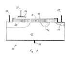
- the semiconductor component according to the invention shown in FIG. 1 is involved it is a transistor 10, which is manufactured in thin film SOI technology.
- An insulator layer 14 lies on a substrate 12, on which in turn a silicon film 16 is applied.
- the insulator 14 is thus below the silicon film 16 buried.
- Metallic contacts are on the top of transistor 10 attached, namely the source contact 18, the gate contact 20 and the Drain contact 22.
- the source contact 18 is attached in such a way that he on the one hand with the silicon film 16 and on the other hand simultaneously with the surface of the substrate 12 is contacted.
- the drain contact is in the same way 22, on an edge of the silicon film opposite the source contact 18 16 is attached, simultaneously with the silicon film 16 and the Contacted substrate 12.
- the gate contact 20 On the silicon film 16 is near the source contact 18 the gate contact 20 arranged, being between the metal contact 20 and the surface of the silicon film 16 a polysilicon layer 24 located. Also located on the bottom of the substrate 12 is the insulator 14 and the silicon film 16, a rear drain contact 26. Deviating from the embodiment shown here, this drain contact 26 also at another location on the upper surface of the substrate 12 may be arranged.
- anode shield 28 is provided for the source contact 18 and the gate contact 20, a buried p-n junction. In the same way is below the Drain contact 22 a cathode shield 30 is provided. Between the anode shield 28 and the cathode shield 30 there is a floating field ring 32 as a buried edge structure.
- the entire arrangement of the transistor 10 shown in FIG. 1 thus corresponds to one well-known transistor in thin-film SOI technology, based on an edge structure 28,30,32.
- the source contact 18 and the gate contact 20 of the transistor 10 are immediately above the anode region 28 of the Edge structure and are thus shielded from interfering fields.
- the drain contact 22 lies on the cathode side 30 of the edge structure.
- the drain contact 22 does not have to necessarily be contacted with the substrate 12.
- Be contacted must be the shield area over which the majority of the reverse voltage drops. If the blocking p-n junction is sufficiently contacted and that fits SOI component to the horizontal voltage curve, is unnecessary below Under certain circumstances, further contacting of the SOI component. In this case can have high doping in silicon film 16 of the opposite doping type as a shield trough take on the properties of a channel stopper.
- the transistor arrangement 10 may only have positive drain-source voltages operated, the highest potential at the rear drain contact 26 must be. Are the doping chosen opposite, i.e. the Substrate 12 is p-doped and shield 28 is n-doped, so there are only negatives Drain-source voltages allowed.
- the stress relief takes place via the edge structure, the floating field ring 32 includes.
- the channel stopper 30 prevents the expansion of the space charge beyond the boundary of the structure and at the same time protects the drain contact 22 in front of disturbing fields. It is also possible instead of the floating field ring 32 either a VLE structure or a JTE structure as a buried edge structure to use.
- transistor 10 instead of the transistor 10 according to the invention shown, others can also be used Semiconductor components, such as diodes, voltage-resistant resistors, IGBTs and the like realize.
- the arrangement of the anode contact of the diode corresponds in this case to the arrangement of the source contact described above 18, while the cathode contact corresponds to the drain contact 22.
- the electrical behavior of the described transistor 10 as a discrete component can be described as follows: Is on the drain contacts 22,26 a high positive voltage is applied and source 18 and gate 20 are on Maintained, there is a build-up between source 18 and drain 22 Space charge region. This is compared to completely isolated SOI components Space charge zone not only built up in the silicon film 16, but by contacting the substrate 12 also below the silicon film 16. This leads to a much more homogeneous space charge zone profile than it does otherwise occurs in the relatively thin silicon film 16. A curvature of the space charge zone hardly occurs there.
- the field lines below the SOI layer 14, 16 run analogously to a conventional one Edge structure.
- the space charge zone is defined by the field rings 32 significantly influenced below the silicon film 16. The further the space charge zone expands in the substrate 12 in the lateral direction, the further it also expands in silicon film 16. This creates a more homogeneous breakdown the space charge zone in the silicon film 16.
- the doping in silicon film 16 is equal to or less than that of the drift region the static avalanche breakdown always occurs in the substrate 12, whereby an optimal blocking capability for the transistor 10 according to the invention is achieved.
- the locking capability of the entire system is then exclusive on the layer structure of the substrate 12 and the arrangement and depth of the field rings 32 or another selected border structure.
- FIG. 2 shows an enlarged representation of the area of a transistor 10, in which is the anode shield 28.
- the insulator 14 and the silicon layer 16 are stacked on top of one another in a known manner.
- the source contact is at the left edge of the insulator layer 14 in FIG. 2 18 attached in such a way that a field oxide layer 34 on the one hand on the edge of the buried insulator 14 and on the other hand on the anode shield 28 rests.
- the field oxide layer 34 is covered by an intermediate oxide layer 36 enclosed.
- the gate contact 20, on the other hand includes the one already in FIG Fig. 1 described poly-silicon layer 24, which is similar to the field oxide layer 34 is covered by an intermediate oxide layer 38.
- Fig. 3 shows the circuit diagram a bridge circuit 42, in which the transistor 10 as a level shift transistor is integrated.
- the bridge circuit 42 further comprises a control unit 44, which includes driver, monitoring and sensor functions and in which Circuit diagram in Fig. 3 is only shown schematically.
- the control unit 44 is on the drain contact of transistor 10 connected while its source contact lies on ground.
- a so-called bypass 46 which is approximated by a Equivalent circuit diagram with a parallel connection of a diode 48 and a resistor 50 can be described.
- the control unit 44 is in turn connected to the gate contact of an IGBT 52 as a high-side switch, the drain contact of which is at the intermediate voltage U ZW and the source contact of which is in contact with the load. Also connected to the load are the opposite output of the bypass 50 and the drain contact of a further transistor 54 as a low-side switch, the source contact of which is connected to ground.
- the present invention enables the circuit unit in FIG. 3 to be monolithic to integrate on a chip. This results in enormous cost advantages and a space saving. At the same time, the system stability is increased, and the Effort in assembly and connection technology is reduced. Also revealed short signal transit times, which in turn enable short reaction times, for example when the switch is faulty.
- the switching information for the circuit breaker is transmitted to the control unit 44 by means of level control of the transistor 10.
- the control unit 44 switches the IGBT 52 on inversely to the high-voltage transistor.
- the IGBT 52 switches on, the entire intermediate circuit voltage U ZW being built up via the high-voltage transistor.
- the drift section of the IGBT 52 is enriched with charge carriers.
- This so-called charge carrier plasma is created by the electron current flowing in the IGBT channel and the hole current 56 caused by it, which is produced by injection at the rear pn junction. Since the hole current 56 is influenced neither by the channel nor by the blocking pn junction, but by the potential profile in the IGBT 52, a current flow, a so-called parasitic bypass current, also occurs in the p-well 58 and thus in the source 18 of the transistor 10. This manifests itself as an increased leakage current at the source contact of the transistor 10, but not at its drain contact 22.
- the full intermediate circuit voltage U ZW is present at the bypass diode 48, which connects the two electrodes.
- the total parasitic current at transistor 10 is thus composed of the SOI reverse current, the reverse current of the bypass diode 48 and the extracted hole current 56 coming from the rear.
- the transistor 10 In order to keep this current as small as possible, the transistor 10 should be spatially as far as possible from the active area of IGBT 52. This will the resistance to be overcome, the SOI bypass resistance, for the hole current 56 increased. Also the coupling of the hole current 56 to the electrode current leads to a lower bypass hole flow.
- IGBT 52 If the IGBT 52 is replaced by a power MOS transistor, can no hole current is generated due to the lack of rear side injection. So that is a parasitic bypass current is excluded.
- the blocking case is described in connection with FIG. 5.
- the drain contact and the source contact of the IGBT 52 and the drain contact of the transistor 10 according to the invention are here at a high positive potential corresponding to the intermediate circuit voltage U ZW . This means that the reverse voltage reduction takes place laterally and vertically only in transistor 10. This state represents the most critical load case for the high-voltage transistor.
- the space charge zone is formed only in the silicon film 16 and in the substrate 12 in the region of the transistor 10.
- FIG. 6 shows the blocking case in which the drain contact of the IGBT 52 is at a high potential corresponding to the intermediate circuit voltage U ZW , while the other electrodes are approximately at ground.
- the space charge zone 60 is broken down vertically in the entire chip in all areas. Only on the outer edge structure 62 does the space charge zone 60 also degrade in the lateral direction. In the bridge circuit shown in Fig. 3, this case applies to the upper switch when the lower switch is on. The intermediate circuit voltage U ZW is picked up by the upper switch.
Landscapes
- Thin Film Transistor (AREA)
- Bipolar Transistors (AREA)
Abstract
Description
- Fig. 1
- zeigt einen schematischen Schnitt durch ein erfindungsgemäßes laterales Halbleiterbauelement;
- Fig. 2
- zeigt einen Teilschnitt des Anodenbereichs eines erfindungsgemäßen Halbleiterbauelements gemäß Fig. 1;
- Fig. 3
- ist ein Schaltbild einer Schaltung mit einem erfindungsgemäßen Halbleiterbauelement als Transistor;
- Fig. 4
- ist eine schematische Darstellung eines Brückenschalters aus der Schaltung in Fig. 3;
- Fig. 5
- ist eine Darstellung des Brückenschalters entsprechend Fig. 4 in einem anderen Schaltungszustand; und
- Fig. 6
- zeigt den Brückenschalter aus den Figuren 4 und 5 im Sperrzustand.
Claims (15)
- Laterales Halbleiterbauelement (10) in Dünnfilm-SOI-Technik, mit einer Isolatorschicht (14), die auf einem Substrat (12) aufliegt und unter einem dünnen Siliziumfilm (16) vergraben ist, auf welchem der Source- bzw. Anoden-Kontakt (18) und der Drain- bzw. Kathoden-Kontakt (22) angebracht sind, dadurch gekennzeichnet, dass der Anoden-Kontakt (18) und der Kathoden-Kontakt (22) jeweils über getrennten Shield-Gebieten (28,30) innerhalb des Substrats (12) liegen, wobei der Anoden-Kontakt (18) mit dem Substrat (12) elektrisch verbunden ist.
- Laterales Halbleiterbauelement gemäß Anspruch 1, dadurch gekennzeichnet, dass die Shield-Gebiete (28,30) des Anoden- und des Kathoden-Kontaktes (18,22) durch eine dazwischen angeordnete vergrabene Randstruktur (32) voneinander isoliert sind.
- Laterales Halbleiterbauelement gemäß Anspruch 2, dadurch gekennzeichnet, dass die vergrabene Randstruktur (32) durch eine floatende Feldringstruktur gebildet wird.
- Laterales Halbleiterbauelement gemäß Anspruch 2, dadurch gekennzeichnet, dass die vergrabene Randstruktur (32) durch eine VLD-Struktur gebildet wird.
- Laterales Halbleiterbauelement gemäß Anspruch 2, dadurch gekennzeichnet, dass die vergrabene Randstruktur (32) durch eine JTE-Struktur gebildet wird.
- Laterales Halbleiterbauelement gemäß einem der Ansprüche 1 bis 5, dadurch gekennzeichnet, dass die elektrische Verbindung des Anoden-Kontaktes (18) mit dem Substrat (12) durch einen metallischen Kontakt hergestellt ist.
- Laterales Halbleiterbauelement gemäß einem der Ansprüche 1 bis 5, dadurch gekennzeichnet, dass die elektrische Verbindung des Anoden-Kontaktes (18) mit dem Substrat (12) durch ein elektrisches Bauelement hergestellt ist.
- Laterales Halbleiterbauelement gemäß einem der vorhergehenden Ansprüche, dadurch gekennzeichnet, dass der Kathoden-Kontakt (22) mit dem Substrat (12) elektrisch verbunden ist.
- Laterales Halbleiterbauelement gemäß einem der vorhergehenden Ansprüche, dadurch gekennzeichnet, dass das Halbleiterbauelement (10) einen Transistor darstellt.
- Laterales Halbleiterbauelement gemäß einem der Ansprüche 1 bis 8, dadurch gekennzeichnet, dass das Halbleiterbauelement (10) eine Diode darstellt.
- Laterales Halbleiterbauelement gemäß einem der Ansprüche 1 bis 8, dadurch gekennzeichnet, dass das Halbleiterbauelement (10) einen spannungsfesten Widerstand darstellt.
- Laterales Halbleiterbauelement gemäß einem der Ansprüche 1 bis 8, dadurch gekennzeichnet, dass das Halbleiterbauelement (10) einen IGBT darstellt.
- Halbleiterschaltung mit einem Halbleiterbauelement gemäß Anspruch 9, dadurch gekennzeichnet, dass das Halbleiterbauelement (10) ein Level-Shift-Transistor ist und in eine Treiberschaltung (42) mit einem vertikalen Leistungsbauelement wie etwa einem IGBT, einem DMOS oder dergleichen integriert ist.
- Halbleiterschaltung mit einem Halbleiterbauelement gemäß Anspruch 10, dadurch gekennzeichnet, dass das Halbleiterbauelement (10) eine SOI-Diode ist und als Entkopplungsdiode in eine Auswerteschaltung mit einem vertikalen Leistungsbauelement wie etwa einem IGBT, einem DMOS oder dergleichen integriert ist.
- Halbleiterschaltung mit Halbleiterbauelementen gemäß den Ansprüchen 6 und 7, dadurch gekennzeichnet, dass eine Anzahl von Transistoren und Dioden zu einer Brückentreiberschaltung geschaltet sind.
Applications Claiming Priority (2)
| Application Number | Priority Date | Filing Date | Title |
|---|---|---|---|
| DE10106359A DE10106359C1 (de) | 2001-02-12 | 2001-02-12 | Laterales Halbleiterbauelement in Dünnfilm-SOI-Technik |
| DE10106359 | 2001-02-12 |
Publications (3)
| Publication Number | Publication Date |
|---|---|
| EP1231645A2 true EP1231645A2 (de) | 2002-08-14 |
| EP1231645A3 EP1231645A3 (de) | 2004-12-08 |
| EP1231645B1 EP1231645B1 (de) | 2006-08-30 |
Family
ID=7673695
Family Applications (1)
| Application Number | Title | Priority Date | Filing Date |
|---|---|---|---|
| EP01129043A Expired - Lifetime EP1231645B1 (de) | 2001-02-12 | 2001-12-07 | Laterales Halbleiterbauelement in Dünnfilm-SOI-Technik |
Country Status (4)
| Country | Link |
|---|---|
| US (1) | US6693327B2 (de) |
| EP (1) | EP1231645B1 (de) |
| JP (1) | JP2002305207A (de) |
| DE (2) | DE10106359C1 (de) |
Cited By (1)
| Publication number | Priority date | Publication date | Assignee | Title |
|---|---|---|---|---|
| CN102361031A (zh) * | 2011-10-19 | 2012-02-22 | 电子科技大学 | 一种用于soi高压集成电路的半导体器件 |
Families Citing this family (67)
| Publication number | Priority date | Publication date | Assignee | Title |
|---|---|---|---|---|
| JP4431055B2 (ja) | 2003-01-13 | 2010-03-10 | コンティネンタル・テーベス・アクチエンゲゼルシヤフト・ウント・コンパニー・オッフェネ・ハンデルスゲゼルシヤフト | 集積部品 |
| US20060276043A1 (en) * | 2003-03-21 | 2006-12-07 | Johnson Mark A L | Method and systems for single- or multi-period edge definition lithography |
| EP1623495B1 (de) | 2003-05-06 | 2009-10-07 | Enecsys Limited | Stromversorgungsschaltungen |
| US8067855B2 (en) * | 2003-05-06 | 2011-11-29 | Enecsys Limited | Power supply circuits |
| DE102004006002B3 (de) * | 2004-02-06 | 2005-10-06 | eupec Europäische Gesellschaft für Leistungshalbleiter mbH | Soi-Halbleiterbauelement mit erhöhter Spannungsfestigkeit |
| WO2006048689A2 (en) * | 2004-11-08 | 2006-05-11 | Encesys Limited | Integrated circuits and power supplies |
| JP4944460B2 (ja) * | 2005-03-30 | 2012-05-30 | オンセミコンダクター・トレーディング・リミテッド | 半導体装置 |
| DE102005044165A1 (de) * | 2005-09-15 | 2007-03-29 | Infineon Technologies Ag | Halbleiterbauelement mit einem pn-Übergang und Verfahren zum Herstellen desselben |
| DE102005045910B4 (de) * | 2005-09-26 | 2010-11-11 | Infineon Technologies Austria Ag | Laterales SOI-Bauelement mit einem verringerten Einschaltwiderstand |
| US11881814B2 (en) | 2005-12-05 | 2024-01-23 | Solaredge Technologies Ltd. | Testing of a photovoltaic panel |
| US10693415B2 (en) | 2007-12-05 | 2020-06-23 | Solaredge Technologies Ltd. | Testing of a photovoltaic panel |
| JP2008085186A (ja) * | 2006-09-28 | 2008-04-10 | Sanyo Electric Co Ltd | 半導体装置 |
| JP2008085187A (ja) * | 2006-09-28 | 2008-04-10 | Sanyo Electric Co Ltd | 半導体装置 |
| US9130401B2 (en) | 2006-12-06 | 2015-09-08 | Solaredge Technologies Ltd. | Distributed power harvesting systems using DC power sources |
| US8319483B2 (en) | 2007-08-06 | 2012-11-27 | Solaredge Technologies Ltd. | Digital average input current control in power converter |
| US11888387B2 (en) | 2006-12-06 | 2024-01-30 | Solaredge Technologies Ltd. | Safety mechanisms, wake up and shutdown methods in distributed power installations |
| US8319471B2 (en) | 2006-12-06 | 2012-11-27 | Solaredge, Ltd. | Battery power delivery module |
| US9112379B2 (en) | 2006-12-06 | 2015-08-18 | Solaredge Technologies Ltd. | Pairing of components in a direct current distributed power generation system |
| US8384243B2 (en) | 2007-12-04 | 2013-02-26 | Solaredge Technologies Ltd. | Distributed power harvesting systems using DC power sources |
| US12316274B2 (en) | 2006-12-06 | 2025-05-27 | Solaredge Technologies Ltd. | Pairing of components in a direct current distributed power generation system |
| US9088178B2 (en) | 2006-12-06 | 2015-07-21 | Solaredge Technologies Ltd | Distributed power harvesting systems using DC power sources |
| US11569659B2 (en) | 2006-12-06 | 2023-01-31 | Solaredge Technologies Ltd. | Distributed power harvesting systems using DC power sources |
| US11687112B2 (en) | 2006-12-06 | 2023-06-27 | Solaredge Technologies Ltd. | Distributed power harvesting systems using DC power sources |
| US11855231B2 (en) | 2006-12-06 | 2023-12-26 | Solaredge Technologies Ltd. | Distributed power harvesting systems using DC power sources |
| US11735910B2 (en) | 2006-12-06 | 2023-08-22 | Solaredge Technologies Ltd. | Distributed power system using direct current power sources |
| US8947194B2 (en) | 2009-05-26 | 2015-02-03 | Solaredge Technologies Ltd. | Theft detection and prevention in a power generation system |
| US11296650B2 (en) | 2006-12-06 | 2022-04-05 | Solaredge Technologies Ltd. | System and method for protection during inverter shutdown in distributed power installations |
| US8618692B2 (en) | 2007-12-04 | 2013-12-31 | Solaredge Technologies Ltd. | Distributed power system using direct current power sources |
| US8473250B2 (en) | 2006-12-06 | 2013-06-25 | Solaredge, Ltd. | Monitoring of distributed power harvesting systems using DC power sources |
| US8816535B2 (en) | 2007-10-10 | 2014-08-26 | Solaredge Technologies, Ltd. | System and method for protection during inverter shutdown in distributed power installations |
| US11309832B2 (en) | 2006-12-06 | 2022-04-19 | Solaredge Technologies Ltd. | Distributed power harvesting systems using DC power sources |
| US8963369B2 (en) | 2007-12-04 | 2015-02-24 | Solaredge Technologies Ltd. | Distributed power harvesting systems using DC power sources |
| US8013472B2 (en) | 2006-12-06 | 2011-09-06 | Solaredge, Ltd. | Method for distributed power harvesting using DC power sources |
| US7791139B2 (en) | 2007-07-27 | 2010-09-07 | Infineon Technologies Austria Ag | Integrated circuit including a semiconductor assembly in thin-SOI technology |
| US8049523B2 (en) | 2007-12-05 | 2011-11-01 | Solaredge Technologies Ltd. | Current sensing on a MOSFET |
| US11264947B2 (en) | 2007-12-05 | 2022-03-01 | Solaredge Technologies Ltd. | Testing of a photovoltaic panel |
| EP2232690B1 (de) | 2007-12-05 | 2016-08-31 | Solaredge Technologies Ltd. | Parallel geschaltete umrichter |
| EP3496258B1 (de) | 2007-12-05 | 2025-02-05 | Solaredge Technologies Ltd. | Sicherheitsmechanismus in verteilten strominstallationen |
| WO2009072075A2 (en) | 2007-12-05 | 2009-06-11 | Solaredge Technologies Ltd. | Photovoltaic system power tracking method |
| EP4145691A1 (de) | 2008-03-24 | 2023-03-08 | Solaredge Technologies Ltd. | Schaltwandler mit einem hilfskommutierungsschaltkreis zur nullstromschaltung |
| EP3121922B1 (de) | 2008-05-05 | 2020-03-04 | Solaredge Technologies Ltd. | Gleichstromleistungskombinierer |
| US20100117153A1 (en) * | 2008-11-07 | 2010-05-13 | Honeywell International Inc. | High voltage soi cmos device and method of manufacture |
| US8106487B2 (en) | 2008-12-23 | 2012-01-31 | Pratt & Whitney Rocketdyne, Inc. | Semiconductor device having an inorganic coating layer applied over a junction termination extension |
| US12418177B2 (en) | 2009-10-24 | 2025-09-16 | Solaredge Technologies Ltd. | Distributed power system using direct current power sources |
| GB2485527B (en) | 2010-11-09 | 2012-12-19 | Solaredge Technologies Ltd | Arc detection and prevention in a power generation system |
| US10673229B2 (en) | 2010-11-09 | 2020-06-02 | Solaredge Technologies Ltd. | Arc detection and prevention in a power generation system |
| US10673222B2 (en) | 2010-11-09 | 2020-06-02 | Solaredge Technologies Ltd. | Arc detection and prevention in a power generation system |
| US10230310B2 (en) | 2016-04-05 | 2019-03-12 | Solaredge Technologies Ltd | Safety switch for photovoltaic systems |
| GB2486408A (en) | 2010-12-09 | 2012-06-20 | Solaredge Technologies Ltd | Disconnection of a string carrying direct current |
| GB2483317B (en) | 2011-01-12 | 2012-08-22 | Solaredge Technologies Ltd | Serially connected inverters |
| US8570005B2 (en) | 2011-09-12 | 2013-10-29 | Solaredge Technologies Ltd. | Direct current link circuit |
| GB2498365A (en) | 2012-01-11 | 2013-07-17 | Solaredge Technologies Ltd | Photovoltaic module |
| GB2498791A (en) | 2012-01-30 | 2013-07-31 | Solaredge Technologies Ltd | Photovoltaic panel circuitry |
| US9853565B2 (en) | 2012-01-30 | 2017-12-26 | Solaredge Technologies Ltd. | Maximized power in a photovoltaic distributed power system |
| GB2498790A (en) | 2012-01-30 | 2013-07-31 | Solaredge Technologies Ltd | Maximising power in a photovoltaic distributed power system |
| GB2499991A (en) | 2012-03-05 | 2013-09-11 | Solaredge Technologies Ltd | DC link circuit for photovoltaic array |
| US9087707B2 (en) | 2012-03-26 | 2015-07-21 | Infineon Technologies Austria Ag | Semiconductor arrangement with a power transistor and a high voltage device integrated in a common semiconductor body |
| US10115841B2 (en) | 2012-06-04 | 2018-10-30 | Solaredge Technologies Ltd. | Integrated photovoltaic panel circuitry |
| US9941813B2 (en) | 2013-03-14 | 2018-04-10 | Solaredge Technologies Ltd. | High frequency multi-level inverter |
| US9548619B2 (en) | 2013-03-14 | 2017-01-17 | Solaredge Technologies Ltd. | Method and apparatus for storing and depleting energy |
| EP2779251B1 (de) | 2013-03-15 | 2019-02-27 | Solaredge Technologies Ltd. | Umgehungsmechanismus |
| US9318974B2 (en) | 2014-03-26 | 2016-04-19 | Solaredge Technologies Ltd. | Multi-level inverter with flying capacitor topology |
| US11177663B2 (en) | 2016-04-05 | 2021-11-16 | Solaredge Technologies Ltd. | Chain of power devices |
| US12057807B2 (en) | 2016-04-05 | 2024-08-06 | Solaredge Technologies Ltd. | Chain of power devices |
| US11018623B2 (en) | 2016-04-05 | 2021-05-25 | Solaredge Technologies Ltd. | Safety switch for photovoltaic systems |
| US10074685B1 (en) | 2017-05-17 | 2018-09-11 | Prismatic Sensors Ab | X-ray sensor, x-ray detector system and x-ray imaging system |
| DE102024135471B3 (de) | 2024-09-26 | 2026-02-05 | Infineon Technologies Austria Ag | Halbleiter-auf-isolator-vorrichtung mit einem basissubstrat mit feldkontrollbereich |
Family Cites Families (5)
| Publication number | Priority date | Publication date | Assignee | Title |
|---|---|---|---|---|
| JPS625662A (ja) * | 1985-07-01 | 1987-01-12 | Nec Corp | Soi型高耐圧ic |
| JPH0832040A (ja) * | 1994-07-14 | 1996-02-02 | Nec Corp | 半導体装置 |
| JPH08153880A (ja) * | 1994-09-29 | 1996-06-11 | Toshiba Corp | 半導体装置及びその製造方法 |
| DE4441724A1 (de) * | 1994-11-23 | 1996-05-30 | Siemens Ag | SOI-Substrat |
| US5677562A (en) * | 1996-05-14 | 1997-10-14 | General Instrument Corporation Of Delaware | Planar P-N junction semiconductor structure with multilayer passivation |
-
2001
- 2001-02-12 DE DE10106359A patent/DE10106359C1/de not_active Expired - Fee Related
- 2001-12-07 EP EP01129043A patent/EP1231645B1/de not_active Expired - Lifetime
- 2001-12-07 DE DE50110873T patent/DE50110873D1/de not_active Expired - Lifetime
-
2002
- 2002-02-08 JP JP2002032253A patent/JP2002305207A/ja active Pending
- 2002-02-12 US US10/074,605 patent/US6693327B2/en not_active Expired - Lifetime
Cited By (1)
| Publication number | Priority date | Publication date | Assignee | Title |
|---|---|---|---|---|
| CN102361031A (zh) * | 2011-10-19 | 2012-02-22 | 电子科技大学 | 一种用于soi高压集成电路的半导体器件 |
Also Published As
| Publication number | Publication date |
|---|---|
| US20020121664A1 (en) | 2002-09-05 |
| DE10106359C1 (de) | 2002-09-05 |
| EP1231645B1 (de) | 2006-08-30 |
| US6693327B2 (en) | 2004-02-17 |
| JP2002305207A (ja) | 2002-10-18 |
| DE50110873D1 (de) | 2006-10-12 |
| EP1231645A3 (de) | 2004-12-08 |
Similar Documents
| Publication | Publication Date | Title |
|---|---|---|
| EP1231645B1 (de) | Laterales Halbleiterbauelement in Dünnfilm-SOI-Technik | |
| EP0566639B1 (de) | Integrierte leistungsschalterstruktur | |
| DE60319899T2 (de) | Doppeldiffundierter MOSFET | |
| DE102004014744B4 (de) | Halbleiterbaugruppe mit einem Graben zum Treiben eines Schaltselement und Vermeiden eines Latch-up Durchbruchs | |
| DE69416950T2 (de) | DMOSFET mit einem Widerstand zum Verbessern der Stromführung im Sperrbetrieb | |
| DE69316256T2 (de) | Hochspannungstruktur mit oxydisolierter Source und RESURF-Drift-Zone in Massivsilizium | |
| DE19630740B4 (de) | Bipolarer Transistor mit Kurzschlußanode und seitlich angeordneter isolierter Gate-Elektrode | |
| DE112016006255T5 (de) | Halbleitervorrichtung | |
| EP0905780A2 (de) | Integrierte Halbleiterschaltung mit Schutzstruktur zum Schutz vor elektrostatischer Entladung | |
| EP0905782B1 (de) | Integrierte Halbleiterschaltung mit Schutzstruktur zum Schutz vor elektrostatischer Entladung | |
| EP1320133A2 (de) | IGBT mit Trench-Gate-Struktur | |
| DE19918028A1 (de) | Halbleiter-Bauelement | |
| DE102008050495A1 (de) | Halbleitervorrichtung | |
| DE19814675A1 (de) | Ausgabeschaltung für einen Leistungs-IC mit hoher Durchbruchsspannung | |
| DE102009038776B9 (de) | Halbleitervorrichtung mit einem internen Isoliertgatebipolartransistor | |
| DE19810338B4 (de) | Bipolartransistor mir isoliertem Gate | |
| DE19534388B4 (de) | IGBT-Transistorbauteil | |
| DE69421758T2 (de) | Halbleiteranordnung mit einem Schutzmittel | |
| WO1994006158A1 (de) | Feldeffektgesteurtes halbleiterbauelement | |
| EP1259989B1 (de) | Monolithisch integriertes halbleiterbauelement | |
| DE102010020884B4 (de) | Halbleiterbauelement | |
| DE69834451T2 (de) | Schutzvorrichtung für einen integrierten MOS-Transistor gengen Spannungsgradienten | |
| DE102023120017A1 (de) | Halbleitervorrichtung | |
| DE69516952T2 (de) | Thyristor mit isoliertem Gate | |
| DE102015116099B3 (de) | Integrierte schaltung mit einer vielzahl von transistoren und zumindest einer spannungsbegrenzenden struktur |
Legal Events
| Date | Code | Title | Description |
|---|---|---|---|
| PUAI | Public reference made under article 153(3) epc to a published international application that has entered the european phase |
Free format text: ORIGINAL CODE: 0009012 |
|
| AK | Designated contracting states |
Kind code of ref document: A2 Designated state(s): AT BE CH CY DE DK ES FI FR GB GR IE IT LI LU MC NL PT SE TR |
|
| AX | Request for extension of the european patent |
Free format text: AL;LT;LV;MK;RO;SI |
|
| RAP1 | Party data changed (applicant data changed or rights of an application transferred) |
Owner name: EUPECEUROPAEISCHE GESELLSCHAFT FUERLEISTUNGSHALBLE |
|
| PUAL | Search report despatched |
Free format text: ORIGINAL CODE: 0009013 |
|
| AK | Designated contracting states |
Kind code of ref document: A3 Designated state(s): AT BE CH CY DE DK ES FI FR GB GR IE IT LI LU MC NL PT SE TR |
|
| AX | Request for extension of the european patent |
Extension state: AL LT LV MK RO SI |
|
| RIC1 | Information provided on ipc code assigned before grant |
Ipc: 7H 01L 29/786 A Ipc: 7H 01L 27/12 B |
|
| 17P | Request for examination filed |
Effective date: 20050606 |
|
| AKX | Designation fees paid |
Designated state(s): DE FR GB |
|
| GRAP | Despatch of communication of intention to grant a patent |
Free format text: ORIGINAL CODE: EPIDOSNIGR1 |
|
| GRAS | Grant fee paid |
Free format text: ORIGINAL CODE: EPIDOSNIGR3 |
|
| GRAA | (expected) grant |
Free format text: ORIGINAL CODE: 0009210 |
|
| RAP1 | Party data changed (applicant data changed or rights of an application transferred) |
Owner name: INFINEON TECHNOLOGIES AG |
|
| AK | Designated contracting states |
Kind code of ref document: B1 Designated state(s): DE FR GB |
|
| REG | Reference to a national code |
Ref country code: GB Ref legal event code: FG4D Free format text: NOT ENGLISH |
|
| REF | Corresponds to: |
Ref document number: 50110873 Country of ref document: DE Date of ref document: 20061012 Kind code of ref document: P |
|
| ET | Fr: translation filed | ||
| PLBE | No opposition filed within time limit |
Free format text: ORIGINAL CODE: 0009261 |
|
| STAA | Information on the status of an ep patent application or granted ep patent |
Free format text: STATUS: NO OPPOSITION FILED WITHIN TIME LIMIT |
|
| 26N | No opposition filed |
Effective date: 20070531 |
|
| REG | Reference to a national code |
Ref country code: FR Ref legal event code: PLFP Year of fee payment: 15 |
|
| REG | Reference to a national code |
Ref country code: FR Ref legal event code: PLFP Year of fee payment: 16 |
|
| REG | Reference to a national code |
Ref country code: FR Ref legal event code: PLFP Year of fee payment: 17 |
|
| PGFP | Annual fee paid to national office [announced via postgrant information from national office to epo] |
Ref country code: DE Payment date: 20200224 Year of fee payment: 19 |
|
| PGFP | Annual fee paid to national office [announced via postgrant information from national office to epo] |
Ref country code: FR Payment date: 20201223 Year of fee payment: 20 Ref country code: GB Payment date: 20201223 Year of fee payment: 20 |
|
| REG | Reference to a national code |
Ref country code: DE Ref legal event code: R119 Ref document number: 50110873 Country of ref document: DE |
|
| PG25 | Lapsed in a contracting state [announced via postgrant information from national office to epo] |
Ref country code: DE Free format text: LAPSE BECAUSE OF NON-PAYMENT OF DUE FEES Effective date: 20210701 |
|
| REG | Reference to a national code |
Ref country code: GB Ref legal event code: PE20 Expiry date: 20211206 |
|
| PG25 | Lapsed in a contracting state [announced via postgrant information from national office to epo] |
Ref country code: GB Free format text: LAPSE BECAUSE OF EXPIRATION OF PROTECTION Effective date: 20211206 |