EP1221781A2 - Taktrückgewinnung - Google Patents
Taktrückgewinnung Download PDFInfo
- Publication number
- EP1221781A2 EP1221781A2 EP01440423A EP01440423A EP1221781A2 EP 1221781 A2 EP1221781 A2 EP 1221781A2 EP 01440423 A EP01440423 A EP 01440423A EP 01440423 A EP01440423 A EP 01440423A EP 1221781 A2 EP1221781 A2 EP 1221781A2
- Authority
- EP
- European Patent Office
- Prior art keywords
- signals
- clock
- bandpass
- path
- filter
- Prior art date
- Legal status (The legal status is an assumption and is not a legal conclusion. Google has not performed a legal analysis and makes no representation as to the accuracy of the status listed.)
- Granted
Links
- 238000011084 recovery Methods 0.000 title claims abstract description 5
- 230000005540 biological transmission Effects 0.000 claims abstract description 15
- 238000000034 method Methods 0.000 claims abstract description 12
- 230000003111 delayed effect Effects 0.000 claims abstract description 6
- 230000001419 dependent effect Effects 0.000 description 2
- 230000000694 effects Effects 0.000 description 1
- 239000000203 mixture Substances 0.000 description 1
- 230000010355 oscillation Effects 0.000 description 1
- 238000005070 sampling Methods 0.000 description 1
- 238000007493 shaping process Methods 0.000 description 1
- 230000003595 spectral effect Effects 0.000 description 1
- 230000002123 temporal effect Effects 0.000 description 1
- 230000036962 time dependent Effects 0.000 description 1
Images
Classifications
-
- H—ELECTRICITY
- H04—ELECTRIC COMMUNICATION TECHNIQUE
- H04L—TRANSMISSION OF DIGITAL INFORMATION, e.g. TELEGRAPHIC COMMUNICATION
- H04L25/00—Baseband systems
- H04L25/38—Synchronous or start-stop systems, e.g. for Baudot code
- H04L25/40—Transmitting circuits; Receiving circuits
- H04L25/49—Transmitting circuits; Receiving circuits using code conversion at the transmitter; using predistortion; using insertion of idle bits for obtaining a desired frequency spectrum; using three or more amplitude levels ; Baseband coding techniques specific to data transmission systems
-
- H—ELECTRICITY
- H04—ELECTRIC COMMUNICATION TECHNIQUE
- H04L—TRANSMISSION OF DIGITAL INFORMATION, e.g. TELEGRAPHIC COMMUNICATION
- H04L25/00—Baseband systems
- H04L25/02—Details ; arrangements for supplying electrical power along data transmission lines
- H04L25/20—Repeater circuits; Relay circuits
- H04L25/24—Relay circuits using discharge tubes or semiconductor devices
- H04L25/242—Relay circuits using discharge tubes or semiconductor devices with retiming
-
- H—ELECTRICITY
- H04—ELECTRIC COMMUNICATION TECHNIQUE
- H04L—TRANSMISSION OF DIGITAL INFORMATION, e.g. TELEGRAPHIC COMMUNICATION
- H04L7/00—Arrangements for synchronising receiver with transmitter
- H04L7/02—Speed or phase control by the received code signals, the signals containing no special synchronisation information
- H04L7/027—Speed or phase control by the received code signals, the signals containing no special synchronisation information extracting the synchronising or clock signal from the received signal spectrum, e.g. by using a resonant or bandpass circuit
Definitions
- the invention relates to a method for digital message transmission, at which the transmitted signals at the end of a transmission path by means of a Device for clock recovery sampled and then processed further and where the signals to a decision maker at the same time over two separate paths, a delay path and a path equipped with a filter (DE book “Digital and Analog Message Transmission” by Erich Pehl, Verlag Wegig, Heidelberg, 1998, pages 182, 183).
- the Receiver clock - the local clock - in frequency and phase on the clock of the incoming signals can be adjusted. This is necessary because of variation the transmission function of the transmission channel not only the shape of the received Signals (impulses) changes, but because the temporal position of each Pulse maximum shifts.
- the entire pulse shaping is also done by Temperature drift and tolerances of the components used in the transmitter and receiver or of the cable used as a transmission medium. It is therefore time-dependent and subject to a certain spread.
- the ratio of the useful signal to the interference signal (Signal-to-noise ratio) and thus the achievable bit error rate depends essentially on the described influencing factors. In all cases it must be ensured that the Sampling of the signals arriving at the receiver is still a further processing Size is obtained that does not exceed a predetermined limit Bit error rate guaranteed.
- the clock can for example from a continuous data signal by using a narrow-band filter can be recovered.
- a phase-controlled oscillator PLL circuit
- PLL circuit phase-controlled oscillator
- burst operation packet-switched Networks (burst operation) in which the data are compressed into bursts lie between the bursts data-free pauses and the bursts can be from different transmitters come. You can therefore have completely different phase positions.
- the methods mentioned are for clock recovery in networks with burst operation slow and therefore not suitable.
- the invention is based on the object, the method described above to further develop that it is also in a digital message transmission with burst operation can be used.
- the incoming signal is split into two separate paths as before split.
- a path lies the broadband bandpass, which is the clock oscillation filtered out the signal mixture.
- the filtered clock signal is then by the limiting amplifier processed.
- the settling time of the band pass is on Burst start less than its decay time or hold time after the end of the burst.
- the signals are delayed by a constant time that is less than however, the settling time of the bandpass is greater than its settling time.
- a clock-synchronous is used as the broadband bandpass Bandpass used.
- the signal to be filtered is on the one hand in two analog multipliers with the local clock and on the other hand with the local clock shifted by 90 ° multiplied.
- the real and imaginary parts of the complex are at the output of the multipliers Envelope of the signal available as two low-frequency signals.
- the two Envelope signals are band limited by two identical low-pass filters. On theirs Outputs, the now band-limited envelope is again with the local clock or multiplied the local clock shifted by 90 ° and to an output signal added.
- a signal current S consisting of bursts.
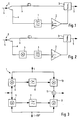
- the signal current S is on at input E. a path a and a delay path b characterized by two loops divided up.
- Path a contains a broadband bandpass filter 1 and a limiting amplifier 2 arranged.
- the delay path b and the output of the amplifier 2 are included connected to a decision maker 3, at the output of which the regenerated signal current S for Available.
- the bandwidth of the bandpass 1 is dependent on the bit clock of the one to be received Signal current selected.
- One measure of this is the filter quality Q, which is between 300 and 400 should lie. This corresponds to a relative bandwidth of approximately 0.3% of the bit clock. she for a signal stream with a bit clock of 10 Gbit / s is approximately 30 MHz. In this sense, the bandwidth of the bandpass filter 1 is selected so that it is between 0.2% and 0.4% of the bit clock of the signal stream to be received.
- bandpass 1 As soon as a burst of the signal stream S is present at the bandpass 1, the same begins to work. It has a settling time TE at the beginning of the burst, after which a bandpass 1 usable clock signal is supplied.
- the signal carried on the delay path b (Burst) is delayed by a longer time TV than the settling time TE.
- bandpass 1 At the At the end of the burst, bandpass 1 has a decay time TA. After that, no more clock signal delivered.
- the bandpass only delivers when the next burst of the signal stream S arrives 1 - as described - another clock signal. Since the signal on the Delay path b is delayed by the time TV, the swing-out time TA des Bandpass 1 should be larger than the time TV.
- the limiting amplifier 2 In order to realize the specified times in the sense described - TE ⁇ TV ⁇ TA can and the effects of amplitude fluctuations in the voltage at To avoid output of the bandpass 1, the limiting amplifier 2 must be connected to the same connected.
- the amplifier 2 delivers the filtered bandpass 1 Processed clock signal. Its threshold value is so in a preferred embodiment chosen to limit the clock signal at less than 1 ⁇ 4 of the maximum amplitude at the exit of the bandpass 1.
- the settling time TE of the bandpass 1 becomes therefore set much shorter than its swing-out time TA.
- the amplifier 2 lifts on the other hand, the level of the clock signal to a usable for further processing Value.
- the clock signal is given by the amplifier 2 to the decision maker 3, on which because of the condition TE ⁇ TV ⁇ TA during the entire length of the burst in-phase clock signal is available.
- a converter 4 (FIG. 2) into path a switched on, by which the NRZ code is converted into an RZ code.
- the clock frequency of the signal stream is thereby a spectral component in the signal stream reproduced.
- a clock-synchronous bandpass is used as bandpass 1, as is shown, for example, in FIG. 3:
- the signal to be filtered is multiplied in two analog multipliers 5 and 6 by the local clock t on the one hand and the local clock t shifted by 90 ° on the other.
- the real and imaginary parts of the complex envelope of the input signal are available as two low-frequency signals.
- These two signals are band-limited by two identical low-pass filters 7 and 8.
- the signals in analog multipliers 9 and 10 are again multiplied by the clock t or by the clock t shifted by 90 ° and added to the output signal in a summer 11, which is applied to the amplifier 2.
- This isochronous bandpass acts like a bandpass with the local clock t as Center frequency and a bandwidth equal to the cutting frequency of the two low passes 7 and 8. Although the output signal is generated from the local clock t, it is correct in Frequency and phase match the input signal if the difference between Input frequency and local clock frequency is within the set bandwidth.
- the multipliers 5 and 6 or 9 and 10 can by fast diode mixers be implemented.
- the cut-off frequency of the low-frequency signals also drops increasing quality Q and can be processed with fast operational amplifiers.
- sample & hold links Through the additional use of sample & hold links, the bandwidth of the Bandpass 1 can be changed according to FIG. 3. You can, if necessary Direction of transmission before the low passes 7 and 8 are arranged.
- Such sample & hold links can have a relatively wide range at the beginning of the burst for fast Start settling (short settling time TE) and then switch to low or zero bandwidth ensure a long decay time TA. It then turns out only a slight dependence of the clock signal on the signal content.
Landscapes
- Engineering & Computer Science (AREA)
- Computer Networks & Wireless Communication (AREA)
- Signal Processing (AREA)
- Power Engineering (AREA)
- Physics & Mathematics (AREA)
- Spectroscopy & Molecular Physics (AREA)
- Synchronisation In Digital Transmission Systems (AREA)
- Time-Division Multiplex Systems (AREA)
- Luminescent Compositions (AREA)
- Use Of Switch Circuits For Exchanges And Methods Of Control Of Multiplex Exchanges (AREA)
Abstract
Description
- daß als Filter ein breitbandiger Bandpaß mit einer relativen Bandbreite von 0,2 % bis 0,4 % des Bittaktes der übertragenen Signale eingesetzt wird, dessen Einschwingzeit kleiner als die Zeit ist, um welche die Signale auf dem Verzögerungspfad verzögert werden, die ihrerseits kleiner als die Ausschwingzeit des Bandpasses ist, und
- daß dem Bandpaß ein die Amplitude der Ausgangsspannung desselben begrenzender Verstärker nachgeschaltet wird, durch welchen die Taktsignale auf den erforderlichen, konstanten Pegel gebracht werden.
- N
- die maximal zu erwartende Länge einer 0 oder 1 Folge
- Umax
- der Maximalpegel am Ausgang des Bandpasses 1 bei Anliegen einer 0101 Folge
- Ulimit
- die Begrenzungsspannung für Vollaussteuerung des Verstärkers 2.
Das zu filternde Signal wird in zwei analogen Multiplizierern 5 und 6 mit dem lokalen Takt t einerseits sowie dem um 90° verschobenen lokalen Takt t andererseits multipliziert. Am Ausgang der Multiplizierer 5 und 6 stehen Real- und Imaginärteil der komplexen Einhüllenden des Eingangssignals als zwei niederfrequente Signale zur Verfügung. Diese beiden Signale werden durch zwei identische Tiefpässe 7 und 8 bandbegrenzt. An deren Ausgängen werden die Signale in analogen Multiplizierern 9 und 10 erneut mit dem Takt t bzw. mit dem um 90° verschobenen Takt t multipliziert und in einem Summierer 11 zum Ausgangssignal addiert, das dem Verstärker 2 aufgegeben wird.
Claims (5)
- Verfahren zur digitalen Nachrichtenübertragung, bei welchem die übertragenen Signale am Ende einer Übertragungsstrecke mittels einer Einrichtung zur Taktrückgewinnung abgetastet und anschließend weiterverarbeitet werden und bei welchem die Signale einem Entscheider gleichzeitig über zwei getrennte Pfade, einen Verzögerungspfad und einen mit einem Filter ausgerüsteten Pfad, zugeführt werden,
dadurch gekennzeichnet,daß als Filter ein breitbandiger Bandpaß (1) mit einer relativen Bandbreite von 0,2 % bis 0,4 % des Bittaktes der übertragenen Signale eingesetzt wird, dessen Einschwingzeit (TE) kleiner als die Zeit (TV) ist, um welche die Signale auf dem Verzögerungspfad (b) verzögert werden, die ihrerseits kleiner als die Ausschwingzeit (TA) des Bandpasses (1) ist, unddaß dem Bandpaß (1) ein die Amplitude der Ausgangsspannung desselben begrenzender Verstärker (2) nachgeschaltet wird, durch welchen die Taktsignale auf den erforderlichen, konstanten Pegel gebracht werden. - Verfahren nach Anspruch 1, dadurch gekennzeichnet, daß ein Bandpaß (1) mit einer relativen Bandbreite von 0,3 % des Bittaktes der übertragenen Signale verwendet wird.
- Verfahren nach Anspruch 1 oder 2, dadurch gekennzeichnet,daß als Bandpaß (1) eine Schaltung mit zwei parallelen Pfaden verwendet wird, in denen jeweils ein identischer Tiefpaß (7,8) zwischen zwei analogen Multiplizierern (5,9;6,10) angeordnet ist, unddaß die Multiplizierer (6,10) des einen Pfades mit dem lokalen Takt (t) beaufschlagt werden, während die Multiplizierer (5,9) des anderen Pfades mit dem um 90° verschobenen lokalen Takt (t) beaufschlagt werden.
- Verfahren nach Anspruch 3, dadurch gekennzeichnet, daß in Übertragungsrichtung vor den Tiefpässen (7,8) jeweils ein sample & hold-Glied eingeschaltet wird.
- Verfahren nach einem der Ansprüche 1 bis 4, dadurch gekennzeichnet, daß die Codierung der Signale vor dem Bandpaß (1) gegebenenfalls von einem NRZ-Code in einen RZ-Code umgewandelt wird.
Applications Claiming Priority (2)
| Application Number | Priority Date | Filing Date | Title |
|---|---|---|---|
| DE10100500A DE10100500A1 (de) | 2001-01-08 | 2001-01-08 | Verfahren zur digitalen Nachrichtenübertragung |
| DE10100500 | 2001-01-08 |
Publications (3)
| Publication Number | Publication Date |
|---|---|
| EP1221781A2 true EP1221781A2 (de) | 2002-07-10 |
| EP1221781A3 EP1221781A3 (de) | 2005-04-27 |
| EP1221781B1 EP1221781B1 (de) | 2007-04-11 |
Family
ID=7669945
Family Applications (1)
| Application Number | Title | Priority Date | Filing Date |
|---|---|---|---|
| EP01440423A Expired - Lifetime EP1221781B1 (de) | 2001-01-08 | 2001-12-19 | Taktrückgewinnung |
Country Status (4)
| Country | Link |
|---|---|
| US (1) | US20020101944A1 (de) |
| EP (1) | EP1221781B1 (de) |
| AT (1) | ATE359633T1 (de) |
| DE (2) | DE10100500A1 (de) |
Cited By (1)
| Publication number | Priority date | Publication date | Assignee | Title |
|---|---|---|---|---|
| US7340022B2 (en) | 2003-02-28 | 2008-03-04 | Alcatel | Method, a sender, a receiver, an optical network element and a serialized packet format for transmitting packets |
Families Citing this family (1)
| Publication number | Priority date | Publication date | Assignee | Title |
|---|---|---|---|---|
| US20040235423A1 (en) * | 2003-01-14 | 2004-11-25 | Interdigital Technology Corporation | Method and apparatus for network management using perceived signal to noise and interference indicator |
Family Cites Families (7)
| Publication number | Priority date | Publication date | Assignee | Title |
|---|---|---|---|---|
| FR2281008B1 (fr) * | 1974-07-30 | 1977-01-07 | Lignes Telegraph Telephon | Dispositif de regeneration de signaux d'horloge a partir d'impulsions ternaires |
| US4025720A (en) * | 1975-05-30 | 1977-05-24 | Gte Automatic Electric Laboratories Incorporated | Digital bit rate converter |
| JPS562761A (en) * | 1979-06-20 | 1981-01-13 | Nec Corp | Clock reproducing circuit |
| US4715049A (en) * | 1986-03-12 | 1987-12-22 | American Telephone And Telegraph Company, At&T Bell Laboratories | Clock recovery and retiming scheme with saw filter phase trimming to achieve desired system phase adjustment |
| US5276712A (en) * | 1989-11-16 | 1994-01-04 | Digital Equipment Corporation | Method and apparatus for clock recovery in digital communication systems |
| US5577056A (en) * | 1995-02-24 | 1996-11-19 | Hughes Aircraft Co. | Method and apparatus for adjusting the postamble false detection probability threshold for a burst transmission |
| US6075825A (en) * | 1998-01-06 | 2000-06-13 | Lucent Technologies, Inc. | Timing and data recovery circuit for ultra high speed optical communication system |
-
2001
- 2001-01-08 DE DE10100500A patent/DE10100500A1/de not_active Withdrawn
- 2001-12-19 EP EP01440423A patent/EP1221781B1/de not_active Expired - Lifetime
- 2001-12-19 DE DE50112326T patent/DE50112326D1/de not_active Expired - Fee Related
- 2001-12-19 AT AT01440423T patent/ATE359633T1/de not_active IP Right Cessation
-
2002
- 2002-01-07 US US10/036,391 patent/US20020101944A1/en not_active Abandoned
Cited By (1)
| Publication number | Priority date | Publication date | Assignee | Title |
|---|---|---|---|---|
| US7340022B2 (en) | 2003-02-28 | 2008-03-04 | Alcatel | Method, a sender, a receiver, an optical network element and a serialized packet format for transmitting packets |
Also Published As
| Publication number | Publication date |
|---|---|
| EP1221781B1 (de) | 2007-04-11 |
| EP1221781A3 (de) | 2005-04-27 |
| US20020101944A1 (en) | 2002-08-01 |
| DE50112326D1 (de) | 2007-05-24 |
| ATE359633T1 (de) | 2007-05-15 |
| DE10100500A1 (de) | 2002-07-11 |
Similar Documents
| Publication | Publication Date | Title |
|---|---|---|
| DE2902680C2 (de) | Bandpaßfilterschaltung | |
| DE2640325C3 (de) | Datenempfangsschaltung | |
| DE69406151T2 (de) | Einrichtung zur Synchronisierung eines lokalen Trägers, in OFDM-Systemen | |
| DE2629404A1 (de) | Automatische geraeuschsperre zur verarbeitung von demodulierten fm-signalen | |
| DE2928446C2 (de) | Schaltungsanordnung zur Synchronisation des Empfängers bei einer trägermodulierten Datenübertragung | |
| DE2735642C2 (de) | Phasenverriegelungsschleife | |
| DE2530467C3 (de) | Bandpaßfilter-Schaltung | |
| DE2027544C3 (de) | ||
| DE2656975C3 (de) | Verfahren zur Übertragung von modulierten Datensignalen mittels adaptiver Deltamodulation | |
| DE69232966T2 (de) | Taktwiedergewinnungsverfahren und -system | |
| DE2212917A1 (de) | Hochgeschwindigkeits-UEbertragungsempfaenger mit feiner Zeitsteuerung und Traegerphasenwiedergewinnung | |
| DE2720401C3 (de) | Datenempfänger mit einem Synchronisierfolge-Detektionskreis | |
| DE60116968T2 (de) | Daten-Slicer-Schaltung und RF-Empfänger, der diese Schaltung verwendet | |
| DE4316776A1 (de) | Frequenzmodulationsempfänger | |
| LU82155A1 (de) | System zum empfang frequenzmodulierter digitaler nachrichtensignale | |
| EP1221781A2 (de) | Taktrückgewinnung | |
| DE2813338C2 (de) | "Anordnung zum interpolierenden Umcodieren eines Deltamodulationssignals" | |
| DE2906886C2 (de) | Schaltungsanordnung zur Schrittakt-Gewinnung | |
| DE2946701C2 (de) | Schaltungsanordnung zur Regeneration von blockweise übertragenen Datenbits | |
| DE2738648C3 (de) | Schaltung zur Regeneration für insbesondere digitale Signale | |
| DE3015218C2 (de) | ||
| DE2500654C2 (de) | Schaltungsanordnung zur Pegelregelung eines Datensignals | |
| DE102017202879B4 (de) | Verfahren zur drathlosen seriellen Datenübertragung | |
| DE2632165B2 (de) | Schaltungsanordnung zum Regeln der Folgefrequenz von Taktimpulsen | |
| DE1297648B (de) | Verfahren und Schaltungsanordnung zur UEbertragung von binaer-kodierten Daten durch Anwendung von Frequenzmodulation |
Legal Events
| Date | Code | Title | Description |
|---|---|---|---|
| PUAI | Public reference made under article 153(3) epc to a published international application that has entered the european phase |
Free format text: ORIGINAL CODE: 0009012 |
|
| AK | Designated contracting states |
Kind code of ref document: A2 Designated state(s): AT BE CH CY DE DK ES FI FR GB GR IE IT LI LU MC NL PT SE TR |
|
| AX | Request for extension of the european patent |
Free format text: AL;LT;LV;MK;RO;SI |
|
| 17P | Request for examination filed |
Effective date: 20040804 |
|
| PUAL | Search report despatched |
Free format text: ORIGINAL CODE: 0009013 |
|
| AK | Designated contracting states |
Kind code of ref document: A3 Designated state(s): AT BE CH CY DE DK ES FI FR GB GR IE IT LI LU MC NL PT SE TR |
|
| AX | Request for extension of the european patent |
Extension state: AL LT LV MK RO SI |
|
| AKX | Designation fees paid |
Designated state(s): AT BE CH CY DE DK ES FI FR GB GR IE IT LI LU MC NL PT SE TR |
|
| GRAP | Despatch of communication of intention to grant a patent |
Free format text: ORIGINAL CODE: EPIDOSNIGR1 |
|
| GRAS | Grant fee paid |
Free format text: ORIGINAL CODE: EPIDOSNIGR3 |
|
| GRAA | (expected) grant |
Free format text: ORIGINAL CODE: 0009210 |
|
| RAP1 | Party data changed (applicant data changed or rights of an application transferred) |
Owner name: ALCATEL LUCENT |
|
| AK | Designated contracting states |
Kind code of ref document: B1 Designated state(s): AT BE CH CY DE DK ES FI FR GB GR IE IT LI LU MC NL PT SE TR |
|
| PG25 | Lapsed in a contracting state [announced via postgrant information from national office to epo] |
Ref country code: FI Free format text: LAPSE BECAUSE OF FAILURE TO SUBMIT A TRANSLATION OF THE DESCRIPTION OR TO PAY THE FEE WITHIN THE PRESCRIBED TIME-LIMIT Effective date: 20070411 |
|
| REG | Reference to a national code |
Ref country code: GB Ref legal event code: FG4D Free format text: NOT ENGLISH |
|
| REG | Reference to a national code |
Ref country code: CH Ref legal event code: EP |
|
| GBT | Gb: translation of ep patent filed (gb section 77(6)(a)/1977) |
Effective date: 20070425 |
|
| REG | Reference to a national code |
Ref country code: IE Ref legal event code: FG4D Free format text: LANGUAGE OF EP DOCUMENT: GERMAN |
|
| REF | Corresponds to: |
Ref document number: 50112326 Country of ref document: DE Date of ref document: 20070524 Kind code of ref document: P |
|
| PG25 | Lapsed in a contracting state [announced via postgrant information from national office to epo] |
Ref country code: SE Free format text: LAPSE BECAUSE OF FAILURE TO SUBMIT A TRANSLATION OF THE DESCRIPTION OR TO PAY THE FEE WITHIN THE PRESCRIBED TIME-LIMIT Effective date: 20070711 |
|
| PG25 | Lapsed in a contracting state [announced via postgrant information from national office to epo] |
Ref country code: ES Free format text: LAPSE BECAUSE OF FAILURE TO SUBMIT A TRANSLATION OF THE DESCRIPTION OR TO PAY THE FEE WITHIN THE PRESCRIBED TIME-LIMIT Effective date: 20070722 |
|
| PG25 | Lapsed in a contracting state [announced via postgrant information from national office to epo] |
Ref country code: PT Free format text: LAPSE BECAUSE OF FAILURE TO SUBMIT A TRANSLATION OF THE DESCRIPTION OR TO PAY THE FEE WITHIN THE PRESCRIBED TIME-LIMIT Effective date: 20070911 |
|
| ET | Fr: translation filed | ||
| NLV1 | Nl: lapsed or annulled due to failure to fulfill the requirements of art. 29p and 29m of the patents act | ||
| REG | Reference to a national code |
Ref country code: IE Ref legal event code: FD4D |
|
| PG25 | Lapsed in a contracting state [announced via postgrant information from national office to epo] |
Ref country code: DK Free format text: LAPSE BECAUSE OF FAILURE TO SUBMIT A TRANSLATION OF THE DESCRIPTION OR TO PAY THE FEE WITHIN THE PRESCRIBED TIME-LIMIT Effective date: 20070411 Ref country code: NL Free format text: LAPSE BECAUSE OF FAILURE TO SUBMIT A TRANSLATION OF THE DESCRIPTION OR TO PAY THE FEE WITHIN THE PRESCRIBED TIME-LIMIT Effective date: 20070411 Ref country code: IE Free format text: LAPSE BECAUSE OF FAILURE TO SUBMIT A TRANSLATION OF THE DESCRIPTION OR TO PAY THE FEE WITHIN THE PRESCRIBED TIME-LIMIT Effective date: 20070411 |
|
| PLBE | No opposition filed within time limit |
Free format text: ORIGINAL CODE: 0009261 |
|
| STAA | Information on the status of an ep patent application or granted ep patent |
Free format text: STATUS: NO OPPOSITION FILED WITHIN TIME LIMIT |
|
| 26N | No opposition filed |
Effective date: 20080114 |
|
| PG25 | Lapsed in a contracting state [announced via postgrant information from national office to epo] |
Ref country code: IT Free format text: LAPSE BECAUSE OF FAILURE TO SUBMIT A TRANSLATION OF THE DESCRIPTION OR TO PAY THE FEE WITHIN THE PRESCRIBED TIME-LIMIT Effective date: 20070411 Ref country code: GR Free format text: LAPSE BECAUSE OF FAILURE TO SUBMIT A TRANSLATION OF THE DESCRIPTION OR TO PAY THE FEE WITHIN THE PRESCRIBED TIME-LIMIT Effective date: 20070712 |
|
| PGFP | Annual fee paid to national office [announced via postgrant information from national office to epo] |
Ref country code: GB Payment date: 20071218 Year of fee payment: 7 |
|
| PGFP | Annual fee paid to national office [announced via postgrant information from national office to epo] |
Ref country code: DE Payment date: 20071221 Year of fee payment: 7 |
|
| BERE | Be: lapsed |
Owner name: ALCATEL LUCENT Effective date: 20071231 |
|
| PG25 | Lapsed in a contracting state [announced via postgrant information from national office to epo] |
Ref country code: MC Free format text: LAPSE BECAUSE OF NON-PAYMENT OF DUE FEES Effective date: 20071231 |
|
| PGFP | Annual fee paid to national office [announced via postgrant information from national office to epo] |
Ref country code: FR Payment date: 20071217 Year of fee payment: 7 |
|
| REG | Reference to a national code |
Ref country code: CH Ref legal event code: PL |
|
| PG25 | Lapsed in a contracting state [announced via postgrant information from national office to epo] |
Ref country code: BE Free format text: LAPSE BECAUSE OF NON-PAYMENT OF DUE FEES Effective date: 20071231 |
|
| PG25 | Lapsed in a contracting state [announced via postgrant information from national office to epo] |
Ref country code: LI Free format text: LAPSE BECAUSE OF NON-PAYMENT OF DUE FEES Effective date: 20071231 Ref country code: CH Free format text: LAPSE BECAUSE OF NON-PAYMENT OF DUE FEES Effective date: 20071231 |
|
| PG25 | Lapsed in a contracting state [announced via postgrant information from national office to epo] |
Ref country code: AT Free format text: LAPSE BECAUSE OF NON-PAYMENT OF DUE FEES Effective date: 20071219 |
|
| PG25 | Lapsed in a contracting state [announced via postgrant information from national office to epo] |
Ref country code: CY Free format text: LAPSE BECAUSE OF FAILURE TO SUBMIT A TRANSLATION OF THE DESCRIPTION OR TO PAY THE FEE WITHIN THE PRESCRIBED TIME-LIMIT Effective date: 20070411 |
|
| GBPC | Gb: european patent ceased through non-payment of renewal fee |
Effective date: 20081219 |
|
| PG25 | Lapsed in a contracting state [announced via postgrant information from national office to epo] |
Ref country code: LU Free format text: LAPSE BECAUSE OF NON-PAYMENT OF DUE FEES Effective date: 20071219 |
|
| PG25 | Lapsed in a contracting state [announced via postgrant information from national office to epo] |
Ref country code: TR Free format text: LAPSE BECAUSE OF FAILURE TO SUBMIT A TRANSLATION OF THE DESCRIPTION OR TO PAY THE FEE WITHIN THE PRESCRIBED TIME-LIMIT Effective date: 20070411 |
|
| REG | Reference to a national code |
Ref country code: FR Ref legal event code: ST Effective date: 20090831 |
|
| PG25 | Lapsed in a contracting state [announced via postgrant information from national office to epo] |
Ref country code: DE Free format text: LAPSE BECAUSE OF NON-PAYMENT OF DUE FEES Effective date: 20090701 |
|
| PG25 | Lapsed in a contracting state [announced via postgrant information from national office to epo] |
Ref country code: GB Free format text: LAPSE BECAUSE OF NON-PAYMENT OF DUE FEES Effective date: 20081219 |
|
| PG25 | Lapsed in a contracting state [announced via postgrant information from national office to epo] |
Ref country code: FR Free format text: LAPSE BECAUSE OF NON-PAYMENT OF DUE FEES Effective date: 20081231 |
|
| REG | Reference to a national code |
Ref country code: FR Ref legal event code: CA Effective date: 20150521 |
|
| REG | Reference to a national code |
Ref country code: FR Ref legal event code: CA Effective date: 20150521 |