EP1217659A2 - Leistungshalbleitermodul mit hoher Spannungsfestigkeit - Google Patents
Leistungshalbleitermodul mit hoher Spannungsfestigkeit Download PDFInfo
- Publication number
- EP1217659A2 EP1217659A2 EP01129819A EP01129819A EP1217659A2 EP 1217659 A2 EP1217659 A2 EP 1217659A2 EP 01129819 A EP01129819 A EP 01129819A EP 01129819 A EP01129819 A EP 01129819A EP 1217659 A2 EP1217659 A2 EP 1217659A2
- Authority
- EP
- European Patent Office
- Prior art keywords
- edge
- ceramic
- metallic
- power semiconductor
- lamination
- Prior art date
- Legal status (The legal status is an assumption and is not a legal conclusion. Google has not performed a legal analysis and makes no representation as to the accuracy of the status listed.)
- Granted
Links
Images


Classifications
-
- H—ELECTRICITY
- H05—ELECTRIC TECHNIQUES NOT OTHERWISE PROVIDED FOR
- H05K—PRINTED CIRCUITS; CASINGS OR CONSTRUCTIONAL DETAILS OF ELECTRIC APPARATUS; MANUFACTURE OF ASSEMBLAGES OF ELECTRICAL COMPONENTS
- H05K1/00—Printed circuits
- H05K1/02—Details
- H05K1/0213—Electrical arrangements not otherwise provided for
- H05K1/0254—High voltage adaptations; Electrical insulation details; Overvoltage or electrostatic discharge protection ; Arrangements for regulating voltages or for using plural voltages
- H05K1/0256—Electrical insulation details, e.g. around high voltage areas
-
- H—ELECTRICITY
- H10—SEMICONDUCTOR DEVICES; ELECTRIC SOLID-STATE DEVICES NOT OTHERWISE PROVIDED FOR
- H10W—GENERIC PACKAGES, INTERCONNECTIONS, CONNECTORS OR OTHER CONSTRUCTIONAL DETAILS OF DEVICES COVERED BY CLASS H10
- H10W40/00—Arrangements for thermal protection or thermal control
- H10W40/20—Arrangements for cooling
- H10W40/25—Arrangements for cooling characterised by their materials
- H10W40/255—Arrangements for cooling characterised by their materials having a laminate or multilayered structure, e.g. direct bond copper [DBC] ceramic substrates
-
- H—ELECTRICITY
- H10—SEMICONDUCTOR DEVICES; ELECTRIC SOLID-STATE DEVICES NOT OTHERWISE PROVIDED FOR
- H10W—GENERIC PACKAGES, INTERCONNECTIONS, CONNECTORS OR OTHER CONSTRUCTIONAL DETAILS OF DEVICES COVERED BY CLASS H10
- H10W70/00—Package substrates; Interposers; Redistribution layers [RDL]
- H10W70/60—Insulating or insulated package substrates; Interposers; Redistribution layers
- H10W70/611—Insulating or insulated package substrates; Interposers; Redistribution layers for connecting multiple chips together
-
- H—ELECTRICITY
- H10—SEMICONDUCTOR DEVICES; ELECTRIC SOLID-STATE DEVICES NOT OTHERWISE PROVIDED FOR
- H10W—GENERIC PACKAGES, INTERCONNECTIONS, CONNECTORS OR OTHER CONSTRUCTIONAL DETAILS OF DEVICES COVERED BY CLASS H10
- H10W70/00—Package substrates; Interposers; Redistribution layers [RDL]
- H10W70/60—Insulating or insulated package substrates; Interposers; Redistribution layers
- H10W70/67—Insulating or insulated package substrates; Interposers; Redistribution layers characterised by their insulating layers or insulating parts
- H10W70/68—Shapes or dispositions thereof
- H10W70/685—Shapes or dispositions thereof comprising multiple insulating layers
-
- H—ELECTRICITY
- H10—SEMICONDUCTOR DEVICES; ELECTRIC SOLID-STATE DEVICES NOT OTHERWISE PROVIDED FOR
- H10W—GENERIC PACKAGES, INTERCONNECTIONS, CONNECTORS OR OTHER CONSTRUCTIONAL DETAILS OF DEVICES COVERED BY CLASS H10
- H10W70/00—Package substrates; Interposers; Redistribution layers [RDL]
- H10W70/60—Insulating or insulated package substrates; Interposers; Redistribution layers
- H10W70/67—Insulating or insulated package substrates; Interposers; Redistribution layers characterised by their insulating layers or insulating parts
- H10W70/69—Insulating materials thereof
- H10W70/692—Ceramics or glasses
-
- C—CHEMISTRY; METALLURGY
- C04—CEMENTS; CONCRETE; ARTIFICIAL STONE; CERAMICS; REFRACTORIES
- C04B—LIME, MAGNESIA; SLAG; CEMENTS; COMPOSITIONS THEREOF, e.g. MORTARS, CONCRETE OR LIKE BUILDING MATERIALS; ARTIFICIAL STONE; CERAMICS; REFRACTORIES; TREATMENT OF NATURAL STONE
- C04B2237/00—Aspects relating to ceramic laminates or to joining of ceramic articles with other articles by heating
- C04B2237/30—Composition of layers of ceramic laminates or of ceramic or metallic articles to be joined by heating, e.g. Si substrates
- C04B2237/40—Metallic
- C04B2237/407—Copper
-
- H—ELECTRICITY
- H05—ELECTRIC TECHNIQUES NOT OTHERWISE PROVIDED FOR
- H05K—PRINTED CIRCUITS; CASINGS OR CONSTRUCTIONAL DETAILS OF ELECTRIC APPARATUS; MANUFACTURE OF ASSEMBLAGES OF ELECTRICAL COMPONENTS
- H05K1/00—Printed circuits
- H05K1/02—Details
- H05K1/03—Use of materials for the substrate
- H05K1/0306—Inorganic insulating substrates, e.g. ceramic, glass
-
- H—ELECTRICITY
- H05—ELECTRIC TECHNIQUES NOT OTHERWISE PROVIDED FOR
- H05K—PRINTED CIRCUITS; CASINGS OR CONSTRUCTIONAL DETAILS OF ELECTRIC APPARATUS; MANUFACTURE OF ASSEMBLAGES OF ELECTRICAL COMPONENTS
- H05K2201/00—Indexing scheme relating to printed circuits covered by H05K1/00
- H05K2201/03—Conductive materials
- H05K2201/0332—Structure of the conductor
- H05K2201/0335—Layered conductors or foils
- H05K2201/0355—Metal foils
-
- H—ELECTRICITY
- H05—ELECTRIC TECHNIQUES NOT OTHERWISE PROVIDED FOR
- H05K—PRINTED CIRCUITS; CASINGS OR CONSTRUCTIONAL DETAILS OF ELECTRIC APPARATUS; MANUFACTURE OF ASSEMBLAGES OF ELECTRICAL COMPONENTS
- H05K2201/00—Indexing scheme relating to printed circuits covered by H05K1/00
- H05K2201/09—Shape and layout
- H05K2201/09145—Edge details
-
- H—ELECTRICITY
- H05—ELECTRIC TECHNIQUES NOT OTHERWISE PROVIDED FOR
- H05K—PRINTED CIRCUITS; CASINGS OR CONSTRUCTIONAL DETAILS OF ELECTRIC APPARATUS; MANUFACTURE OF ASSEMBLAGES OF ELECTRICAL COMPONENTS
- H05K2201/00—Indexing scheme relating to printed circuits covered by H05K1/00
- H05K2201/09—Shape and layout
- H05K2201/09209—Shape and layout details of conductors
- H05K2201/0929—Conductive planes
- H05K2201/09354—Ground conductor along edge of main surface
Definitions
- the invention relates to a power semiconductor module consisting of one on both sides metal-clad ceramic substrate, at least one semiconductor component for Contact required connections and a housing.
- Power semiconductor modules with or without a base plate offer compared to discrete ones Circuit breakers (e.g. disk cells, TO220) have the great advantage of internal insulation towards the heat sink.
- This inner insulation is achieved through the use of bilateral metal-clad ceramic substrates with a high insulation strength combine great thermal conductivity. They allow the efficient construction of Power circuits, as well as basic insulation (isolation from the environment) functional insulation (isolation of different areas on a structured and with Provide the surface provided with components).
- DE 196 51 632 discloses power semiconductor modules with ceramic ones Substrates and a base plate known from EP 0 750 345 and DE 197 00 963 are power semiconductor modules with ceramic substrates without Known base plate, pressure-contacted structures with ceramic substrates are from the DE 43 10 466 known. It is also known, for example, from US Pat. No. 5,466,969 that additional components, such as sensors and / or control circuits, in the Power module are integrated.
- the metal-clad surface is in its extent smaller than the area of the ceramic, this results in the Edge areas of the substrates a non-laminated surface.
- the edge has the Lamination of the second surface is less than the distance from the edge of the ceramic that of the first surface. This is due to the fact that e.g. in pressure-contacted Power semiconductor modules in which there is good thermal contact with a heat sink The primary goal of the development is to exert pressure forces on the substrate in the marginal area.
- the insulation strength of the basic insulation is generally subject to significantly higher requirements than the functional insulation.
- the voltage U iso, rms must be applied for one minute when testing the component (power semiconductor module ).
- the design of the edge area of the ceramic is decisive for the insulation capacity of the basic insulation.
- the edge region of the substrate is designed in accordance with the prior art in such a way that the width of the area between the edge of the metal cladding of the first surface and the edge of the ceramic is equal to or greater than the width of the area between the edge the metal cladding of the second surfaces and the edge of the ceramic. Also in the No. 5,466,969 is the edge region of the power section of the circuit arrangement designed. This has an adverse effect on the insulation ability of the Basic insulation ability of the substrate.
- the metal claddings of the two ceramic surfaces act like a plate capacitor with the ceramic as a dielectric between the plates. Typically, this is Metal lamination on a base plate or a heat sink and thus on one defined reference potential.
- the different parts of the metal cladding of the first The surface can have different potentials, especially for optional ones Control circuits or sensors or the like are their metal cladding according to the state of the art often at earth potential.
- the reference potential which does not necessarily correspond to the earth potential, is a strong one inhomogeneous field profile of the electrical field in the outer area of the Plate capacitor. A high density of equipotential lines represents one High field strength range.
- the first surface is the tangential to this field strength directly at the Surface. This field strength is represented by the tangential distance of the Equipotential lines.
- the highest equipotential line density on the ceramic surface and thus that for the Insulation strength of the basic insulation most critical area is on the first Surface of the ceramic immediately afterwards with the surface of the metal lamination high potential.
- the requirements for basic insulation are generally higher because, depending on the application, such as. the series connection of power semiconductor modules, the reference potential of a a single power semiconductor module need not be identical to the earth potential. There however, for circuitry reasons, usually all sensors of a series connection of power semiconductor modules have the same potential, the Potential difference between the power circuit of a power semiconductor module and the sensor be higher than within the power circuit. Therefore Testing the insulation strength of a power module with sensor elements or Additional functions two partial examinations carried out. In the first sub-exam, the Sensor with the functional circuit placed on a common, high potential and the Basic insulation against the environment checked, being for the sensor and it associated areas of metal lamination the same requirements apply as for the Areas of the functional circuit.
- the sensor on the Environmental potential kept and only the areas of the functional circuit on high potential.
- the metallization Functional circuit belonging metallization and the areas belonging to the sensor the metallization a potential gradient on that appropriate measures to ensure which makes basic insulation necessary. Both partial exams together ensure that the sensor at any potential between ambient potential and maximum permissible insulation voltage of the power module can be operated.
- the invention has for its object the insulation strength of the basic insulation of Power modules, these also additional to earth potential, or another Potential metal cladding for sensors and / or control circuits of the Substrate can have to increase and the partial discharge properties improve.
- the base plate acts in the edge region of power semiconductor modules according to the invention, or in the case of modules without base plates, the heat sink, as a field plate and leads to a Reduction of the field strength on the unclad areas of the first surface.
- the field strength tangential to the surface, especially in the critical area immediately after one adjacent to a metal cladding at a lower potential Metal cladding at high potential reduced as follows.
- a metallic lamination is arranged on the surface of the ceramic in such a way that its Edge opposite the edge of the one arranged above it on the first surface metallic lamination, which is part of the electrical circuit and in the Insulation test is placed on a high potential, is offset in such a way that below the edge area of this metallic lamination of the first surface results in an unclad area into which the field lines can extend.
- FIG. 1 shows the geometrical relationships of the edge region which are important for the invention of a substrate for power semiconductor modules.
- FIG. 2 shows the geometric relationships of a substrate for the invention Power semiconductor modules with additional functions.
- FIG. 4 shows an inventive embodiment of the edge region of a substrate for Power semiconductor modules.
- FIG. 6 shows an inventive embodiment of the edge region of a substrate for Power semiconductor modules with additional functions.
- Fig. 7. shows the results of the inventive idea using a Optimization example of the edge area of power semiconductor modules.
- FIG. 9 shows a further embodiment of an inventive substrate for Power semiconductor modules.
- the substrate consists of a ceramic layer (1) with a thickness d K , which is covered with a metal lamination (2) with a thickness d 1 on the first surface (4) of the ceramic (1) and a metal lamination (5) with a thickness d 2 on the second surface (7) of the ceramic (1).
- the metal cladding (2) serves as a carrier for the power circuit and is therefore usually structured in itself.
- the metal cladding (5) is either connected to a base plate or directly in contact with a heat sink and generally has no internal structuring.
- the edge area of the ceramic (1) typically has no metallic lamination.
- This unclad area has a width a on the first surface (4), this is the Distance of the edge of the metallic lamination (2) to the edge (8) of the ceramic, as well on the surface (7) a width b corresponding to the distance from the edge of the second metallic lamination (5) to the edge (8) of the ceramic.
- a b or a> b.
- the substrate also consists of a ceramic layer (1) of thickness d K , whereupon a metal cladding (21, 22) of thickness d 1 on the first surface (4) of the ceramic (1) and at least one metal cladding (52) of thickness d 2 are arranged on the second surface (7) of the ceramic (1).
- the metal cladding (22) serves as a carrier for the power circuit and is therefore usually further structured in itself.
- Another, second metal cladding (21) is used to hold additional functional units, such as sensors and / or control circuitry, and is usually at the potential of a base plate or a heat sink or at any other potential, as is customary, for example, in the series connection of power semiconductor modules is.
- the metal claddings (51, 52) are either connected to the base plate or in direct contact with the heat sink.
- the edge area of the ceramic (1) typically has no metallic lamination.
- This unclad area has a width a on the first surface (4), this is the Distance of the edge of the further metallic lamination (21) or its edge (30) to the edge (8) of the ceramic.
- the first metal cladding with high potential (22) or its edge (32) faces the further second edge (31) facing it Metal lamination (21) a distance c.
- the total distance of the first Metal lamination (22) or its edge (32) from the edge (8) of the substrate (1) has the Width f.
- the second surface (7) of the ceramic (1) has at least one metallic one Lamination (52), whose edge (62) from the edge (8) of the substrate has the distance g.
- the second surface (7) of the ceramic (1) can have a further metallic lamination (51) have, which between the metallic lamination (52) and the edge (8) of the Substrate (1) is arranged.
- Its edge (60) has a distance b from the edge (8) of the Substrate and a distance e from the edge of the metal lamination (52).
- A is typical identical distance from the edge (61) of this lamination (51) and the edge (31) of the further lamination (21) on the first surface (4) from the edge of the substrate (8).
- f g or f> g.
- the potential of the metal cladding (2, 22) corresponds to 9000 V; the potential of everyone further metal cladding (21, 5, 51, 52) corresponds to earth potential; the distance of the Equipotential lines correspond to 530 V.
- Fig. 3 shows the edge area with the calculated equipotential lines (11) according to the above Assumptions of a substrate for power semiconductor modules according to the prior art.
- Fig. 5. shows the edge area with the calculated equipotential lines (11) according to the above Assumptions of a substrate for power semiconductor modules with additional functions in this Edge area according to the prior art.
- the distance c between the edge of the Grounded metallic lamination (21) and the edge (32) of the 9000V lying potential of the metallic lamination (22) is 1mm.
- FIG. 6 shows the edge area of an inventive substrate Power semiconductor modules with additional functions with the calculated equipotential lines (11) based on the assumptions above.
- the Embodiment of this trench the condition g> f is met and thus the edge (32) of the Metal lamination (22) has a smaller distance from the edge (8) of the ceramic (1) than the edge (62) of the metal lamination (52).
- the metallic lamination (51) can also be omitted entirely, as long as the Condition g> f remains fulfilled. However, this lamination is helpful to the mechanical To ensure stability of the power semiconductor module. It is also necessary for thermal coupling to the heat sink when using a temperature sensor.
- FIG. 7 shows the results of the inventive optimization method on Application example of a substrate for power semiconductor modules according to Fig. 3.
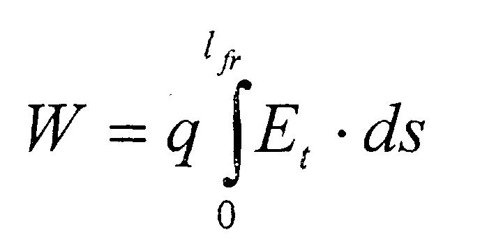
- the tangential component of the electric field strength at the interface between the ceramic and the surrounding medium can accelerate movable electric charges. If the energy absorbed during the mean free path is sufficient to generate further ions in the event of a collision, an avalanche breakdown occurs, which leads to the breakdown of the insulation as a rollover. It is therefore important to minimize the energy W transferred to a free charge q by the tangential component of the electric field strength E t along the surface of the ceramic over the mean free path length I fr :
- edges of the metal cladding are none are sharply defined limits, only an estimate is made here by the maximum of the tangential component and the local value of the tangential component in a distance of 20 ⁇ m from the metallization edge is determined.
- the tangential component of the electric field strength reaches Distance of 20 ⁇ m of the respective metallization edges (3 or 6) the same value. This can reduce the tangential component of the electric field strength in close proximity to the metallization edge (3) of about 20% compared to the level of Technology (Fig. 3) can be achieved and thus also the insulation strength of the basic insulation of the entire substrate can be increased accordingly.
- FIG. 8 shows the results of the inventive optimization method for a Application example according to Fig. 6.
- the optimization process for searching for that Distance e of the edge (62) of the metallic lamination (52) from the edge (61) of the metallic lamination (51), given c 1mm of the edge (32) of the metallic lamination (22) to the edge (32) of the metallic lamination (21) and under assuming that the edge (31) of the metal lamination (21) and the edge (61) of the Metal lamination (51) have the same distance from the edge (8) of the ceramic (1), assumes the same assumptions as mentioned in FIG. 7.
- the metallic lamination (21) is for a sensor surrounded by further metallic laminations (22).
- the corresponding Metal claddings (52) of the second surface (7) are accordingly spaced e - c opposite the edge of the laminations (22) of the first surface (4) set back.
Landscapes
- Engineering & Computer Science (AREA)
- Microelectronics & Electronic Packaging (AREA)
- Cooling Or The Like Of Semiconductors Or Solid State Devices (AREA)
- Structure Of Printed Boards (AREA)
- Thyristors (AREA)
Abstract
Description
| Schicht | Material | Dicke | relative Dielektrizitätskonstante ε/ε0 |
| Metallkaschierung (2, 21, 22) der ersten Oberfläche (4) | Kupfer | 0,3 mm | ---- |
| Keramik (1) | Aluminiumnitrit | 1,0 mm | 9,0 |
| Metallkaschierung (5, 51, 52) der zweiten Oberfläche (7) | Kupfer | 0,3 mm | ---- |
| Umgebungsmedium (9) | Silikonkautschuk | ---- | 2,9 |
Claims (8)
- Leistungshalbleitermodul mit oder ohne Grundplatte bestehend aus einem Gehäuse, zur Kontaktierung benötigten Anschlusselementen, mindestens einem Halbleiterbauelement sowie einem beidseitig metallkaschierten keramischen Substrat, wobei
die metallische Kaschierung (2 bzw. 5) die erste (4) bzw. zweite (7) Oberfläche der Keramik (1) nur teilweise bedeckt, der Abstand des Metallisierungsrandes (3) der ersten auf hohem Potential liegenden metallischen Kaschierung (2) zum Rand (8) der Keramik kleiner ist als der Abstand des Metallisierungsrandes (6) der zweiten metallischen Kaschierung (5) zum Rand (8) der Keramik und dies als Erhöhung der Isolationsfestigkeit der Basisisolierung des Substrats wirkt. - Leistungshalbleitermodul mit oder ohne Grundplatte bestehend aus einem Gehäuse, zur Kontaktierung benötigten Anschlusselementen, mindestens einem Halbleiterbauelement sowie einem beidseitig metallkaschierten keramischen Substrat, wobei
die metallischen Kaschierungen (21, 22 bzw. 52) die erste (4) bzw. zweite (7) Oberfläche der Keramik (1) nur teilweise bedecken, mindestens eine metallische Kaschierung (22) mit einem Rand (32) auf höherem Potential gegenüber mindestens einer weiteren benachbart angeordneten metallischen Kaschierung (21) mit den Rändern (30 und 31) liegt und auf der zweiten Oberfläche (7) der Keramik (1) mindestens eine metallische Kaschierung (52) angeordnet ist, deren Rand (62) gegenüber dem Rand (32) der darüber auf der ersten Oberfläche (4) angeordneten metallischen Kaschierung (22) derart versetzt ist, dass sich unterhalb des Randbereiches dieser metallischen Kaschierung (22) der ersten Oberfläche (4) ein unkaschierter Bereich (e ― c) ergibt und dies eine Erhöhung der Isolationsfestigkeit der Basisisolierung des Substrats bewirkt. - Leistungshalbleitermodul nach Anspruch 1 oder 2, dadurch gekennzeichnet, dass
das keramische Substrat (1) aus Aluminiumoxid, Aluminiumnitrit, Berylliumoxid oder Siliziumnitrit besteht. - Leistungshalbleitermodut nach Anspruch 1 oder 2, dadurch gekennzeichnet, dass
die metallische Kaschierung (2, 21, 22, 5, 51, 52) der ersten (4) und der zweiten (7) Oberfläche aus Kupfer, Aluminium oder Silber besteht. - Leistungshalbleitermodul nach Anspruch 1 oder 2, dadurch gekennzeichnet, dass
die metallische Kaschierung (2, 21, 22, 5, 51, 52) der ersten (4) und der zweiten (7) Oberfläche aus unterschiedlichen Metallen besteht - Leistungshalbleitermodul nach Anspruch 1 oder 2, dadurch gekennzeichnet, dass
die metallische Kaschierung (2, 21, 22, 5, 51, 52) der ersten (4) und der zweiten (7) Oberfläche aus mehreren Metallschichten und unterschiedlichen Metallen besteht. - Leistungshalbleitermodul nach Anspruch 1 oder 2, dadurch gekennzeichnet, dass
die metallische Kaschierung (2, 21, 22, 5, 51, 52) auf dem keramischen Substrat (1) durch des Direct Copper Bonding (DCB) Verfahren oder das Active Metal Brazing (AMB) Verfahren hergestellt ist. - Leistungshalbleitermodul nach Anspruch 2, dadurch gekennzeichnet, dass
auf der zweiten Oberfläche (7) der Keramik (1) eine weitere metallische Kaschierung (51) angeordnet ist, deren Ränder (60, 61) näher am Rand (8) der Keramik (1) angeordnet sind als der Rand (62) der metallischen Kaschierung (62)
Applications Claiming Priority (4)
| Application Number | Priority Date | Filing Date | Title |
|---|---|---|---|
| DE10063714 | 2000-12-20 | ||
| DE10063714A DE10063714C2 (de) | 2000-12-20 | 2000-12-20 | Leistungshalbleitermodul mit hoher Isolationsfestigkeit |
| DE10158185A DE10158185B4 (de) | 2000-12-20 | 2001-11-27 | Leistungshalbleitermodul mit hoher Isolationsfestigkeit |
| DE10158185 | 2001-11-27 |
Publications (3)
| Publication Number | Publication Date |
|---|---|
| EP1217659A2 true EP1217659A2 (de) | 2002-06-26 |
| EP1217659A3 EP1217659A3 (de) | 2005-03-23 |
| EP1217659B1 EP1217659B1 (de) | 2011-05-25 |
Family
ID=26008016
Family Applications (1)
| Application Number | Title | Priority Date | Filing Date |
|---|---|---|---|
| EP01129819A Expired - Lifetime EP1217659B1 (de) | 2000-12-20 | 2001-12-14 | Leistungshalbleitermodul mit hoher Spannungsfestigkeit |
Country Status (5)
| Country | Link |
|---|---|
| US (1) | US6469378B2 (de) |
| EP (1) | EP1217659B1 (de) |
| JP (1) | JP2002270730A (de) |
| AT (1) | ATE511211T1 (de) |
| DE (1) | DE10158185B4 (de) |
Cited By (1)
| Publication number | Priority date | Publication date | Assignee | Title |
|---|---|---|---|---|
| EP3979313A1 (de) * | 2020-09-30 | 2022-04-06 | SEMIKRON Elektronik GmbH & Co. KG | Leistungselektronische einrichtung und leistungshalbleitermodul damit |
Families Citing this family (12)
| Publication number | Priority date | Publication date | Assignee | Title |
|---|---|---|---|---|
| JP3971296B2 (ja) | 2002-12-27 | 2007-09-05 | Dowaホールディングス株式会社 | 金属−セラミックス接合基板およびその製造方法 |
| DE102005046710B4 (de) * | 2005-09-29 | 2012-12-06 | Infineon Technologies Ag | Verfahren zur Herstellung einer Bauelementanordnung mit einem Träger und einem darauf montierten Halbleiterchip |
| DE102009000514A1 (de) * | 2009-01-30 | 2010-08-26 | Robert Bosch Gmbh | Verbundbauteil sowie Verfahren zum Herstellen eines Verbundbauteil |
| DE102012102611B4 (de) * | 2012-02-15 | 2017-07-27 | Rogers Germany Gmbh | Metall-Keramik-Substrat sowie Verfahren zum Herstellen eines Metall-Keramik-Substrates |
| AT514835A1 (de) | 2013-10-04 | 2015-04-15 | Kohlbrat & Bunz Gmbh | Transportmittel mit einer flexiblen Grundplatte |
| CN103633035A (zh) * | 2013-12-04 | 2014-03-12 | 西安永电电气有限责任公司 | 一种igbt模块结构 |
| JP2018026370A (ja) * | 2014-11-13 | 2018-02-15 | 株式会社日立製作所 | パワー半導体モジュール |
| JP6500565B2 (ja) | 2015-04-01 | 2019-04-17 | 富士電機株式会社 | 半導体モジュール |
| JP2017135144A (ja) * | 2016-01-25 | 2017-08-03 | 三菱電機株式会社 | 半導体モジュール |
| TW202106129A (zh) | 2019-03-26 | 2021-02-01 | 日商三菱綜合材料股份有限公司 | 絕緣電路基板 |
| JP7795863B2 (ja) | 2021-02-17 | 2026-01-08 | 富士電機株式会社 | 半導体装置および半導体装置の製造方法 |
| JP7707676B2 (ja) | 2021-06-16 | 2025-07-15 | 富士電機株式会社 | 半導体モジュール |
Family Cites Families (24)
| Publication number | Priority date | Publication date | Assignee | Title |
|---|---|---|---|---|
| FR2524712B1 (fr) * | 1982-03-31 | 1985-06-07 | Radiotechnique Compelec | Circuit hyperfrequence a condensateur integre et application a un circuit d'alimentation |
| US5077595A (en) * | 1990-01-25 | 1991-12-31 | Mitsubishi Denki Kabushiki Kaisha | Semiconductor device |
| JP3199058B2 (ja) * | 1991-10-14 | 2001-08-13 | 富士電機株式会社 | 半導体装置 |
| JP2772184B2 (ja) * | 1991-11-07 | 1998-07-02 | 株式会社東芝 | 半導体装置 |
| JP2656416B2 (ja) * | 1991-12-16 | 1997-09-24 | 三菱電機株式会社 | 半導体装置および半導体装置の製造方法、並びに半導体装置に用いられる複合基板および複合基板の製造方法 |
| JP2838625B2 (ja) * | 1992-09-08 | 1998-12-16 | 株式会社日立製作所 | 半導体モジュール |
| DE4310466A1 (de) * | 1993-03-31 | 1994-10-06 | Klein Schanzlin & Becker Ag | Pumpenstufe in Blechbauweise |
| DE4319944C2 (de) * | 1993-06-03 | 1998-07-23 | Schulz Harder Juergen | Mehrfach-Substrat sowie Verfahren zu seiner Herstellung |
| DE19522173C1 (de) * | 1995-06-19 | 1996-10-17 | Eupec Gmbh & Co Kg | Leistungs-Halbleitermodul |
| EP0789397B1 (de) * | 1996-02-07 | 2004-05-06 | Hitachi, Ltd. | Schaltungsplatine und Halbleiterbauteil mit dieser |
| EP0874399A1 (de) * | 1996-08-20 | 1998-10-28 | Kabushiki Kaisha Toshiba | Siliziumnitrid-leiterplatte und halbleiter-modul |
| JP3512977B2 (ja) * | 1996-08-27 | 2004-03-31 | 同和鉱業株式会社 | 高信頼性半導体用基板 |
| DE19651632C2 (de) * | 1996-12-12 | 2000-12-14 | Semikron Elektronik Gmbh | Leistungshalbleitermodul |
| DE19700963C2 (de) * | 1997-01-14 | 2000-12-21 | Telefunken Microelectron | Verfahren zur Herstellung eines Leistungsmoduls mit einer aktive Halbleiterbauelemente und passive Halbleiterbauelemente aufweisenden Schaltungsanordnung |
| CA2255441C (en) * | 1997-12-08 | 2003-08-05 | Hiroki Sekiya | Package for semiconductor power device and method for assembling the same |
| US6344667B1 (en) * | 1998-03-02 | 2002-02-05 | Kabushiki Kaisha Toshiba | Wiring board with reduced radiation of undesired electromagnetic waves |
| DE69938271T2 (de) * | 1998-05-29 | 2009-03-19 | Kyocera Corp. | Hochfrequenzmodul |
| EP1101248A2 (de) * | 1998-08-05 | 2001-05-23 | Infineon Technologies AG | Substrat für hochspannungsmodule |
| JP4165952B2 (ja) * | 1999-02-26 | 2008-10-15 | 三洋電機株式会社 | 半導体装置 |
| JP2000335983A (ja) * | 1999-05-28 | 2000-12-05 | Denki Kagaku Kogyo Kk | 接合体の製造方法 |
| JP2000340716A (ja) * | 1999-05-31 | 2000-12-08 | Kyocera Corp | 配線基板 |
| DE19959248A1 (de) * | 1999-12-08 | 2001-06-28 | Daimler Chrysler Ag | Isolationsverbesserung bei Hochleistungs-Halbleitermodulen |
| JP3849381B2 (ja) * | 1999-12-20 | 2006-11-22 | 株式会社日立製作所 | 絶縁回路基板の製造方法 |
| DE10063714C2 (de) * | 2000-12-20 | 2002-11-07 | Semikron Elektronik Gmbh | Leistungshalbleitermodul mit hoher Isolationsfestigkeit |
-
2001
- 2001-11-27 DE DE10158185A patent/DE10158185B4/de not_active Expired - Lifetime
- 2001-12-14 EP EP01129819A patent/EP1217659B1/de not_active Expired - Lifetime
- 2001-12-14 AT AT01129819T patent/ATE511211T1/de active
- 2001-12-17 JP JP2001383264A patent/JP2002270730A/ja active Pending
- 2001-12-20 US US10/027,802 patent/US6469378B2/en not_active Expired - Lifetime
Cited By (2)
| Publication number | Priority date | Publication date | Assignee | Title |
|---|---|---|---|---|
| EP3979313A1 (de) * | 2020-09-30 | 2022-04-06 | SEMIKRON Elektronik GmbH & Co. KG | Leistungselektronische einrichtung und leistungshalbleitermodul damit |
| US11967536B2 (en) | 2020-09-30 | 2024-04-23 | Semikron Elektronik Gmbh Co., Kg | Electronic power unit and semiconductor power module |
Also Published As
| Publication number | Publication date |
|---|---|
| EP1217659A3 (de) | 2005-03-23 |
| ATE511211T1 (de) | 2011-06-15 |
| US6469378B2 (en) | 2002-10-22 |
| DE10158185B4 (de) | 2005-08-11 |
| EP1217659B1 (de) | 2011-05-25 |
| JP2002270730A (ja) | 2002-09-20 |
| DE10158185A1 (de) | 2003-07-03 |
| US20020125563A1 (en) | 2002-09-12 |
Similar Documents
| Publication | Publication Date | Title |
|---|---|---|
| DE102014200869B4 (de) | Integrierter Kondensator und Verfahren zum Herstellen desselben und dessen Verwendung | |
| DE10158185B4 (de) | Leistungshalbleitermodul mit hoher Isolationsfestigkeit | |
| DE102014111931B4 (de) | Niederinduktive Schaltungsanordnung mit Laststromsammelleiterbahn | |
| DE3221199C2 (de) | ||
| DE69033229T2 (de) | Anschlussfläche für Halbleiteranordnung | |
| DE69624712T2 (de) | Verfahren zur herstellung einer metall-leitungsstruktur für eine integrierte schaltung mit verbessertem elektromigrationswiderstand | |
| DE102016110742A1 (de) | Filterbauelement zur Filterung eines Störsignals | |
| DE112017006866T5 (de) | Isoliertes wärmeabfuhrsubstrat | |
| DE10063714C2 (de) | Leistungshalbleitermodul mit hoher Isolationsfestigkeit | |
| DE102022109792B4 (de) | Leistungshalbleitermodul | |
| DE102004009296B4 (de) | Verfahren zum Herstellen einer Anordnung eines elektrischen Bauelements | |
| DE102004059389B4 (de) | Halbleiterbauelement mit Ausgleichsmetallisierung | |
| DE19929735A1 (de) | Elektronikkomponente | |
| DE19614501C2 (de) | Verfahren zum Herstellen eines Keramik-Metall-Substrates sowie Keramik-Metall-Substrat | |
| DE112021005798B4 (de) | Schichtkondensator | |
| DE10035170B4 (de) | Keramikkörper mit Temperiervorrichtung, Verfahren zum Herstellen und Verwendung des Keramikkörpers | |
| EP1247250B1 (de) | Chipkartenanordnung | |
| DE69831202T2 (de) | Realisierung eines intermetallischen Kondensators | |
| DE102008026347A1 (de) | Leistungselektronische Anordnung mit einem Substrat und einem Grundkörper | |
| EP1518272B1 (de) | Unter ein pad integrierte halbleiterstruktur | |
| DE102005056906B4 (de) | Integrierte Schaltungsanordnung mit in Reihe geschalteten Kondensatoren und Verwendung | |
| DE102019115573B4 (de) | Leistungselektronische Schalteinrichtung und Verfahren zur Herstellung | |
| EP0665560A2 (de) | Hybridschaltungsanordnung | |
| DE102021003748A1 (de) | Anordnung zur Kühlung eines Hochvoltbauteils | |
| EP3890001A1 (de) | Verfahren zur steigerung der elektrischen funktionalität und/oder lebensdauer von leistungselektronischen modulen |
Legal Events
| Date | Code | Title | Description |
|---|---|---|---|
| PUAI | Public reference made under article 153(3) epc to a published international application that has entered the european phase |
Free format text: ORIGINAL CODE: 0009012 |
|
| AK | Designated contracting states |
Kind code of ref document: A2 Designated state(s): AT BE CH CY DE DK ES FI FR GB GR IE IT LI LU MC NL PT SE TR |
|
| AX | Request for extension of the european patent |
Free format text: AL;LT;LV;MK;RO;SI |
|
| PUAL | Search report despatched |
Free format text: ORIGINAL CODE: 0009013 |
|
| AK | Designated contracting states |
Kind code of ref document: A3 Designated state(s): AT BE CH CY DE DK ES FI FR GB GR IE IT LI LU MC NL PT SE TR |
|
| AX | Request for extension of the european patent |
Extension state: AL LT LV MK RO SI |
|
| 17P | Request for examination filed |
Effective date: 20050214 |
|
| RAP1 | Party data changed (applicant data changed or rights of an application transferred) |
Owner name: SEMIKRON ELEKTRONIK GMBH & CO. KG |
|
| AKX | Designation fees paid |
Designated state(s): AT BE CH CY DE DK ES FI FR GB GR IE IT LI LU MC NL PT SE TR |
|
| 17Q | First examination report despatched |
Effective date: 20061016 |
|
| GRAP | Despatch of communication of intention to grant a patent |
Free format text: ORIGINAL CODE: EPIDOSNIGR1 |
|
| GRAS | Grant fee paid |
Free format text: ORIGINAL CODE: EPIDOSNIGR3 |
|
| GRAA | (expected) grant |
Free format text: ORIGINAL CODE: 0009210 |
|
| AK | Designated contracting states |
Kind code of ref document: B1 Designated state(s): AT BE CH CY DE DK ES FI FR GB GR IE IT LI LU MC NL PT SE TR |
|
| REG | Reference to a national code |
Ref country code: GB Ref legal event code: FG4D Free format text: NOT ENGLISH |
|
| REG | Reference to a national code |
Ref country code: CH Ref legal event code: EP |
|
| REG | Reference to a national code |
Ref country code: IE Ref legal event code: FG4D Free format text: LANGUAGE OF EP DOCUMENT: GERMAN |
|
| REG | Reference to a national code |
Ref country code: DE Ref legal event code: R096 Ref document number: 50115894 Country of ref document: DE Effective date: 20110707 |
|
| REG | Reference to a national code |
Ref country code: CH Ref legal event code: NV Representative=s name: BRAUNPAT BRAUN EDER AG |
|
| REG | Reference to a national code |
Ref country code: NL Ref legal event code: VDEP Effective date: 20110525 |
|
| PG25 | Lapsed in a contracting state [announced via postgrant information from national office to epo] |
Ref country code: SE Free format text: LAPSE BECAUSE OF FAILURE TO SUBMIT A TRANSLATION OF THE DESCRIPTION OR TO PAY THE FEE WITHIN THE PRESCRIBED TIME-LIMIT Effective date: 20110525 Ref country code: PT Free format text: LAPSE BECAUSE OF FAILURE TO SUBMIT A TRANSLATION OF THE DESCRIPTION OR TO PAY THE FEE WITHIN THE PRESCRIBED TIME-LIMIT Effective date: 20110926 |
|
| PG25 | Lapsed in a contracting state [announced via postgrant information from national office to epo] |
Ref country code: CY Free format text: LAPSE BECAUSE OF FAILURE TO SUBMIT A TRANSLATION OF THE DESCRIPTION OR TO PAY THE FEE WITHIN THE PRESCRIBED TIME-LIMIT Effective date: 20110525 Ref country code: FI Free format text: LAPSE BECAUSE OF FAILURE TO SUBMIT A TRANSLATION OF THE DESCRIPTION OR TO PAY THE FEE WITHIN THE PRESCRIBED TIME-LIMIT Effective date: 20110525 Ref country code: ES Free format text: LAPSE BECAUSE OF FAILURE TO SUBMIT A TRANSLATION OF THE DESCRIPTION OR TO PAY THE FEE WITHIN THE PRESCRIBED TIME-LIMIT Effective date: 20110905 Ref country code: GR Free format text: LAPSE BECAUSE OF FAILURE TO SUBMIT A TRANSLATION OF THE DESCRIPTION OR TO PAY THE FEE WITHIN THE PRESCRIBED TIME-LIMIT Effective date: 20110826 |
|
| REG | Reference to a national code |
Ref country code: IE Ref legal event code: FD4D |
|
| PG25 | Lapsed in a contracting state [announced via postgrant information from national office to epo] |
Ref country code: NL Free format text: LAPSE BECAUSE OF FAILURE TO SUBMIT A TRANSLATION OF THE DESCRIPTION OR TO PAY THE FEE WITHIN THE PRESCRIBED TIME-LIMIT Effective date: 20110525 |
|
| PG25 | Lapsed in a contracting state [announced via postgrant information from national office to epo] |
Ref country code: IE Free format text: LAPSE BECAUSE OF FAILURE TO SUBMIT A TRANSLATION OF THE DESCRIPTION OR TO PAY THE FEE WITHIN THE PRESCRIBED TIME-LIMIT Effective date: 20110525 |
|
| PG25 | Lapsed in a contracting state [announced via postgrant information from national office to epo] |
Ref country code: DK Free format text: LAPSE BECAUSE OF FAILURE TO SUBMIT A TRANSLATION OF THE DESCRIPTION OR TO PAY THE FEE WITHIN THE PRESCRIBED TIME-LIMIT Effective date: 20110525 |
|
| PLBE | No opposition filed within time limit |
Free format text: ORIGINAL CODE: 0009261 |
|
| STAA | Information on the status of an ep patent application or granted ep patent |
Free format text: STATUS: NO OPPOSITION FILED WITHIN TIME LIMIT |
|
| 26N | No opposition filed |
Effective date: 20120228 |
|
| PG25 | Lapsed in a contracting state [announced via postgrant information from national office to epo] |
Ref country code: IT Free format text: LAPSE BECAUSE OF FAILURE TO SUBMIT A TRANSLATION OF THE DESCRIPTION OR TO PAY THE FEE WITHIN THE PRESCRIBED TIME-LIMIT Effective date: 20110525 |
|
| REG | Reference to a national code |
Ref country code: DE Ref legal event code: R097 Ref document number: 50115894 Country of ref document: DE Effective date: 20120228 |
|
| BERE | Be: lapsed |
Owner name: SEMIKRON ELEKTRONIK G.M.B.H. & CO. KG Effective date: 20111231 |
|
| PG25 | Lapsed in a contracting state [announced via postgrant information from national office to epo] |
Ref country code: MC Free format text: LAPSE BECAUSE OF NON-PAYMENT OF DUE FEES Effective date: 20111231 |
|
| PG25 | Lapsed in a contracting state [announced via postgrant information from national office to epo] |
Ref country code: BE Free format text: LAPSE BECAUSE OF NON-PAYMENT OF DUE FEES Effective date: 20111231 |
|
| REG | Reference to a national code |
Ref country code: AT Ref legal event code: MM01 Ref document number: 511211 Country of ref document: AT Kind code of ref document: T Effective date: 20111214 |
|
| PG25 | Lapsed in a contracting state [announced via postgrant information from national office to epo] |
Ref country code: LU Free format text: LAPSE BECAUSE OF NON-PAYMENT OF DUE FEES Effective date: 20111214 |
|
| PG25 | Lapsed in a contracting state [announced via postgrant information from national office to epo] |
Ref country code: AT Free format text: LAPSE BECAUSE OF NON-PAYMENT OF DUE FEES Effective date: 20111214 |
|
| PG25 | Lapsed in a contracting state [announced via postgrant information from national office to epo] |
Ref country code: TR Free format text: LAPSE BECAUSE OF FAILURE TO SUBMIT A TRANSLATION OF THE DESCRIPTION OR TO PAY THE FEE WITHIN THE PRESCRIBED TIME-LIMIT Effective date: 20110525 |
|
| REG | Reference to a national code |
Ref country code: FR Ref legal event code: PLFP Year of fee payment: 15 |
|
| REG | Reference to a national code |
Ref country code: FR Ref legal event code: PLFP Year of fee payment: 16 |
|
| REG | Reference to a national code |
Ref country code: FR Ref legal event code: PLFP Year of fee payment: 17 |
|
| REG | Reference to a national code |
Ref country code: CH Ref legal event code: PCAR Free format text: NEW ADDRESS: HOLEESTRASSE 87, 4054 BASEL (CH) |
|
| PGFP | Annual fee paid to national office [announced via postgrant information from national office to epo] |
Ref country code: CH Payment date: 20201222 Year of fee payment: 20 Ref country code: FR Payment date: 20201218 Year of fee payment: 20 Ref country code: GB Payment date: 20201222 Year of fee payment: 20 |
|
| PGFP | Annual fee paid to national office [announced via postgrant information from national office to epo] |
Ref country code: DE Payment date: 20201231 Year of fee payment: 20 |
|
| REG | Reference to a national code |
Ref country code: DE Ref legal event code: R071 Ref document number: 50115894 Country of ref document: DE |
|
| REG | Reference to a national code |
Ref country code: CH Ref legal event code: PL |
|
| REG | Reference to a national code |
Ref country code: GB Ref legal event code: PE20 Expiry date: 20211213 |
|
| PG25 | Lapsed in a contracting state [announced via postgrant information from national office to epo] |
Ref country code: GB Free format text: LAPSE BECAUSE OF EXPIRATION OF PROTECTION Effective date: 20211213 |