EP1197825A2 - Integrierte Schaltung mit Schaltungsstellen mit unterschiedlicher Versorgungsspannung - Google Patents
Integrierte Schaltung mit Schaltungsstellen mit unterschiedlicher Versorgungsspannung Download PDFInfo
- Publication number
- EP1197825A2 EP1197825A2 EP01121398A EP01121398A EP1197825A2 EP 1197825 A2 EP1197825 A2 EP 1197825A2 EP 01121398 A EP01121398 A EP 01121398A EP 01121398 A EP01121398 A EP 01121398A EP 1197825 A2 EP1197825 A2 EP 1197825A2
- Authority
- EP
- European Patent Office
- Prior art keywords
- supply voltage
- voltage
- circuit
- resistance
- voltage divider
- Prior art date
- Legal status (The legal status is an assumption and is not a legal conclusion. Google has not performed a legal analysis and makes no representation as to the accuracy of the status listed.)
- Granted
Links
Images
Classifications
-
- G—PHYSICS
- G05—CONTROLLING; REGULATING
- G05F—SYSTEMS FOR REGULATING ELECTRIC OR MAGNETIC VARIABLES
- G05F1/00—Automatic systems in which deviations of an electric quantity from one or more predetermined values are detected at the output of the system and fed back to a device within the system to restore the detected quantity to its predetermined value or values, i.e. retroactive systems
- G05F1/10—Regulating voltage or current
- G05F1/46—Regulating voltage or current wherein the variable actually regulated by the final control device is DC
- G05F1/462—Regulating voltage or current wherein the variable actually regulated by the final control device is DC as a function of the requirements of the load, e.g. delay, temperature, specific voltage/current characteristic
- G05F1/465—Internal voltage generators for integrated circuits, e.g. step down generators
-
- G—PHYSICS
- G05—CONTROLLING; REGULATING
- G05F—SYSTEMS FOR REGULATING ELECTRIC OR MAGNETIC VARIABLES
- G05F3/00—Non-retroactive systems for regulating electric variables by using an uncontrolled element, or an uncontrolled combination of elements, such element or such combination having self-regulating properties
- G05F3/02—Regulating voltage or current
- G05F3/08—Regulating voltage or current wherein the variable is DC
- G05F3/10—Regulating voltage or current wherein the variable is DC using uncontrolled devices with non-linear characteristics
- G05F3/16—Regulating voltage or current wherein the variable is DC using uncontrolled devices with non-linear characteristics being semiconductor devices
- G05F3/20—Regulating voltage or current wherein the variable is DC using uncontrolled devices with non-linear characteristics being semiconductor devices using diode- transistor combinations
- G05F3/24—Regulating voltage or current wherein the variable is DC using uncontrolled devices with non-linear characteristics being semiconductor devices using diode- transistor combinations wherein the transistors are of the field-effect type only
- G05F3/242—Regulating voltage or current wherein the variable is DC using uncontrolled devices with non-linear characteristics being semiconductor devices using diode- transistor combinations wherein the transistors are of the field-effect type only with compensation for device parameters, e.g. channel width modulation, threshold voltage, processing, or external variations, e.g. temperature, loading, supply voltage
- G05F3/247—Regulating voltage or current wherein the variable is DC using uncontrolled devices with non-linear characteristics being semiconductor devices using diode- transistor combinations wherein the transistors are of the field-effect type only with compensation for device parameters, e.g. channel width modulation, threshold voltage, processing, or external variations, e.g. temperature, loading, supply voltage producing a voltage or current as a predetermined function of the supply voltage
Definitions
- the invention relates to an integrated circuit (IC) with first circuit parts whose supply voltage is the same the external supply voltage of the IC and with second Circuit parts whose supply voltage is less than that external supply voltage and as internal supply voltage is derived from the former.
- IC integrated circuit
- Such integrated circuits are known.
- Those Circuit parts, the above as the first circuit parts were made up of large structures that are usually arranged in the periphery and with the external power supply normally working from 5V.
- Those circuit parts that are described above as second circuit parts are primarily logic circuits, those for reasons of higher signal processing speed and the lower power loss with a low internal supply voltage of e.g. 3 V work.
- This internal supply voltage is from a controller not appearing to the outside.
- the latter comprises a reference element, e.g. a zener diode or a bandgap structure, a negative feedback, compensated Control amplifier and external backup capacitors, is So relatively complex and provides the internal supply voltage after switching on the external supply voltage with one caused by the external support capacitors Delay available.
- the invention has for its object an integrated To create a circuit of the type specified in the introduction, the circuit structures to be integrated with less effort and the internal supply voltage without external components almost instantly after application the external supply voltage.
- This task is in an integrated circuit in the Preamble of claim 1 specified genus according to the invention through a supplying the internal supply voltage, Active voltage divider solved the first resistance voltage divider between the supply voltage connection and the reference potential with a downstream impedance converter and a circuit for load-dependent control the partial voltage at the tap of the first resistance voltage divider includes.
- the impedance converter can have an intermediate the supply voltage connection and an internal supply voltage point of the second circuit parts Drain-source path of a first MOSFET, the gate with the tap of the first resistance voltage divider is connected (claim 2).
- the circuit for load-dependent control of the partial voltage at the tap of the first resistance voltage divider can in particular one between the supply voltage connection and drain-source path located at the internal supply voltage point of a second MOSFET, the gate of which a tap of a second resistance voltage divider between the supply voltage connection and the reference potential connected to one in the drain branch of the second MOSFET lying third MOSFET, which is connected to a fourth, between the supply voltage connection and the tap of the first resistor voltage divider lying one Current mirror circuit forms (claim 3).
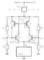
- the drawing shows the simplified diagram of the one Part of an integrated circuit that is used to obtain a internal supply voltage according to the present proposal serves.
- the integrated circuit lying at a reference potential receives the usual external supply voltage via a connection pad of + 5 V and includes not shown first circuit parts whose supply voltage is the same this external supply voltage.
- the integrated Circuitry further includes that designated by "logic" Block symbolized second circuit parts that are used for Achieve a higher signal processing speed and to save power loss with an internal Supply voltage of e.g. +3 V work.
- the circuit shown in detail is used to obtain this internal supply voltage. It comprises a first resistance voltage divider R1, R2 between the supply voltage connection pad and the reference potential.
- the tap X of this first resistance voltage divider R1 is connected to the gate of a first MOSFET structure T1, the drain / source path of which lies between the pad and the supply voltage point of the second circuit parts designated "logic".
- T1 acts as an impedance converter.
- the voltage at the tap X can be, for example, 4.2 V if the gate / source voltage V THN is approximately 1.2 V, thus above the drain / source path drop 2 V. This voltage drop increases as the power consumption of the second circuit parts increases.
- the drain / source path of a second MOSFET structure T1 lies between the supply voltage connection pad and the internal supply voltage point, the gate of which has a tap X' of a second resistance voltage divider R1 ', R2' between the supply voltage connection Pad and the Reference potential is connected.
- the drain branch of the second MOSFET T1 ' is the source / drain path of a third MOSFET structure T2', the gate of which is connected on the one hand to the drain terminal of the second MOSFET T1 and on the other hand to the gate of a fourth MOSFET structure T2
- the drain / Source path is parallel to the partial resistance R1 of the first resistance voltage divider R1, R2.
- the gate / source voltage V THp for the example considered here is approximately 0.9 V.
Landscapes
- Engineering & Computer Science (AREA)
- Microelectronics & Electronic Packaging (AREA)
- Physics & Mathematics (AREA)
- Electromagnetism (AREA)
- General Physics & Mathematics (AREA)
- Radar, Positioning & Navigation (AREA)
- Automation & Control Theory (AREA)
- Control Of Electrical Variables (AREA)
- Semiconductor Integrated Circuits (AREA)
- Logic Circuits (AREA)
- Continuous-Control Power Sources That Use Transistors (AREA)
- Control Of Voltage And Current In General (AREA)
Abstract
- einen ersten Widerstandsspannungsteiler (R1, R2) zwischen dem Versorgungsspannungsanschluß (Pad) und dem Bezugspotential
- einen dem ersten Widerstandspannungsteiler nachgeschalteten Impedanzwandler (T1)
- eine Schaltung zur lastabhängigen Steuerung der Teilspannung am Abgriff (X) des ersten Widerstandsspannungsteilers (R1, R2).
Description
Claims (3)
- Integrierte Schaltung (IC) mit ersten Schaltungsteilen, deren Versorgungsspannung gleich der äußeren Versorgungsspannung des ICs ist und mit zweiten Schaltungsteilen, deren Versorgungsspannung kleiner als die äußere Versorgungsspannung und als interne Versorgungsspannung von ersterer abgeleitet ist,
gekennzeichnet durch
einen die interne Versorgungsspannung liefernden, aktiven Spannungsteiler, der folgendes umfaßteinen ersten Widerstandsspannungsteiler (R1, R2) zwischen dem Versorgungsspannungsanschluß (Pad) und dem Bezugspotentialeinen dem ersten Widerstandspannungsteiler nachgeschalteten Impedanzwandler (T1)eine Schaltung zur lastabhängigen Steuerung der Teilspannung am Abgriff (X) des ersten Widerstandsspannungsteilers (R1, R2). - Schaltung nach Anspruch 1, dadurch gekennzeichnet, daß der Impedanzwandler eine zwischen dem Versorgungsspannungsanschluß (Pad) und einem internen Versorgungsspannungspunkt der zweiten Schaltungsteile liegende Drain/Source-Strecke eines ersten MOSFET (T1) ist, dessen Gate mit dem Abgriff (X) des ersten Widerstandsspannungsteilers (R1, R2) verbunden ist.
- Schaltung nach Anspruch 1 oder 2, dadurch gekennzeichnet, daß die Schaltung zur lastabhängigen Steuerung der Teilspannung am Abgriff (X) des ersten Widerstandsspannungsteilers (R1, R2) folgendes umfaßt:eine zwischen dem Versorgungsspannungsanschluß (Pad) und dem internen Versorgungsspannungspunkt liegende Drain/Source-Strecke eines zweiten MOSFET (T1'), dessen Gate mit einem Abgriff (X') eines zweiten Widerstandsspannungteilers (R1', R2') zwischen dem Versorgungsspannungsanschluß (Pad) und dem Bezugspotential verbunden isteinen im Drainzweig des zweiten MOSFET (T1') liegenden dritten MOSFET (T2'), der mit einem vierten, zwischen dem Versorgungsspannungsanschluß (Pad) und dem Abgriff (X) des ersten Widerstandsspannungsteilers (R1, R2) liegenden MOSFET (T2) eine Stromspiegelschaltung bildet.
Applications Claiming Priority (2)
| Application Number | Priority Date | Filing Date | Title |
|---|---|---|---|
| DE10050561 | 2000-10-12 | ||
| DE10050561A DE10050561B4 (de) | 2000-10-12 | 2000-10-12 | Integrierte Schaltung mit Schaltungsteilen mit unterschiedlicher Versorgungsspannung |
Publications (3)
| Publication Number | Publication Date |
|---|---|
| EP1197825A2 true EP1197825A2 (de) | 2002-04-17 |
| EP1197825A3 EP1197825A3 (de) | 2004-07-07 |
| EP1197825B1 EP1197825B1 (de) | 2009-05-27 |
Family
ID=7659544
Family Applications (1)
| Application Number | Title | Priority Date | Filing Date |
|---|---|---|---|
| EP01121398A Expired - Lifetime EP1197825B1 (de) | 2000-10-12 | 2001-09-06 | Integrierte Schaltung mit Schaltungsstellen mit unterschiedlicher Versorgungsspannung |
Country Status (6)
| Country | Link |
|---|---|
| US (1) | US6605833B2 (de) |
| EP (1) | EP1197825B1 (de) |
| JP (1) | JP2002185302A (de) |
| AT (1) | ATE432491T1 (de) |
| DE (2) | DE10050561B4 (de) |
| HK (1) | HK1048671A1 (de) |
Cited By (1)
| Publication number | Priority date | Publication date | Assignee | Title |
|---|---|---|---|---|
| EP1369762A1 (de) * | 2002-05-29 | 2003-12-10 | Dialog Semiconductor GmbH | Aktives Teilnehmerinformationsmodule |
Families Citing this family (1)
| Publication number | Priority date | Publication date | Assignee | Title |
|---|---|---|---|---|
| US7602019B2 (en) * | 2006-04-20 | 2009-10-13 | Texas Instruments Incorporated | Drive circuit and drain extended transistor for use therein |
Family Cites Families (16)
| Publication number | Priority date | Publication date | Assignee | Title |
|---|---|---|---|---|
| GB2020437B (en) * | 1978-04-14 | 1982-08-04 | Seiko Instr & Electronics | Voltage detecting circuit |
| US4672246A (en) * | 1986-03-10 | 1987-06-09 | Honeywell Inc. | Low offset MOSFET transistor switch control |
| DE3706907C2 (de) * | 1987-03-04 | 1996-09-12 | Bosch Gmbh Robert | Spannungsreglervorstufe mit geringem Spannungsverlust sowie Spannungsregler mit einer solchen Vorstufe |
| NL8900050A (nl) * | 1989-01-10 | 1990-08-01 | Philips Nv | Inrichting voor het meten van een ruststroom van een geintegreerde monolitische digitale schakeling, geintegreerde monolitische digitale schakeling voorzien van een dergelijke inrichting en testapparaat voorzien van een dergelijke inrichting. |
| JP2883625B2 (ja) * | 1989-03-30 | 1999-04-19 | 株式会社東芝 | Mos型充電回路 |
| JPH087636B2 (ja) * | 1990-01-18 | 1996-01-29 | シャープ株式会社 | 半導体装置の電圧降下回路 |
| KR920010633A (ko) * | 1990-11-30 | 1992-06-26 | 김광호 | 반도체 메모리 장치의 기준전압 발생회로 |
| GB2262675A (en) * | 1991-12-20 | 1993-06-23 | Codex Corp | Comparator start-up arrangement |
| US5589794A (en) * | 1994-12-20 | 1996-12-31 | Sgs-Thomson Microelectronics, Inc. | Dynamically controlled voltage reference circuit |
| US5815040A (en) * | 1996-12-30 | 1998-09-29 | Anthony T. Barbetta | Wide bandwidth, current sharing, MOSFET audio power amplifier with multiple feedback loops |
| US6097632A (en) * | 1997-04-18 | 2000-08-01 | Micron Technology, Inc. | Source regulation circuit for an erase operation of flash memory |
| JP3087838B2 (ja) * | 1997-08-05 | 2000-09-11 | 日本電気株式会社 | 定電圧発生回路 |
| US6160440A (en) * | 1998-09-25 | 2000-12-12 | Intel Corporation | Scaleable charge pump for use with a low voltage power supply |
| JP2000331490A (ja) * | 1999-05-18 | 2000-11-30 | Hitachi Ltd | 半導体集積回路装置 |
| JP3278635B2 (ja) * | 1999-05-27 | 2002-04-30 | 沖電気工業株式会社 | 半導体集積回路 |
| US6304131B1 (en) * | 2000-02-22 | 2001-10-16 | Texas Instruments Incorporated | High power supply ripple rejection internally compensated low drop-out voltage regulator using PMOS pass device |
-
2000
- 2000-10-12 DE DE10050561A patent/DE10050561B4/de not_active Expired - Fee Related
-
2001
- 2001-09-06 EP EP01121398A patent/EP1197825B1/de not_active Expired - Lifetime
- 2001-09-06 AT AT01121398T patent/ATE432491T1/de not_active IP Right Cessation
- 2001-09-06 DE DE50114910T patent/DE50114910D1/de not_active Expired - Lifetime
- 2001-09-20 JP JP2001287045A patent/JP2002185302A/ja active Pending
- 2001-10-11 US US09/975,617 patent/US6605833B2/en not_active Expired - Lifetime
-
2002
- 2002-10-17 HK HK02107542.6A patent/HK1048671A1/zh unknown
Cited By (2)
| Publication number | Priority date | Publication date | Assignee | Title |
|---|---|---|---|---|
| EP1369762A1 (de) * | 2002-05-29 | 2003-12-10 | Dialog Semiconductor GmbH | Aktives Teilnehmerinformationsmodule |
| US6952596B2 (en) | 2002-05-29 | 2005-10-04 | Dialog Semiconductor Gmbh | Active subscriber information module |
Also Published As
| Publication number | Publication date |
|---|---|
| DE50114910D1 (de) | 2009-07-09 |
| HK1048671A1 (zh) | 2003-04-11 |
| JP2002185302A (ja) | 2002-06-28 |
| EP1197825B1 (de) | 2009-05-27 |
| ATE432491T1 (de) | 2009-06-15 |
| DE10050561B4 (de) | 2005-04-28 |
| US6605833B2 (en) | 2003-08-12 |
| DE10050561A1 (de) | 2002-05-16 |
| EP1197825A3 (de) | 2004-07-07 |
| US20020043670A1 (en) | 2002-04-18 |
Similar Documents
| Publication | Publication Date | Title |
|---|---|---|
| DE102008059853B4 (de) | Schaltungsanordnung mit einem Lasttransistor und einem Messtransistor | |
| DE69123538T2 (de) | Einschalt-Rücksetzschaltung | |
| DE10110273A1 (de) | Spannungsgenerator mit Standby-Betriebsart | |
| DE3128732A1 (de) | "spannungsdifferenzdetektorschaltung" | |
| DE19982963B4 (de) | Dynamische Vorspannungsschaltung, die eine frühe Spannungsklemmschaltung und translineare Techniken benutzt | |
| DE3323446A1 (de) | Eingangssignalpegelwandler fuer eine mos-digitalschaltung | |
| DE102004055452B4 (de) | Ausgangsschaltung | |
| DE19729480A1 (de) | Kapazitives Netzteil | |
| DE69309337T2 (de) | Komparatorschaltung mit Eingangssignaldämpfungsglied | |
| DE19521663A1 (de) | Integrierter Schaltkreis mit Spannungsregelschaltung | |
| EP1197825B1 (de) | Integrierte Schaltung mit Schaltungsstellen mit unterschiedlicher Versorgungsspannung | |
| DE8912984U1 (de) | Schnittstellenschaltung zwischen zwei an unterschiedlichen Betriebsspannungen betriebenen elektrischen Schaltungen | |
| DE19741430A1 (de) | Schaltungsanordnung und Verfahren zur Unterdrückung störender Rückwirkungen eines Umrichters | |
| EP0280261A2 (de) | Schaltung zur Gewinnung eines temperaturunabhängigen Rechtecksignals aus einem Messsignal | |
| DE10314514B4 (de) | Leistungsvorrichtungssteuerschaltung | |
| DE3133746A1 (de) | "festkoerper-leistungsregler mit ein-aus-anzeige" | |
| DE4434792C1 (de) | Integrierte, in einem ersten und einem zweiten Betriebsmodus betreibbare Schaltungsanordnung | |
| DE4101492A1 (de) | Stromdetektor | |
| EP0748047A1 (de) | Integrierte Pufferschaltung | |
| EP1078460A1 (de) | Verfahren und vorrichtung zum umschalten eines feldeffekttransistors | |
| DE19755130C1 (de) | Pufferschaltung | |
| DE102018116669B4 (de) | Verfahren zum Betrieb eines stützkondensatorfreien Low-Drop-Spannungsreglers mit großem Spannungsbereich | |
| DE69713266T2 (de) | Oszillator mit einer startschaltung | |
| DE10349629A1 (de) | Elektronischer Schaltkreis | |
| DE102019116700B4 (de) | Stützkondensatorfreier Low-Drop-Spannungsregler mit großem Spannungsbereich mit einem DIMOS Transistor und Verfahren zu dessen Betrieb |
Legal Events
| Date | Code | Title | Description |
|---|---|---|---|
| PUAI | Public reference made under article 153(3) epc to a published international application that has entered the european phase |
Free format text: ORIGINAL CODE: 0009012 |
|
| AK | Designated contracting states |
Kind code of ref document: A2 Designated state(s): AT BE CH CY DE DK ES FI FR GB GR IE IT LI LU MC NL PT SE TR |
|
| AX | Request for extension of the european patent |
Free format text: AL;LT;LV;MK;RO;SI |
|
| PUAL | Search report despatched |
Free format text: ORIGINAL CODE: 0009013 |
|
| AK | Designated contracting states |
Kind code of ref document: A3 Designated state(s): AT BE CH CY DE DK ES FI FR GB GR IE IT LI LU MC NL PT SE TR |
|
| AX | Request for extension of the european patent |
Extension state: AL LT LV MK RO SI |
|
| 17P | Request for examination filed |
Effective date: 20040715 |
|
| AKX | Designation fees paid |
Designated state(s): AT BE CH CY DE DK ES FI FR GB GR IE IT LI LU MC NL PT SE TR |
|
| 17Q | First examination report despatched |
Effective date: 20060703 |
|
| GRAP | Despatch of communication of intention to grant a patent |
Free format text: ORIGINAL CODE: EPIDOSNIGR1 |
|
| GRAS | Grant fee paid |
Free format text: ORIGINAL CODE: EPIDOSNIGR3 |
|
| GRAA | (expected) grant |
Free format text: ORIGINAL CODE: 0009210 |
|
| AK | Designated contracting states |
Kind code of ref document: B1 Designated state(s): AT BE CH CY DE DK ES FI FR GB GR IE IT LI LU MC NL PT SE TR |
|
| REG | Reference to a national code |
Ref country code: GB Ref legal event code: FG4D Free format text: NOT ENGLISH |
|
| REG | Reference to a national code |
Ref country code: CH Ref legal event code: EP |
|
| REG | Reference to a national code |
Ref country code: IE Ref legal event code: FG4D Free format text: LANGUAGE OF EP DOCUMENT: GERMAN |
|
| REF | Corresponds to: |
Ref document number: 50114910 Country of ref document: DE Date of ref document: 20090709 Kind code of ref document: P |
|
| PG25 | Lapsed in a contracting state [announced via postgrant information from national office to epo] |
Ref country code: FI Free format text: LAPSE BECAUSE OF FAILURE TO SUBMIT A TRANSLATION OF THE DESCRIPTION OR TO PAY THE FEE WITHIN THE PRESCRIBED TIME-LIMIT Effective date: 20090527 Ref country code: PT Free format text: LAPSE BECAUSE OF FAILURE TO SUBMIT A TRANSLATION OF THE DESCRIPTION OR TO PAY THE FEE WITHIN THE PRESCRIBED TIME-LIMIT Effective date: 20090927 |
|
| NLV1 | Nl: lapsed or annulled due to failure to fulfill the requirements of art. 29p and 29m of the patents act | ||
| PG25 | Lapsed in a contracting state [announced via postgrant information from national office to epo] |
Ref country code: SE Free format text: LAPSE BECAUSE OF FAILURE TO SUBMIT A TRANSLATION OF THE DESCRIPTION OR TO PAY THE FEE WITHIN THE PRESCRIBED TIME-LIMIT Effective date: 20090827 Ref country code: NL Free format text: LAPSE BECAUSE OF FAILURE TO SUBMIT A TRANSLATION OF THE DESCRIPTION OR TO PAY THE FEE WITHIN THE PRESCRIBED TIME-LIMIT Effective date: 20090527 |
|
| REG | Reference to a national code |
Ref country code: IE Ref legal event code: FD4D |
|
| PG25 | Lapsed in a contracting state [announced via postgrant information from national office to epo] |
Ref country code: DK Free format text: LAPSE BECAUSE OF FAILURE TO SUBMIT A TRANSLATION OF THE DESCRIPTION OR TO PAY THE FEE WITHIN THE PRESCRIBED TIME-LIMIT Effective date: 20090527 Ref country code: ES Free format text: LAPSE BECAUSE OF FAILURE TO SUBMIT A TRANSLATION OF THE DESCRIPTION OR TO PAY THE FEE WITHIN THE PRESCRIBED TIME-LIMIT Effective date: 20090907 Ref country code: IE Free format text: LAPSE BECAUSE OF FAILURE TO SUBMIT A TRANSLATION OF THE DESCRIPTION OR TO PAY THE FEE WITHIN THE PRESCRIBED TIME-LIMIT Effective date: 20090527 |
|
| REG | Reference to a national code |
Ref country code: HK Ref legal event code: WD Ref document number: 1048671 Country of ref document: HK |
|
| BERE | Be: lapsed |
Owner name: DIALOG SEMICONDUCTOR G.M.B.H. Effective date: 20090930 |
|
| PLBE | No opposition filed within time limit |
Free format text: ORIGINAL CODE: 0009261 |
|
| STAA | Information on the status of an ep patent application or granted ep patent |
Free format text: STATUS: NO OPPOSITION FILED WITHIN TIME LIMIT |
|
| PG25 | Lapsed in a contracting state [announced via postgrant information from national office to epo] |
Ref country code: MC Free format text: LAPSE BECAUSE OF NON-PAYMENT OF DUE FEES Effective date: 20090930 |
|
| REG | Reference to a national code |
Ref country code: CH Ref legal event code: PL |
|
| 26N | No opposition filed |
Effective date: 20100302 |
|
| PG25 | Lapsed in a contracting state [announced via postgrant information from national office to epo] |
Ref country code: BE Free format text: LAPSE BECAUSE OF NON-PAYMENT OF DUE FEES Effective date: 20090930 |
|
| PG25 | Lapsed in a contracting state [announced via postgrant information from national office to epo] |
Ref country code: LI Free format text: LAPSE BECAUSE OF NON-PAYMENT OF DUE FEES Effective date: 20090930 Ref country code: GR Free format text: LAPSE BECAUSE OF FAILURE TO SUBMIT A TRANSLATION OF THE DESCRIPTION OR TO PAY THE FEE WITHIN THE PRESCRIBED TIME-LIMIT Effective date: 20090828 Ref country code: CH Free format text: LAPSE BECAUSE OF NON-PAYMENT OF DUE FEES Effective date: 20090930 |
|
| PG25 | Lapsed in a contracting state [announced via postgrant information from national office to epo] |
Ref country code: AT Free format text: LAPSE BECAUSE OF NON-PAYMENT OF DUE FEES Effective date: 20090906 |
|
| PG25 | Lapsed in a contracting state [announced via postgrant information from national office to epo] |
Ref country code: IT Free format text: LAPSE BECAUSE OF FAILURE TO SUBMIT A TRANSLATION OF THE DESCRIPTION OR TO PAY THE FEE WITHIN THE PRESCRIBED TIME-LIMIT Effective date: 20090527 |
|
| PG25 | Lapsed in a contracting state [announced via postgrant information from national office to epo] |
Ref country code: LU Free format text: LAPSE BECAUSE OF NON-PAYMENT OF DUE FEES Effective date: 20090906 |
|
| PG25 | Lapsed in a contracting state [announced via postgrant information from national office to epo] |
Ref country code: TR Free format text: LAPSE BECAUSE OF FAILURE TO SUBMIT A TRANSLATION OF THE DESCRIPTION OR TO PAY THE FEE WITHIN THE PRESCRIBED TIME-LIMIT Effective date: 20090527 |
|
| PG25 | Lapsed in a contracting state [announced via postgrant information from national office to epo] |
Ref country code: CY Free format text: LAPSE BECAUSE OF FAILURE TO SUBMIT A TRANSLATION OF THE DESCRIPTION OR TO PAY THE FEE WITHIN THE PRESCRIBED TIME-LIMIT Effective date: 20090527 |
|
| REG | Reference to a national code |
Ref country code: DE Ref legal event code: R082 Ref document number: 50114910 Country of ref document: DE Representative=s name: PATENTANWAELTE HENKEL, BREUER & PARTNER, DE |
|
| PGFP | Annual fee paid to national office [announced via postgrant information from national office to epo] |
Ref country code: FR Payment date: 20121018 Year of fee payment: 12 |
|
| REG | Reference to a national code |
Ref country code: FR Ref legal event code: ST Effective date: 20140530 |
|
| PG25 | Lapsed in a contracting state [announced via postgrant information from national office to epo] |
Ref country code: FR Free format text: LAPSE BECAUSE OF NON-PAYMENT OF DUE FEES Effective date: 20130930 |
|
| PGFP | Annual fee paid to national office [announced via postgrant information from national office to epo] |
Ref country code: DE Payment date: 20150925 Year of fee payment: 15 Ref country code: GB Payment date: 20150910 Year of fee payment: 15 |
|
| REG | Reference to a national code |
Ref country code: DE Ref legal event code: R119 Ref document number: 50114910 Country of ref document: DE |
|
| GBPC | Gb: european patent ceased through non-payment of renewal fee |
Effective date: 20160906 |
|
| PG25 | Lapsed in a contracting state [announced via postgrant information from national office to epo] |
Ref country code: GB Free format text: LAPSE BECAUSE OF NON-PAYMENT OF DUE FEES Effective date: 20160906 Ref country code: DE Free format text: LAPSE BECAUSE OF NON-PAYMENT OF DUE FEES Effective date: 20170401 |