EP1195455A1 - Plaquette de silicium, procede de determination de la condition dans laquelle est produit un monocristal de silicium et procede de production d'une plaquette de silicium - Google Patents
Plaquette de silicium, procede de determination de la condition dans laquelle est produit un monocristal de silicium et procede de production d'une plaquette de silicium Download PDFInfo
- Publication number
- EP1195455A1 EP1195455A1 EP01901424A EP01901424A EP1195455A1 EP 1195455 A1 EP1195455 A1 EP 1195455A1 EP 01901424 A EP01901424 A EP 01901424A EP 01901424 A EP01901424 A EP 01901424A EP 1195455 A1 EP1195455 A1 EP 1195455A1
- Authority
- EP
- European Patent Office
- Prior art keywords
- silicon
- single crystal
- silicon wafer
- wafer
- silicon single
- Prior art date
- Legal status (The legal status is an assumption and is not a legal conclusion. Google has not performed a legal analysis and makes no representation as to the accuracy of the status listed.)
- Granted
Links
- XUIMIQQOPSSXEZ-UHFFFAOYSA-N Silicon Chemical compound [Si] XUIMIQQOPSSXEZ-UHFFFAOYSA-N 0.000 title claims abstract description 187
- 229910052710 silicon Inorganic materials 0.000 title claims abstract description 187
- 239000010703 silicon Substances 0.000 title claims abstract description 187
- 239000013078 crystal Substances 0.000 title claims abstract description 162
- 238000004519 manufacturing process Methods 0.000 title claims abstract description 58
- 238000000034 method Methods 0.000 title claims abstract description 42
- 235000012431 wafers Nutrition 0.000 claims abstract description 252
- 230000007547 defect Effects 0.000 claims abstract description 141
- IJGRMHOSHXDMSA-UHFFFAOYSA-N Atomic nitrogen Chemical compound N#N IJGRMHOSHXDMSA-UHFFFAOYSA-N 0.000 claims abstract description 94
- 238000010438 heat treatment Methods 0.000 claims abstract description 71
- 229910052757 nitrogen Inorganic materials 0.000 claims abstract description 47
- QVGXLLKOCUKJST-UHFFFAOYSA-N atomic oxygen Chemical compound [O] QVGXLLKOCUKJST-UHFFFAOYSA-N 0.000 claims abstract description 38
- 239000001301 oxygen Substances 0.000 claims abstract description 38
- 229910052760 oxygen Inorganic materials 0.000 claims abstract description 38
- 239000010410 layer Substances 0.000 claims abstract description 21
- 239000002344 surface layer Substances 0.000 claims abstract description 19
- 238000005259 measurement Methods 0.000 claims description 17
- 201000006935 Becker muscular dystrophy Diseases 0.000 claims description 10
- 208000037663 Best vitelliform macular dystrophy Diseases 0.000 claims description 10
- 208000020938 vitelliform macular dystrophy 2 Diseases 0.000 claims description 10
- 230000008859 change Effects 0.000 claims description 8
- 239000007788 liquid Substances 0.000 claims description 7
- 238000000137 annealing Methods 0.000 description 40
- 238000005054 agglomeration Methods 0.000 description 18
- 230000002776 aggregation Effects 0.000 description 18
- 230000015556 catabolic process Effects 0.000 description 17
- 230000000694 effects Effects 0.000 description 14
- XKRFYHLGVUSROY-UHFFFAOYSA-N Argon Chemical compound [Ar] XKRFYHLGVUSROY-UHFFFAOYSA-N 0.000 description 12
- 238000004140 cleaning Methods 0.000 description 10
- 238000011156 evaluation Methods 0.000 description 10
- 238000005247 gettering Methods 0.000 description 7
- KRHYYFGTRYWZRS-UHFFFAOYSA-N Fluorane Chemical compound F KRHYYFGTRYWZRS-UHFFFAOYSA-N 0.000 description 6
- 229910052786 argon Inorganic materials 0.000 description 6
- 238000011161 development Methods 0.000 description 6
- 238000010586 diagram Methods 0.000 description 6
- 238000005530 etching Methods 0.000 description 6
- 238000013461 design Methods 0.000 description 5
- 239000001257 hydrogen Substances 0.000 description 5
- 229910052739 hydrogen Inorganic materials 0.000 description 5
- 238000001556 precipitation Methods 0.000 description 5
- UFHFLCQGNIYNRP-UHFFFAOYSA-N Hydrogen Chemical compound [H][H] UFHFLCQGNIYNRP-UHFFFAOYSA-N 0.000 description 4
- 230000005764 inhibitory process Effects 0.000 description 4
- 239000000203 mixture Substances 0.000 description 4
- 239000002994 raw material Substances 0.000 description 4
- 238000004088 simulation Methods 0.000 description 4
- 238000004458 analytical method Methods 0.000 description 3
- 230000008901 benefit Effects 0.000 description 3
- 230000000052 comparative effect Effects 0.000 description 3
- 238000002474 experimental method Methods 0.000 description 3
- 239000012535 impurity Substances 0.000 description 3
- 230000008569 process Effects 0.000 description 3
- 230000009467 reduction Effects 0.000 description 3
- GRYLNZFGIOXLOG-UHFFFAOYSA-N Nitric acid Chemical compound O[N+]([O-])=O GRYLNZFGIOXLOG-UHFFFAOYSA-N 0.000 description 2
- 238000013459 approach Methods 0.000 description 2
- 239000012300 argon atmosphere Substances 0.000 description 2
- 238000000149 argon plasma sintering Methods 0.000 description 2
- 239000012298 atmosphere Substances 0.000 description 2
- 238000004364 calculation method Methods 0.000 description 2
- 238000012790 confirmation Methods 0.000 description 2
- 230000005684 electric field Effects 0.000 description 2
- 239000007789 gas Substances 0.000 description 2
- 238000005065 mining Methods 0.000 description 2
- 229910017604 nitric acid Inorganic materials 0.000 description 2
- 239000002245 particle Substances 0.000 description 2
- 238000005498 polishing Methods 0.000 description 2
- 238000011160 research Methods 0.000 description 2
- 238000003325 tomography Methods 0.000 description 2
- 238000012546 transfer Methods 0.000 description 2
- VHUUQVKOLVNVRT-UHFFFAOYSA-N Ammonium hydroxide Chemical compound [NH4+].[OH-] VHUUQVKOLVNVRT-UHFFFAOYSA-N 0.000 description 1
- OKTJSMMVPCPJKN-UHFFFAOYSA-N Carbon Chemical compound [C] OKTJSMMVPCPJKN-UHFFFAOYSA-N 0.000 description 1
- 238000012951 Remeasurement Methods 0.000 description 1
- 230000015572 biosynthetic process Effects 0.000 description 1
- 229910052799 carbon Inorganic materials 0.000 description 1
- 238000011109 contamination Methods 0.000 description 1
- 230000001955 cumulated effect Effects 0.000 description 1
- 238000006731 degradation reaction Methods 0.000 description 1
- 238000009826 distribution Methods 0.000 description 1
- 230000008030 elimination Effects 0.000 description 1
- 238000003379 elimination reaction Methods 0.000 description 1
- 229910001385 heavy metal Inorganic materials 0.000 description 1
- 150000002431 hydrogen Chemical class 0.000 description 1
- 239000012212 insulator Substances 0.000 description 1
- 230000010354 integration Effects 0.000 description 1
- 239000000463 material Substances 0.000 description 1
- 238000002844 melting Methods 0.000 description 1
- 230000008018 melting Effects 0.000 description 1
- 238000005457 optimization Methods 0.000 description 1
- 230000003647 oxidation Effects 0.000 description 1
- 238000007254 oxidation reaction Methods 0.000 description 1
- KMUONIBRACKNSN-UHFFFAOYSA-N potassium dichromate Chemical compound [K+].[K+].[O-][Cr](=O)(=O)O[Cr]([O-])(=O)=O KMUONIBRACKNSN-UHFFFAOYSA-N 0.000 description 1
- 239000002244 precipitate Substances 0.000 description 1
- 239000004065 semiconductor Substances 0.000 description 1
- 238000011272 standard treatment Methods 0.000 description 1
- 239000000126 substance Substances 0.000 description 1
- 239000000758 substrate Substances 0.000 description 1
- 238000002076 thermal analysis method Methods 0.000 description 1
- 230000036962 time dependent Effects 0.000 description 1
- 230000001052 transient effect Effects 0.000 description 1
- 238000011282 treatment Methods 0.000 description 1
- ZDHXKXAHOVTTAH-UHFFFAOYSA-N trichlorosilane Chemical compound Cl[SiH](Cl)Cl ZDHXKXAHOVTTAH-UHFFFAOYSA-N 0.000 description 1
- 239000005052 trichlorosilane Substances 0.000 description 1
- 239000011800 void material Substances 0.000 description 1
- XLYOFNOQVPJJNP-UHFFFAOYSA-N water Substances O XLYOFNOQVPJJNP-UHFFFAOYSA-N 0.000 description 1
Images


Classifications
-
- C—CHEMISTRY; METALLURGY
- C30—CRYSTAL GROWTH
- C30B—SINGLE-CRYSTAL GROWTH; UNIDIRECTIONAL SOLIDIFICATION OF EUTECTIC MATERIAL OR UNIDIRECTIONAL DEMIXING OF EUTECTOID MATERIAL; REFINING BY ZONE-MELTING OF MATERIAL; PRODUCTION OF A HOMOGENEOUS POLYCRYSTALLINE MATERIAL WITH DEFINED STRUCTURE; SINGLE CRYSTALS OR HOMOGENEOUS POLYCRYSTALLINE MATERIAL WITH DEFINED STRUCTURE; AFTER-TREATMENT OF SINGLE CRYSTALS OR A HOMOGENEOUS POLYCRYSTALLINE MATERIAL WITH DEFINED STRUCTURE; APPARATUS THEREFOR
- C30B29/00—Single crystals or homogeneous polycrystalline material with defined structure characterised by the material or by their shape
- C30B29/02—Elements
- C30B29/06—Silicon
-
- C—CHEMISTRY; METALLURGY
- C30—CRYSTAL GROWTH
- C30B—SINGLE-CRYSTAL GROWTH; UNIDIRECTIONAL SOLIDIFICATION OF EUTECTIC MATERIAL OR UNIDIRECTIONAL DEMIXING OF EUTECTOID MATERIAL; REFINING BY ZONE-MELTING OF MATERIAL; PRODUCTION OF A HOMOGENEOUS POLYCRYSTALLINE MATERIAL WITH DEFINED STRUCTURE; SINGLE CRYSTALS OR HOMOGENEOUS POLYCRYSTALLINE MATERIAL WITH DEFINED STRUCTURE; AFTER-TREATMENT OF SINGLE CRYSTALS OR A HOMOGENEOUS POLYCRYSTALLINE MATERIAL WITH DEFINED STRUCTURE; APPARATUS THEREFOR
- C30B15/00—Single-crystal growth by pulling from a melt, e.g. Czochralski method
- C30B15/20—Controlling or regulating
- C30B15/203—Controlling or regulating the relationship of pull rate (v) to axial thermal gradient (G)
-
- C—CHEMISTRY; METALLURGY
- C30—CRYSTAL GROWTH
- C30B—SINGLE-CRYSTAL GROWTH; UNIDIRECTIONAL SOLIDIFICATION OF EUTECTIC MATERIAL OR UNIDIRECTIONAL DEMIXING OF EUTECTOID MATERIAL; REFINING BY ZONE-MELTING OF MATERIAL; PRODUCTION OF A HOMOGENEOUS POLYCRYSTALLINE MATERIAL WITH DEFINED STRUCTURE; SINGLE CRYSTALS OR HOMOGENEOUS POLYCRYSTALLINE MATERIAL WITH DEFINED STRUCTURE; AFTER-TREATMENT OF SINGLE CRYSTALS OR A HOMOGENEOUS POLYCRYSTALLINE MATERIAL WITH DEFINED STRUCTURE; APPARATUS THEREFOR
- C30B15/00—Single-crystal growth by pulling from a melt, e.g. Czochralski method
- C30B15/20—Controlling or regulating
- C30B15/206—Controlling or regulating the thermal history of growing the ingot
-
- G—PHYSICS
- G01—MEASURING; TESTING
- G01N—INVESTIGATING OR ANALYSING MATERIALS BY DETERMINING THEIR CHEMICAL OR PHYSICAL PROPERTIES
- G01N33/00—Investigating or analysing materials by specific methods not covered by groups G01N1/00 - G01N31/00
- G01N33/0095—Semiconductive materials
-
- H—ELECTRICITY
- H01—ELECTRIC ELEMENTS
- H01L—SEMICONDUCTOR DEVICES NOT COVERED BY CLASS H10
- H01L21/00—Processes or apparatus adapted for the manufacture or treatment of semiconductor or solid state devices or of parts thereof
- H01L21/02—Manufacture or treatment of semiconductor devices or of parts thereof
- H01L21/04—Manufacture or treatment of semiconductor devices or of parts thereof the devices having potential barriers, e.g. a PN junction, depletion layer or carrier concentration layer
- H01L21/18—Manufacture or treatment of semiconductor devices or of parts thereof the devices having potential barriers, e.g. a PN junction, depletion layer or carrier concentration layer the devices having semiconductor bodies comprising elements of Group IV of the Periodic Table or AIIIBV compounds with or without impurities, e.g. doping materials
- H01L21/30—Treatment of semiconductor bodies using processes or apparatus not provided for in groups H01L21/20 - H01L21/26
- H01L21/322—Treatment of semiconductor bodies using processes or apparatus not provided for in groups H01L21/20 - H01L21/26 to modify their internal properties, e.g. to produce internal imperfections
- H01L21/3221—Treatment of semiconductor bodies using processes or apparatus not provided for in groups H01L21/20 - H01L21/26 to modify their internal properties, e.g. to produce internal imperfections of silicon bodies, e.g. for gettering
- H01L21/3225—Thermally inducing defects using oxygen present in the silicon body for intrinsic gettering
Definitions
- the present invention relates to a silicon wafer having a grown-in defect density lower than that of conventional epitaxial wafers, annealed wafers and wafers having an N-region for entire plane, a method for determining production conditions of the same and a method for producing the same.
- the present invention further relates to a method for determining production conditions of a silicon single crystal that is for stable production of silicon wafers of low grown-in defect density, which wafers are produced by subjecting silicon wafers produced from a nitrogen-doped silicon single crystal to heat treatment, and a method for producing the same.
- wafers produced form of crystals having few grown-in defects including epitaxial wafers consisting a usual silicon wafer on which a silicon layer is newly provided by epitaxial growth, annealed wafers which is produced by subjecting wafers to heat treatments at a high temperature in hydrogen or argon atmospheres, wafers having an N-region (a region free from dislocation clusters existing outside the OSF ring) for entire plane which are produced by improving the growth conditions of CZ-Si single crystals and so forth.
- the wafers obtained by annealing nitrogen-doped wafers are extremely useful as wafers showing reduced grown-in defects in wafer surface layer portions and high density of BMD (Bulk Micro Defect) in bulk portions.
- BMD Bulk Micro Defect
- MO-601 produced by Mitsui Mining and Smelting Co., Ltd.
- MO-601 is a highly precise defect evaluation apparatus, which can measure even extremely fine defects having a size of about 50 nm, and also has a function enabling evaluation of defects along the depth direction for a depth of 5 ⁇ m.
- the nitrogen-doped annealed wafers have the aforementioned useful effects, i.e., the grown-in defect agglomeration inhibition effect and the oxygen precipitation promotion effect, and in addition, they undergo the annealing process that eliminates defects, which is not used for epi-wafers or improved CZ wafers. Therefore, they are considered to have high potential as for reduction of grown-in defects in a considerable degree.
- the current nitrogen-doped annealed wafers shows significant fluctuation in the defect density for every production lot, and it was found that they contained defects at a level of at least about 140 number/6" wafer (0.79 number/cm 2 ) according to a measurement using the aforementioned MO-601. In order to further reduce these defects to stably produce wafers of low defect density, it is necessary to develop crystal growth conditions and annealing conditions in good balance.
- the nitrogen-doped CZ crystals which are used as the raw material of nitrogen-doped annealed wafers, recently come to be actively studied, and researches about the grown-in defect agglomeration inhibition effect and the oxygen precipitation promotion effect have progressed.
- data have been scarcely obtained concerning if thermal history during the pulling of crystals affects on the formation of grown-in defects in nitrogen-doped crystals in a manner similar to that of non-nitrogen-doped crystals, or if it affects in a manner different much or less. Therefore, it is expected that, even though the annealing conditions are fixed, significant fluctuation of the defect elimination effect after the annealing would be observed, if the pulling conditions of nitrogen-doped crystals such as the thermal history during pulling of the crystals are changed.
- the annealing conditions may also be changed depending on it, and the crystal must be optimized for each annealing condition.
- sufficient researches have not been conducted also in this respect.
- the present invention was accomplished in view of the aforementioned problems, and its object is to produce a nitrogen-doped annealed wafer showing a low defect density and little fluctuation depending on production conditions by controlling grown-in defects in a nitrogen-doped crystal, which serves as a raw. material of the nitrogen-doped annealed wafer.
- Another object of the present invention is to provide a silicon wafer having extremely few surface defects in spite of not forming an epitaxial layer that invites increase of cost.
- the present invention for achieving the aforementioned objects provides a silicon wafer, wherein an epitaxial layer is not formedon a surface, and LSTDs having a size of 50 nm or more existing in a surface layer portion are fewer than those existing in a surface layer portion of an epitaxial layer of a silicon epitaxial wafer.
- the silicon wafer of the present invention can be a silicon wafer in which LSTDs existing in a surface layer portion are fewer than those existing in a surface layer portion of an epitaxial layer of an epitaxial wafer in spite of not forming an epitaxial layer on the surface, and it provides an advantage that it does not require any heat treatment for epitaxial growth that takes a long period of time.
- the aforementioned surface layer portion may be a region having a depth of at least 5 ⁇ m from the wafer surface.
- Such a depth is defined because, if the surface layer portion containing extremely few defects consists of a region having a depth of at least 5 ⁇ m from the wafer surface, it would be sufficient for producing devices on the wafer surface.
- the present invention also provides a silicon wafer, wherein an epitaxial layer is not formed on a surface, and number of LSTDs having a size of 50 nm or more existing in a surface layer portion is 0.23 number/cm 2 or less.
- the silicon wafer of the present invention can also be a silicon wafer containing few defects comparable to those of an epitaxial wafer or fewer defects than those of an epitaxial wafer in spite of not forming an epitaxial layer on the surface Therefore, it does not require the epitaxial growth process, and thus productivity and cost of highly integrated devices are improved.
- the aforementioned surface layer portion may be region having a depth of at least 5 ⁇ m from the wafer surface, and the number of LSTDs having a size of 50 nm or more may be 0.06 number/cm 2 or less.
- the silicon wafer of the present invention can be a silicon wafer containing extremely fewer defects compared with even an epitaxial wafer, which has conventionally been considered a silicon wafer containing fewest defects, in spite of not forming an epitaxial layer. Therefore, it can be a wafer that is sufficiently adoptable for the latest extremely highly integrated devices or those expected to be produced in future.
- 1.0 x 10 8 number/cm 3 or more of BMDs may exist in a bulk portion of the aforementioned silicon wafer.
- the wafer can be a wafer having sufficient gettering effect in addition to the surface layer portion containing few defects.
- the bulk portion of the aforementioned silicon wafer can be made to have 1.0 x 10 8 number/cm 3 or more of BMDs by a heat treatment.
- the number is preferably 1 x 10 12 number/cm 3 or less.
- the aforementioned heat treatment can be a heat treatment in the device production step.
- a device production heat treatment is also used as a gettering heat treatment without separately performing a gettering heat treatment as described above, the operation can be simplified and the gettering effect can be more easily obtained.
- the present invention also provides a method for determining production conditions of a silicon single crystal, which comprises pulling one or more nitrogen-doped silicon single crystals by the Czochralski method while varying a ratio V/G of pulling rate V and temperature gradient G at a solid-liquid interface, and/or a passage time PT for a temperature zone where grown-in defects agglomerate, producing silicon wafers from the silicon single crystal or crystals, subjecting the silicon wafers to a predetermined heat treatment, measuring a characteristic value of the silicon wafers to determine acceptability of the wafers based on a predetermined characteristic value, obtaining correlation between the acceptability and V/G and PT, and determining production conditions based on the correlation.
- the production conditions of single crystals are determined by pulling one or more nitrogen-doped silicon single crystals by the Czochralski method while varying V/G and/or PT, producing silicon wafers, and determining the production conditions according to the correlation between the acceptability based on the characteristic value of the silicon wafers after. the heat treatment and V/G and PT as described above, there can be surely produced silicon single crystals that provide nitrogen-doped annealed wafers showing a low defect density even under severe examination conditions and little fluctuation thereof depending on the production condition.
- the characteristic value of silicon wafers may be a grown-in defect density or electrical characteristic of the silicon wafer surface.
- silicon single crystals having a desired grown-in defect density or electrical characteristic can be stably produced by producing silicon single crystals with the production conditions determined based on the standard.
- the measurement of the characteristic value of the silicon wafer can be performed after the silicon wafer surface undergone the aforementioned heat treatment is polished for a predetermined amount.
- the measurement of the characteristic value of the silicon wafer is performed after the silicon wafer surface undergone the heat treatment is polished for a predetermined amount as described above, a characteristic value at a position of a predetermined depth from the wafer surface can be easily evaluated, even when, for example, the measurement of the characteristic value is performed by using an apparatus that can measure grown-in defects only for the wafer surface.
- nitrogen concentration and oxygen concentration in the silicon single crystal are preferably determined beforehand.
- the nitrogen concentration and oxygen concentration are parameters that closely relate to the BMD density, generation amount of N-O donors etc., and hence in order to obtain desired values thereof, it is preferable to determine the nitrogen concentration and oxygen concentration beforehand.
- the nitrogen concentration and oxygen concentration can be determined based on the desired BMD density.
- nitrogen concentration and oxygen concentration are parameters that directly relate to the BMD density, and they are preferably adjusted to suitable levels, since unduly high oxygen concentration may cause problems such as large size of grown-in defects, while a higher oxygen concentration provides higher BMD density.
- the aforementioned nitrogen concentration can be determined based on the desired generation amount of the N-O donors.
- the nitrogen concentration is a value closely relating to the generation amount of the N-O donors, and if too many N-O donors are generated, a silicon single crystal of a desired resistivity may not be obtained.
- a silicon single crystal doped with nitrogen when pulled by the Czochralski method, it is preferably pulled under such conditions that at least the center of the crystal should become a V-rich region.
- a silicon single crystal doped with nitrogen is pulled by the Czochralski method, it is preferably pulled under such conditions that dislocation clusters are not generated over the entire plane for the radius direction of the pulled crystal.
- the crystal should be pulled under such conditions that dislocation clusters are not generated over the entire plane for the radius direction of the pulled crystal by controlling the pulling conditions such as V/G.
- the aforementioned change of PT can be attained by changing the pulling rate V during the pulling of silicon single crystal.
- portions produced with various values of PT can be obtained in one silicon single crystal, and at least one type of HZ to be used is sufficient. Therefore, it is not required to design and produce various kinds of HZ for the confirmation.
- the present invention also provides a method for producing a silicon wafer, which comprises producing a silicon single crystal using production conditions determined by the aforementioned method for determining production conditions of a silicon single crystal according to the present invention, and producing a silicon wafer from the silicon single crystal.
- a silicon wafer is produced by using a silicon single crystal that has been produced under conditions determined according to the present invention as described above, a silicon wafer containing extremely few defects at a level that has never been obtained so far can be stably obtained without fluctuation of their quality.
- the produced silicon wafer is preferably subjected to a heat treatment, and it is more preferable to perform a heat treatment at a temperature of 1150°C or higher for 1 hour or more as the aforementioned heat treatment.
- the silicon wafer produced from a silicon single crystal that has been produced under conditions determined according to the present invention is subjected to a heat treatment, particularly preferably at a temperature of 1150°C or higher for 1 hour or more as described above, the silicon wafer can be surely made into a silicon wafer having the predetermined characteristic value.
- the conditions for the heat treatment it is preferably performed at a temperature of 1300°C or lower for 10 hours or less, if durability of heat treatment furnace, influence on wafer quality and cost are taken into consideration.
- the present invention further provides a method for producing a silicon wafer comprising producing a silicon wafer from a silicon single crystal pulled by the Czochralski method with nitrogen doping and subjecting the silicon wafer to a heat treatment, wherein the silicon single crystal is pulled so that a ratio V/G of a pulling rate V of the single crystal and a temperature gradient G at solid-liquid interface, and a passage time PT for a temperature zone where grown-in defects agglomerate should be lower than a predetermined value of V/G and shorter than a predetermined time of PT, respectively, that are uniquely defined by predetermined nitrogen concentration and oxygen concentration in the silicon single crystal, conditions of heat treatment to which the silicon wafer is subjected, and grown-in defect density of the silicon wafer obtained after the heat treatment.
- the nitrogen concentration and oxygen concentration in the silicon single crystal, conditions of heat treatment to which the silicon wafer is subjected, and grown-in defect density of the silicon wafer obtained after the heat treatment are predetermined, and a silicon single crystal is pulled with V/G and PT respectively lower and shorter than the values thereof uniquely defined by the above predetermined conditions as described above, a silicon wafer can be obtained with defects fewer than any conventional low defect wafers depending on its production conditions, and the silicon wafer show little quality fluctuation.
- the aforementioned nitrogen concentration and oxygen concentration are preferably defined to be 1 x 10 13 to 2 x 10 14 number/cm 3 and 12-18 ppma (JEIDA: Japan Electronic Industry Development Association standard), respectively, and the aforementioned heat treatment conditions are preferably represented as a heat treatment at 1200°C for 1 hour or more, or at 1150°C for 2 hours or more.
- the nitrogen concentration and the oxygen concentration of the silicon single crystal are selected to be within the aforementioned ranges, the problems caused by increase of grown-in defect size, generation of N-O donors and so forth can be prevented, and if a silicon wafer produced in such a manner is subjected to a heat treatment at 1200°C for 1 hour or more, or at 1150°C for 2 hours or more, there can be produced a silicon wafer containing extremely few defects at a level never existed so far.
- the wafer of the present invention contains extremely few defects, it can be used for the latest devices or devices to be produced in future, which are severely restricted as for defects, without causing degradation of device characteristics and yield reduction. Further, since the heat treatment conditions for reducing defects are similar to or less severe than those for the conventional annealed wafers, any costly process, such as argon annealing + oxidation treatment, is not required. Further, by producing an SOI wafer utilizing the surface layer portion of the wafer of the present invention, which contains extremely few defects, as an SOI (Silicon On Insulator) layer, it also becomes possible to produce devices of higher performance and function.
- SOI Silicon On Insulator
- the inventors of the present invention assiduously cumulated studies about the production conditions of a nitrogen-doped crystal that serves as a raw material of nitrogen-doped annealed wafers, with paying attention to, in particular, relationship between thermal history of the crystal and grown-in defects. As a result, they found for the first time that, although grown-in defects were strongly influenced by thermal history of crystal also in a nitrogen-doped crystal as in a non-nitrogen-doped crystal, the influencing temperature zones were different among them.
- the wafer is cleaved.
- the cleaved surface is irradiated with an infrared light, scattered lights caused by defects present in the wafer can be observed by detecting lights emitted from the wafer surface.
- the light-scattering substances detected in this observation have already been reported in academic societies and so forth, and considered to be oxygen precipitates (see J. J. A. P., Vol. 32, p.3679, 1993). More recent study also reported that they are octahedral voids (holes).
- grown-in defect size and density of CZ crystal that serves as a base are very important first of all, and the annealing conditions are also important.
- conventional nitrogen-doped annealed wafers relied only on the effect of nitrogen, and it was noticed that optimization of other conditions were still inadequate. That is, nitrogen doping was just used with the conventional standard conditions (or only pulling rate was increased). However, even these conditions well eliminated defects compared with non-doped annealed wafers.
- thermal history during the crystal pulling and oxygen concentration can be expected.
- thermal history of crystal there are two. types of thermal history of crystal.
- V/G which is a ratio of pulling rate V and temperature gradient G at a solid-liquid interface, and it is considered a parameter determining point defect density before agglomeration at least for usual non-nitrogen-doped crystals.
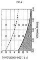
- the inventors of the present invention prepared 12 types in total of crystal samples with a predetermined nitrogen concentration of 3.9 x 10 13 number/cm 3 (calculated value for a shoulder position of crystal) and oxygen concentration of 13-15 ppma (JEIDA: Japan Electronic Industry Development Association standard), and two kinds of V/G during crystal growth of 0.27 and 0.325 [mm 2 /Kmin] and 6 kinds of passage time for the agglomeration temperature zone, 5, 13, 20, 30, 40 and 60 [min], which were selected for a temperature range of 1050°C to 1000°C since this temperature range corresponded to the agglomeration temperature zone of crystals doped with nitrogen at a nitrogen concentration of 10 13 order, and investigated the relationship between grown-in defect and thermal history.
- the plots represented with ⁇ indicate those satisfying the criterion of 10 number/6" wafer or less
- the plots represented with ⁇ indicate those not satisfying the criterion of 10 number/6" wafer or less.
- a nitrogen-doped silicon single crystal is produced by using pulling conditions falling into the hatched region shown in Fig. 1, a silicon wafer produced from the single crystal becomes a wafer containing extremely few defects at a level that has never been existed so far at least after annealing at 1200°C for 1 hour or more or 1150°C for 2 hours or more.
- C-mode good chip yield for TZDB (Time Zero Dielectric Breakdown) characteristic (dielectric breakdown electric field was 8 MV/cm or higher), which is an oxide dielectric breakdown voltage characteristic, should be 95% or more for a surface obtained by polishing for a depth of 3 ⁇ m from a surface after a heat treatment at 1200°C for 1 hour as the acceptability determination criterion
- the acceptability determination criterion was moderated and therefore the boundary shifts upward, i.e., it is represented by the broken line shown in Fig. 1.
- Fig. 3 Comparison of the grown-in defect densities of a wafer of the present invention containing extremely few defects and other conventional low defect crystals is shown in Fig. 3. As clearly seen from these results, it was found that the wafer of the present invention using the optimal nitrogen doped CZ wafer + argon annealing can be obtained as a wafer containing defects extremely fewer than those of any conventional low defect wafers depending on the production conditions therefor.
- parameters that determine the size and density of grown-in defects were investigated first.
- the parameters that determine the size and density of grown-in defects include nitrogen concentration, oxygen concentration, and ratio V/G of pulling rate V and temperature gradient G at a solid-liquid interface, and passage time PT for a temperature zone where defects agglomerate as thermal history during pulling of crystal.
- the oxygen concentration is usually fixed in many cases according to users' specifications. Further, this is a parameter directly relating to the BMD density, and a higher oxygen concentration can provide a higher BMD density but increases the size of grown-in defects. Therefore, it is preferably fixed within a moderate range (for example, 12-18 [ppma], in particular, 13-15 [ppma]).
- a higher nitrogen concentration is more desirable, because the aforementioned agglomeration inhibition effect and oxygen precipitation promotion effect are increased.
- it may also enlarge the OSF ring region, on which secondary defects such as dislocation loops may further be generated, and may change resistivity due to generation of N-O donors by binding with oxygen. Thus, it cannot be made higher so much either. Therefore, it is also desirable to fix it within a certain range (for example, about 1 to 20 x 10 13 [number/cm 3 ]), and not to use it for control of grown-in defects.
- the amount of generated N-O donors can be estimated from a difference in resistivity of a nitrogen-doped wafer measured before and after a heat treatment at about 500-800°C for generating N-O donors.
- the nitrogen concentration and oxygen concentration in a silicon single crystal are preferably adjusted to levels providing a desired BMD density within such ranges that the aforementioned problems should not be caused.
- the oxygen concentration can be selected to be within the range of 12-18 ppma, and the nitrogen concentration can be selected to be within the range of 1 x 10 13 to 2 x 10 14 [number/cm 3 ].
- V/G is a parameter that influences the concentration of point defects before the agglomeration of grown-in defects.
- silicon wafers are first produced from each of silicon single crystals produced with different V/G or PT, or silicon single crystals produced with different V/G and PT. While these silicon single crystals pulled with different conditions may be pulled by changing the conditions of V/G and PT for every batch of pulling of silicon ingot, the change of PT condition may be obtained within a single ingot by changing the pulling rate during pulling of the ingot.
- V/G is determined by the initial pulling rate, and a portion corresponding to a certain PT, which is determined by a pulling rate of later stage, can be prepared as a certain portion of the crystal.
- G required for calculation of V/G and PT are usually calculated by using results of thermal analysis (simulation), it is preferable for such a case to use results of transient analysis taking specific heat of crystal into consideration. If PT is calculated based on steady-state analysis that does not take the specific heat into consideration, a gap may be generated for different diameters of crystals. Therefore, when results of steady-state analysis are used, it is preferable to perform an experiment for every diameter taking influence of specific heat into consideration and perform calibration based on its results.
- G required for calculating V/G, it is preferable to use a value of G at a position as near the solid-liquid interface as possible for the calculation.
- an average for the range of from the melting point of silicon to 1400°C is used.
- the silicon single crystal pulling operation was simulated by using FEMAG (global heat transfer analysis software, F. Dupret, P. Nicodeme, Y. Ryckmans, P. Wouters and M.J. Crochet, Int. J. Heat Mass Transfer, 33, 1849 (1990)) in its quasi steady-state mode to calculate G.
- annealing conditions may be suitably selected as required. For example, it may be annealing at 1200°C for 1 hour, which is performed for hydrogen annealed wafers etc. as a standard treatment, annealing at 1150°C for 2 hours considering use of lower temperature in future and so forth.
- the annealing atmosphere can also be optionally selected from hydrogen, argon, mixed gas atmosphere thereof and so forth.
- a characteristic value of the wafers after the annealing is measured, their acceptability was determined by using a predetermined characteristic value as a standard, and correlation between the determined acceptability and V/G and PT.
- an evaluation apparatus that enables evaluation of defects along the depth direction for example, MO-601 (produced by Mitsui Mining and Smelting Co., Ltd.)
- MO-601 produced by Mitsui Mining and Smelting Co., Ltd.
- this apparatus enables evaluation of defects along the depth direction for a depth of about 5 ⁇ m. Therefore, if a defect-free layer of about 5 ⁇ m is desired, the evaluation can be performed by using this evaluation apparatus.
- the wafers after the annealing can be polished for a depth of desired defect-free layer and then measurement can be performed.
- a good chip yield for oxide dielectric breakdown voltage such as TZDB and TDDB (Time Dependent Dielectric Breakdown) can also be used as a parameter.
- the acceptability determination of the characteristic value of wafers can be performed on the basis of an arbitrary value, and correlation between the acceptability determination and V/G and PT can be obtained based on the value.
- Fig. 1 shows correlation of V/G and PT and grown-in defect density, where a grown-in defect density (LSTD density) of 10 number/6" wafer or less was used as a criterion for the acceptability determination. If a nitrogen-doped silicon single crystal is pulled with the conditions of V/G and PT selected from the hatched region shown in the correlation diagram, and a silicon wafer is produced from that single crystal and subjected to a predetermined heat treatment, a wafer having desired extremely few defects represented by a LSTD density of 10 number/6" or less will be obtained.
- LSTD density grown-in defect density
- a nitrogen-doped silicon single crystal. When a nitrogen-doped silicon single crystal. is pulled with V/G selected from the hatched region, it is preferably pulled so that at least the center portion of the crystal should become a V-rich region. This is because it becomes difficult to eliminate defects such as dislocation clusters existing in an I-rich region by a heat treatment, when an I-rich region is intermingled in a plane of the wafer produced from the pulled crystal.
- the pulling rate is first determined to be an arbitrary level, and then HZ can be analyzed and designed so that V/G and the passage time for agglomeration temperature zone should be within the predetermined ranges. For example, if the pulling rate is determined to be 1.0 [mm/min] and G is determined to be 3.5 [K/mm], V/G is calculated to be 0.286 [mm 2 /Kmin].
- the region of 1050-1000°C is designed to be a length of 3 cm or less so that the passage time for the agglomeration temperature zone should be at least 30 minutes or less (about 35 minutes is considered to be allowable in an actual operation), the above intended design should be satisfied.
- HZ-A When such an HZ (referred to as HZ-A) was actually produced, a crystal was grown with a pulling rate, oxygen concentration and nitrogen concentration adjusted to be 1.0 [mm/min], about 14 [ppma] and 5 x 10 13 [number/cm 3 ], respectively, and a silicon wafer was produced and subjected to argon annealing at 1200°C for 1 hour, a crystal free from COPs having a size of 0.09 ⁇ m or more at a position of a depth of 3 ⁇ m from the wafer surface could be obtained.
- the change corresponds to use of a higher oxygen concentration (for example, a case where more BMDs are desired) or a lower nitrogen concentration (for example, a case where defects unique to nitrogen may constitute a disturbance)
- care must be paid, and the boundary line shift toward the disadvantageous direction. Therefore, in such a case, it is desirable to newly obtain a boundary line for a silicon single crystal in the disadvantageous side of the boundary line through a similar experiment by producing a crystal with changing V/G and PT.
- the kinds of samples may be fewer.
- silicon single crystals of a diameter of 6 inches, p-type, resistivity of 10 ⁇ cm and crystal orientation of ⁇ 100> were pulled with changing V/G and the agglomeration temperature zone passage time PT, and processed into mirror-polished wafers in a conventional manner.
- V/G was adjusted to be 0.27 and 0.325 [mm 2 /Kmin] (G for V/G was calculated by performing simulation in the quasi steady-state mode of the aforementioned FEMAG), and the passage time for the agglomeration temperature zone (1050-1000°C) was adjusted at six kinds of levels, 5, 13, 20, 30, 40 and 60 [min].
- silicon single crystals were produced with changing PT by a method of changing the pulling rate V during the pulling, and the nitrogen concentration was controlled to be 3.9 x 10 13 [number/cm 3 ] (calculated value at a shoulder position of crystals) and the oxygen concentration was controlled to be 13-15 ppma (JEIDA).
- the crystals were first pulled at a pulling rate V1 (1.0 or 1.2 mm/min) for a length of 50 cm of the body from the crystal shoulder, then the pulling rate was rapidly changed from V1 to V2 (pulling rate selected from the range of 1.8-0.3 mm/min) during the pulling for the length of 50 cm to 51 cm, so that the diameter should not be changed as much as possible, and then the crystals were pulled at V2 for a length of 51 cm or more.
- V1 1.0 or 1.2 mm/min
- V2 pulling rate selected from the range of 1.8-0.3 mm/min
- V/G is determined by V1 and PT is determined by V2 for a position within a length of 37-50 cm of the crystal body during the pulling. Therefore, if a plurality of crystals are pulled with conditions in which V2 is varied, there can be obtained crystals' for which V/G is constant but PT is different.
- the position at a length of 37 cm of the body referred to herein means a position at which the temperature of the crystal is 1050°C (upper limit of the agglomeration temperature zone) when the crystal is pulled for 50 cm.
- an OSF ring is generated for the length of about 48 cm to 50 cm due to the rapid change of the pulling rate, a portion of the lengths of about 37-45 cm must be used in order to eliminate the influence of the OSF ring.
- COPs of the obtained wafers in the as-grown state were measured (measurement apparatus: SP-1 produced by KLA Tencor Co., measurable COP size: 0.09 ⁇ m or more).
- SP-1 produced by KLA Tencor Co.
- measurable COP size 0.09 ⁇ m or more.
- COPs showed clear correlation with respect to the thermal history, and a higher V/G value and a longer agglomeration temperature zone passage time PT provided a larger size and a larger density (Fig. 4, Fig. 5).
- COPs were well eliminated in samples undergone the annealing of 1200°C/1 h and obtained with V/G of 0.27 [mm 2 /Kmin] and a passage time PT of 40 minutes or less, or V/G of 0.325 [mm 2 /Kmin] and a passage time PT of 30 minutes or less, while COPs were considerably eliminated in samples undergone the annealing of 1150°C/2 h obtained with V/G of 0.27 [mm 2 /Kmin] and a passage time PT of 20 minutes or less, or V/G of 0.325 [mm 2 /Kmin] and a passage time PT of 13 minutes or less.
- a COP level of 70 number/wafer after the remeasurement was used as a criterion for the acceptability determination to prepare graphs representing the correlation with respect to V/G and PT.
- the graph for silicon wafers undergone the heat treatment of 1150°C/2 h was shown in Fig. 1 (solid line), and the graph for silicon wafers undergone the heat treatment of 1200°C/1 h was shown in Fig. 2, respectively. From these graphs, it can be seen that, if a silicon single crystal is pulled under a condition indicated by a position below each of the boundary lines of Figs. 1 and 2 and a wafer is produced from the crystal and subjected to each of the heat treatments, a wafer in which a region for a depth of 3 ⁇ m is substantially free from voids can be obtained.
- An oxide film was formed on a surface of a silicon wafer produced under the same conditions as in Example 1 (wafer undergone the heat treatment and polishing for a depth of 3 ⁇ m), and oxide dielectric breakdown voltages (TZDB, TDDB) of the wafer were measured under the following conditions. Then, graphs representing correlation with V/G and PT were prepared with a criterion for the acceptability determination that 95% of C-mode good chip yield for TZDB (dielectric breakdown electric field: 8 MV/cm or more) and 95% of ⁇ -mode good chip yield (charge amount at the time of dielectric breakdown was 25 C/cm 2 or more) were both satisfied.
- the measurement conditions for TZDB and TDDB are shown below.
- Oxide film thickness (25.5 [nm]), gate area (8 [mm 2 ]), current in decision (1 [mA]), measurement number (100 [dot/wafer]).
- Oxide film thickness (25.5 [nm]), gate area (4 [mm 2 ]), stress current density (0.01 [A/cm2]), measurement number (100 [dot/wafer]), measurement temperature (100°C).
- a nitrogen-doped crystal can be produced with conditions represented by a position below the boundary line shown in Fig. 2. If the production conditions are determined as described above, nitrogen-doped annealed wafers with stable quality can be obtained.
- Silicon single crystals of p-type, resistivity of 10 ⁇ cm and crystal orientation of ⁇ 100> were pulled with conditions of V/G of 0.27 [mm 2 /Kmin] (G for V/G was calculated by performing simulation in the quasi steady-state mode of the aforementioned FEMAG), and a passage time PT for the agglomeration temperature zone (1050-1000°C) of 13 [min] as conditions indicated by a position below the boundary line (solid line) in Fig. 1, and processed into mirror-polished wafers.
- the nitrogen concentration was controlled to be 3.9 x 10 13 [number/cm 3 ] (calculated value at a shoulder position of crystals) and the oxygen concentration was controlled to be 13-15 ppma (JEIDA).
- LSTDs grown-in defects
- the aforementioned embodiments were explained for cases where silicon single crystals having a diameter of 6 inches were grown.
- the present invention is not limited to them, and can also be applied to silicon single crystals having a diameter of 8-16 inches or larger.
- the present invention can of course be used for the so-called MCZ method in which a horizontal magnetic field, vertical magnetic field, cusp magnetic field or the like is applied to silicon melt.
Landscapes
- Chemical & Material Sciences (AREA)
- Engineering & Computer Science (AREA)
- Crystallography & Structural Chemistry (AREA)
- Materials Engineering (AREA)
- Metallurgy (AREA)
- Organic Chemistry (AREA)
- General Physics & Mathematics (AREA)
- Physics & Mathematics (AREA)
- Computer Hardware Design (AREA)
- Manufacturing & Machinery (AREA)
- Condensed Matter Physics & Semiconductors (AREA)
- Microelectronics & Electronic Packaging (AREA)
- Power Engineering (AREA)
- Health & Medical Sciences (AREA)
- Life Sciences & Earth Sciences (AREA)
- Food Science & Technology (AREA)
- Medicinal Chemistry (AREA)
- Analytical Chemistry (AREA)
- Biochemistry (AREA)
- General Health & Medical Sciences (AREA)
- Immunology (AREA)
- Pathology (AREA)
- Crystals, And After-Treatments Of Crystals (AREA)
Applications Claiming Priority (3)
| Application Number | Priority Date | Filing Date | Title |
|---|---|---|---|
| JP2000015537 | 2000-01-25 | ||
| JP2000015537 | 2000-01-25 | ||
| PCT/JP2001/000302 WO2001055485A1 (fr) | 2000-01-25 | 2001-01-18 | Plaquette de silicium, procede de determination de la condition dans laquelle est produit un monocristal de silicium et procede de production d'une plaquette de silicium |
Publications (3)
| Publication Number | Publication Date |
|---|---|
| EP1195455A1 true EP1195455A1 (fr) | 2002-04-10 |
| EP1195455A4 EP1195455A4 (fr) | 2008-02-13 |
| EP1195455B1 EP1195455B1 (fr) | 2011-04-13 |
Family
ID=18542817
Family Applications (1)
| Application Number | Title | Priority Date | Filing Date |
|---|---|---|---|
| EP01901424A Expired - Lifetime EP1195455B1 (fr) | 2000-01-25 | 2001-01-18 | Procede de determination de la condition dans laquelle est produit un monocristal de silicium et procede de production d'une plaquette de silicium |
Country Status (7)
| Country | Link |
|---|---|
| US (1) | US6599360B2 (fr) |
| EP (1) | EP1195455B1 (fr) |
| JP (1) | JP3565205B2 (fr) |
| KR (1) | KR100781728B1 (fr) |
| DE (1) | DE60144416D1 (fr) |
| TW (1) | TW512465B (fr) |
| WO (1) | WO2001055485A1 (fr) |
Cited By (4)
| Publication number | Priority date | Publication date | Assignee | Title |
|---|---|---|---|---|
| EP1275755A1 (fr) * | 2000-03-29 | 2003-01-15 | Shin-Etsu Handotai Co., Ltd | Plaquette de silicium et procede de production d'un monocristal de silicium |
| EP1536044A1 (fr) * | 2002-07-12 | 2005-06-01 | Shin-Etsu Handotai Co., Ltd | Tranche de silicium pour croissance epitaxiale, tranche epitaxiale, et procede de fabrication correspondant |
| US6902618B2 (en) | 2001-06-15 | 2005-06-07 | Shin-Etsu Handotai Co., Ltd. | Silicon single crystal wafer having void denuded zone on the surface and diameter of above 300 mm and its production method |
| US7875116B2 (en) | 2005-03-28 | 2011-01-25 | Sumco Techxiv Corporation | Silicon single crystal producing method, annealed wafer, and method of producing annealed wafer |
Families Citing this family (20)
| Publication number | Priority date | Publication date | Assignee | Title |
|---|---|---|---|---|
| US7084459B2 (en) * | 2001-05-29 | 2006-08-01 | Nippon Steel Corporation | SOI substrate |
| JP2003059932A (ja) | 2001-08-08 | 2003-02-28 | Toshiba Ceramics Co Ltd | シリコン単結晶ウエハの製造方法およびシリコン単結晶ウエハ |
| EP1456875A2 (fr) * | 2001-12-21 | 2004-09-15 | MEMC Electronic Materials, Inc. | Tranches de silicium a precipitation ideale de l'oxygene avec des centres de nucleation de precipitat d'oxygene stabilise d'azote/carbone et procede de fabrication correspondant |
| CN100472001C (zh) * | 2003-02-25 | 2009-03-25 | 株式会社上睦可 | 硅晶片、soi衬底、硅单晶生长方法,硅晶片制造方法及soi衬底制造方法 |
| KR100573473B1 (ko) * | 2004-05-10 | 2006-04-24 | 주식회사 실트론 | 실리콘 웨이퍼 및 그 제조방법 |
| JP2006054350A (ja) * | 2004-08-12 | 2006-02-23 | Komatsu Electronic Metals Co Ltd | 窒素ドープシリコンウェーハとその製造方法 |
| KR100693917B1 (ko) * | 2004-12-31 | 2007-03-12 | 주식회사 실트론 | 실리콘 단결정 |
| JP4604889B2 (ja) * | 2005-05-25 | 2011-01-05 | 株式会社Sumco | シリコンウェーハの製造方法、並びにシリコン単結晶育成方法 |
| DE102005028202B4 (de) * | 2005-06-17 | 2010-04-15 | Siltronic Ag | Verfahren zur Herstellung von Halbleiterscheiben aus Silizium |
| JP5121139B2 (ja) * | 2005-12-27 | 2013-01-16 | ジルトロニック アクチエンゲゼルシャフト | アニールウエハの製造方法 |
| JP4805681B2 (ja) * | 2006-01-12 | 2011-11-02 | ジルトロニック アクチエンゲゼルシャフト | エピタキシャルウェーハおよびエピタキシャルウェーハの製造方法 |
| US20090206275A1 (en) * | 2007-10-03 | 2009-08-20 | Silcon Genesis Corporation | Accelerator particle beam apparatus and method for low contaminate processing |
| JP4862857B2 (ja) * | 2008-05-02 | 2012-01-25 | 信越半導体株式会社 | シリコン単結晶ウェーハ評価用の標準サンプル、その製造方法及び標準サンプルを用いた評価方法 |
| JP5346744B2 (ja) * | 2008-12-26 | 2013-11-20 | ジルトロニック アクチエンゲゼルシャフト | シリコンウエハ及びその製造方法 |
| JP5678846B2 (ja) * | 2011-09-08 | 2015-03-04 | 信越半導体株式会社 | シリコン単結晶中窒素濃度算出方法および抵抗シフト量算出方法 |
| FR3055563B1 (fr) * | 2016-09-08 | 2018-09-14 | Commissariat A L'energie Atomique Et Aux Energies Alternatives | Procede de tri de plaquettes en silicium en fonction de leur duree de vie volumique |
| JP6971622B2 (ja) * | 2017-05-10 | 2021-11-24 | グローバルウェーハズ・ジャパン株式会社 | 半導体ウェハの製造方法及び半導体ウェハ |
| JP7247879B2 (ja) * | 2019-12-20 | 2023-03-29 | 株式会社Sumco | 単結晶シリコンウェーハの酸化膜耐圧の評価方法 |
| JP2022129531A (ja) * | 2021-02-25 | 2022-09-06 | グローバルウェーハズ・ジャパン株式会社 | シリコンウェーハの製造方法およびシリコンウェーハ |
| CN113897671B (zh) * | 2021-09-30 | 2023-05-05 | 西安奕斯伟材料科技股份有限公司 | 一种氮掺杂单晶硅棒的制备方法 |
Citations (5)
| Publication number | Priority date | Publication date | Assignee | Title |
|---|---|---|---|---|
| JPH10208987A (ja) * | 1997-01-27 | 1998-08-07 | Komatsu Electron Metals Co Ltd | 水素熱処理用シリコンウェーハ及びその製造方法 |
| JPH11157996A (ja) * | 1997-11-21 | 1999-06-15 | Shin Etsu Handotai Co Ltd | 結晶欠陥の少ないシリコン単結晶の製造方法及びシリコン単結晶ウエーハ |
| US5954873A (en) * | 1995-05-31 | 1999-09-21 | Sumitomo Sitix Corporation | Manufacturing method for a silicon single crystal wafer |
| EP0964082A1 (fr) * | 1998-06-11 | 1999-12-15 | Shin-Etsu Handotai Company Limited | Plaquette de silicium monocristallin et procédé pour sa production |
| EP1074643A1 (fr) * | 1998-11-19 | 2001-02-07 | Shin-Etsu Handotai Co., Ltd | Plaquette de silicium monocristallin presentant peu de defauts cristallins et procede de fabrication correspondant |
Family Cites Families (5)
| Publication number | Priority date | Publication date | Assignee | Title |
|---|---|---|---|---|
| JPH06103714B2 (ja) | 1990-11-22 | 1994-12-14 | 信越半導体株式会社 | シリコン単結晶の電気特性検査方法 |
| JP3955674B2 (ja) * | 1998-03-19 | 2007-08-08 | 株式会社東芝 | 半導体ウェーハの製造方法及び半導体装置の製造方法 |
| DE19823962A1 (de) * | 1998-05-28 | 1999-12-02 | Wacker Siltronic Halbleitermat | Verfahren zur Herstellung eines Einkristalls |
| WO2001016410A1 (fr) | 1999-08-30 | 2001-03-08 | Shin-Etsu Handotai Co., Ltd. | Procede de fabrication de silicium monocristallin, silicium monocristallin fabrique par ce procede et plaquette de silicium |
| JP5625533B2 (ja) * | 2010-06-22 | 2014-11-19 | トヨタ自動車株式会社 | 内燃機関の制御装置 |
-
2001
- 2001-01-18 US US09/936,920 patent/US6599360B2/en not_active Expired - Lifetime
- 2001-01-18 EP EP01901424A patent/EP1195455B1/fr not_active Expired - Lifetime
- 2001-01-18 JP JP2001554510A patent/JP3565205B2/ja not_active Expired - Fee Related
- 2001-01-18 KR KR1020017012237A patent/KR100781728B1/ko active IP Right Grant
- 2001-01-18 WO PCT/JP2001/000302 patent/WO2001055485A1/fr active Application Filing
- 2001-01-18 DE DE60144416T patent/DE60144416D1/de not_active Expired - Lifetime
- 2001-01-20 TW TW090101539A patent/TW512465B/zh not_active IP Right Cessation
Patent Citations (5)
| Publication number | Priority date | Publication date | Assignee | Title |
|---|---|---|---|---|
| US5954873A (en) * | 1995-05-31 | 1999-09-21 | Sumitomo Sitix Corporation | Manufacturing method for a silicon single crystal wafer |
| JPH10208987A (ja) * | 1997-01-27 | 1998-08-07 | Komatsu Electron Metals Co Ltd | 水素熱処理用シリコンウェーハ及びその製造方法 |
| JPH11157996A (ja) * | 1997-11-21 | 1999-06-15 | Shin Etsu Handotai Co Ltd | 結晶欠陥の少ないシリコン単結晶の製造方法及びシリコン単結晶ウエーハ |
| EP0964082A1 (fr) * | 1998-06-11 | 1999-12-15 | Shin-Etsu Handotai Company Limited | Plaquette de silicium monocristallin et procédé pour sa production |
| EP1074643A1 (fr) * | 1998-11-19 | 2001-02-07 | Shin-Etsu Handotai Co., Ltd | Plaquette de silicium monocristallin presentant peu de defauts cristallins et procede de fabrication correspondant |
Non-Patent Citations (3)
| Title |
|---|
| IIDA M ET AL: "EFFECTS OF LIGHT ELEMENT IMPURITIES ON THE FORMATION OF GROWN-IN DEFECTS FREE REGION OF CZOCHRALSKI SILICON SINGLE CRYSTAL" ELECTROCHEMICAL SOCIETY PROCEEDINGS, ELECTROCHEMICAL SOCIETY, PENNINGTON, NJ, US, vol. 99-1, May 1999 (1999-05), pages 499-510, XP002936579 ISSN: 0161-6374 * |
| NAKAMURA K ET AL: "Formation process of grown-in defects in Czochralski grown silicon crystals" JOURNAL OF CRYSTAL GROWTH, ELSEVIER, AMSTERDAM, NL, vol. 180, no. 1, 1 September 1997 (1997-09-01), pages 61-72, XP004087579 ISSN: 0022-0248 * |
| See also references of WO0155485A1 * |
Cited By (6)
| Publication number | Priority date | Publication date | Assignee | Title |
|---|---|---|---|---|
| EP1275755A1 (fr) * | 2000-03-29 | 2003-01-15 | Shin-Etsu Handotai Co., Ltd | Plaquette de silicium et procede de production d'un monocristal de silicium |
| EP1275755A4 (fr) * | 2000-03-29 | 2008-02-27 | Shinetsu Handotai Kk | Plaquette de silicium et procede de production d'un monocristal de silicium |
| US6902618B2 (en) | 2001-06-15 | 2005-06-07 | Shin-Etsu Handotai Co., Ltd. | Silicon single crystal wafer having void denuded zone on the surface and diameter of above 300 mm and its production method |
| EP1536044A1 (fr) * | 2002-07-12 | 2005-06-01 | Shin-Etsu Handotai Co., Ltd | Tranche de silicium pour croissance epitaxiale, tranche epitaxiale, et procede de fabrication correspondant |
| EP1536044A4 (fr) * | 2002-07-12 | 2009-05-13 | Shinetsu Handotai Kk | Tranche de silicium pour croissance epitaxiale, tranche epitaxiale, et procede de fabrication correspondant |
| US7875116B2 (en) | 2005-03-28 | 2011-01-25 | Sumco Techxiv Corporation | Silicon single crystal producing method, annealed wafer, and method of producing annealed wafer |
Also Published As
| Publication number | Publication date |
|---|---|
| DE60144416D1 (de) | 2011-05-26 |
| EP1195455A4 (fr) | 2008-02-13 |
| KR20010105392A (ko) | 2001-11-28 |
| JP3565205B2 (ja) | 2004-09-15 |
| KR100781728B1 (ko) | 2007-12-03 |
| US20030015131A1 (en) | 2003-01-23 |
| WO2001055485A1 (fr) | 2001-08-02 |
| TW512465B (en) | 2002-12-01 |
| US6599360B2 (en) | 2003-07-29 |
| EP1195455B1 (fr) | 2011-04-13 |
Similar Documents
| Publication | Publication Date | Title |
|---|---|---|
| US6599360B2 (en) | Silicon wafer, method for determining production conditions of silicon single crystal and method for producing silicon wafer | |
| US7404856B2 (en) | Nitrogen-doped silicon substantially free of oxidation induced stacking faults | |
| US6663708B1 (en) | Silicon wafer, and manufacturing method and heat treatment method of the same | |
| US6743289B2 (en) | Thermal annealing process for producing low defect density single crystal silicon | |
| EP1926134A1 (fr) | Procédé de fabrication de tranches de silicium épitaxiale | |
| JP4699675B2 (ja) | アニールウェーハの製造方法 | |
| EP1502972B1 (fr) | Plaquette a cristal unique de silicium, plaque epitaxiale, ainsi que procede permettant de produire un cristal unique de silicium | |
| EP1154048B1 (fr) | Procede de fabrication d'une tranche de silicium epitaxiee | |
| US6902618B2 (en) | Silicon single crystal wafer having void denuded zone on the surface and diameter of above 300 mm and its production method | |
| EP1074643A1 (fr) | Plaquette de silicium monocristallin presentant peu de defauts cristallins et procede de fabrication correspondant | |
| JP2002016071A (ja) | シリコンウェーハの製造方法及びその方法により製造されたシリコンウェーハ | |
| EP1127962B1 (fr) | Procede de fabrication de silicium monocristallin, silicium monocristallin fabrique par ce procede et plaquette de silicium | |
| JP2004282088A (ja) | シリコンウエーハ | |
| JP2001102385A (ja) | 点欠陥の凝集体が存在しないシリコンウェーハ | |
| KR100725673B1 (ko) | 실리콘 웨이퍼 | |
| EP1669478B1 (fr) | Silicium dopé à l'azote sensiblement exempt d'oxydation induite par des défauts d'empilement | |
| JP2002134513A (ja) | シリコンウェーハの熱処理方法 |
Legal Events
| Date | Code | Title | Description |
|---|---|---|---|
| PUAI | Public reference made under article 153(3) epc to a published international application that has entered the european phase |
Free format text: ORIGINAL CODE: 0009012 |
|
| 17P | Request for examination filed |
Effective date: 20011010 |
|
| AK | Designated contracting states |
Kind code of ref document: A1 Designated state(s): AT BE CH CY DE DK ES FI FR GB GR IE IT LI LU MC NL PT SE TR |
|
| RBV | Designated contracting states (corrected) |
Designated state(s): DE FR GB IT |
|
| A4 | Supplementary search report drawn up and despatched |
Effective date: 20080114 |
|
| RIC1 | Information provided on ipc code assigned before grant |
Ipc: G01N 27/04 20060101ALI20080108BHEP Ipc: C30B 29/06 20060101AFI20010806BHEP Ipc: C30B 15/20 20060101ALI20080108BHEP Ipc: G01N 21/956 20060101ALI20080108BHEP Ipc: H01L 21/322 20060101ALI20080108BHEP Ipc: H01L 21/324 20060101ALI20080108BHEP Ipc: H01L 21/66 20060101ALI20080108BHEP |
|
| 17Q | First examination report despatched |
Effective date: 20080902 |
|
| RAP1 | Party data changed (applicant data changed or rights of an application transferred) |
Owner name: SHIN-ETSU HANDOTAI CO., LTD. |
|
| GRAP | Despatch of communication of intention to grant a patent |
Free format text: ORIGINAL CODE: EPIDOSNIGR1 |
|
| RTI1 | Title (correction) |
Free format text: METHOD FOR DETERMINING CONDITION UNDER WHICH SILICON SINGLE CRYSTAL IS PRODUCED, AND METHOD FOR PRODUCING SILICON WAFER |
|
| GRAS | Grant fee paid |
Free format text: ORIGINAL CODE: EPIDOSNIGR3 |
|
| GRAA | (expected) grant |
Free format text: ORIGINAL CODE: 0009210 |
|
| AK | Designated contracting states |
Kind code of ref document: B1 Designated state(s): DE FR GB IT |
|
| REG | Reference to a national code |
Ref country code: GB Ref legal event code: FG4D |
|
| REF | Corresponds to: |
Ref document number: 60144416 Country of ref document: DE Date of ref document: 20110526 Kind code of ref document: P |
|
| REG | Reference to a national code |
Ref country code: DE Ref legal event code: R096 Ref document number: 60144416 Country of ref document: DE Effective date: 20110526 |
|
| PLBE | No opposition filed within time limit |
Free format text: ORIGINAL CODE: 0009261 |
|
| STAA | Information on the status of an ep patent application or granted ep patent |
Free format text: STATUS: NO OPPOSITION FILED WITHIN TIME LIMIT |
|
| 26N | No opposition filed |
Effective date: 20120116 |
|
| REG | Reference to a national code |
Ref country code: DE Ref legal event code: R097 Ref document number: 60144416 Country of ref document: DE Effective date: 20120116 |
|
| PG25 | Lapsed in a contracting state [announced via postgrant information from national office to epo] |
Ref country code: IT Free format text: LAPSE BECAUSE OF FAILURE TO SUBMIT A TRANSLATION OF THE DESCRIPTION OR TO PAY THE FEE WITHIN THE PRESCRIBED TIME-LIMIT Effective date: 20110413 |
|
| GBPC | Gb: european patent ceased through non-payment of renewal fee |
Effective date: 20120118 |
|
| REG | Reference to a national code |
Ref country code: FR Ref legal event code: ST Effective date: 20120928 |
|
| PG25 | Lapsed in a contracting state [announced via postgrant information from national office to epo] |
Ref country code: GB Free format text: LAPSE BECAUSE OF NON-PAYMENT OF DUE FEES Effective date: 20120118 |
|
| PG25 | Lapsed in a contracting state [announced via postgrant information from national office to epo] |
Ref country code: FR Free format text: LAPSE BECAUSE OF NON-PAYMENT OF DUE FEES Effective date: 20120131 |
|
| PGFP | Annual fee paid to national office [announced via postgrant information from national office to epo] |
Ref country code: DE Payment date: 20200107 Year of fee payment: 20 |
|
| REG | Reference to a national code |
Ref country code: DE Ref legal event code: R071 Ref document number: 60144416 Country of ref document: DE |