EP1193602A2 - Mémoire et limitation d'accès - Google Patents
Mémoire et limitation d'accès Download PDFInfo
- Publication number
- EP1193602A2 EP1193602A2 EP01308341A EP01308341A EP1193602A2 EP 1193602 A2 EP1193602 A2 EP 1193602A2 EP 01308341 A EP01308341 A EP 01308341A EP 01308341 A EP01308341 A EP 01308341A EP 1193602 A2 EP1193602 A2 EP 1193602A2
- Authority
- EP
- European Patent Office
- Prior art keywords
- data
- area
- memory
- memory apparatus
- written
- Prior art date
- Legal status (The legal status is an assumption and is not a legal conclusion. Google has not performed a legal analysis and makes no representation as to the accuracy of the status listed.)
- Withdrawn
Links
Images

Classifications
-
- G—PHYSICS
- G11—INFORMATION STORAGE
- G11C—STATIC STORES
- G11C17/00—Read-only memories programmable only once; Semi-permanent stores, e.g. manually-replaceable information cards
-
- G—PHYSICS
- G06—COMPUTING; CALCULATING OR COUNTING
- G06F—ELECTRIC DIGITAL DATA PROCESSING
- G06F21/00—Security arrangements for protecting computers, components thereof, programs or data against unauthorised activity
- G06F21/70—Protecting specific internal or peripheral components, in which the protection of a component leads to protection of the entire computer
- G06F21/78—Protecting specific internal or peripheral components, in which the protection of a component leads to protection of the entire computer to assure secure storage of data
- G06F21/79—Protecting specific internal or peripheral components, in which the protection of a component leads to protection of the entire computer to assure secure storage of data in semiconductor storage media, e.g. directly-addressable memories
-
- G—PHYSICS
- G06—COMPUTING; CALCULATING OR COUNTING
- G06F—ELECTRIC DIGITAL DATA PROCESSING
- G06F12/00—Accessing, addressing or allocating within memory systems or architectures
- G06F12/14—Protection against unauthorised use of memory or access to memory
- G06F12/1416—Protection against unauthorised use of memory or access to memory by checking the object accessibility, e.g. type of access defined by the memory independently of subject rights
- G06F12/1425—Protection against unauthorised use of memory or access to memory by checking the object accessibility, e.g. type of access defined by the memory independently of subject rights the protection being physical, e.g. cell, word, block
- G06F12/1433—Protection against unauthorised use of memory or access to memory by checking the object accessibility, e.g. type of access defined by the memory independently of subject rights the protection being physical, e.g. cell, word, block for a module or a part of a module
Definitions
- the present invention relates to a memory apparatus and a memory access restricting method that use a reversibly non-writable memory.
- a reversibly non-writable memory of which data can be written one time is known.
- OTP One Time Programmable ROM
- the related art reference is a non-volatile reversibly non-writable memory. In other words, according to the related art reference, once data is written, it cannot be erased. Thus, even if the power of the memory is turned off, written data is kept retained.
- the reversibly non-writable memory can be fabricated at a lower cost than the a flash memory.
- An embodiment of the present invention seeks to provide a memory apparatus and an access restricting method that allow a reversibly non-writable memory to be more widely used.
- a first aspect of the present invention is a memory apparatus composed of a reversibly non-writable memory, comprising an initial data area to which initial data is pre-written, a user data area to which data prepared by the user is written, and a setup data area to which a setup state is written, wherein when data that is different from the initial data is written to said initial data area, said user area becomes non-accessible, and wherein when the used state of the memory is in the setup state, said user data area becomes accessible.
- a second aspect of the present invention is a memory apparatus composed of a reversibly non-writable memory, comprising a first designated area to which initial data is pre-written, a user data area to which data prepared by the user is written, and a second designated area, wherein when predetermined data that is different from the initial data is written to said first designated area, said user data area becomes non-accessible, and wherein when data having a predetermined relation with predetermined data is written to said second designated area, said user data area becomes accessible.
- a third aspect of the present invention is an access restricting method for a non-volatile reversibly non-writable memory apparatus, when predetermined data is written to a first designated area of the memory apparatus, the predetermined area being access-restricted, comprising the steps of detecting whether or not the memory apparatus has become access-restricted, causing the memory apparatus to be changed to an access restricted state when the memory apparatus has not been access-restricted, and causing the memory apparatus to be changed to an access permitted state when the memory apparatus has been access-restricted and the used state of the memory apparatus is in a predetermined state.
- a fourth aspect of the present invention is an access restricting method for a non-volatile reversibly non-writable memory apparatus, when predetermined data is written to a first designated area, a predetermined area being access-restricted, comprising the steps of detecting whether or not the memory apparatus has been access-restricted, causing the memory apparatus to be changed to an access restricted state when the memory apparatus has not been access-restricted, and causing the memory apparatus to be changed to an access permitted state when the memory apparatus has been access-restricted and data written to a second designated area of the memory apparatus has a predetermined relation with the predetermined data.
- pre-written data when a memory is used a predetermined number of times or when data that has a predetermined relation with particular data is written to a predetermined area of the memory, pre-written data can be accessed.
- the data may provide the user with a reward.
- the data may be advertisement/commercial information.
- the data will contribute to promote the promotion of the use of the memory apparatus, resulting in reducing the cost thereof.
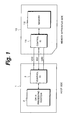
- Fig. 1 shows an outline of the structure of a system according to an embodiment of the present invention.
- a host side and a memory apparatus side are connected through a serial interface.
- a host side data processing device 1 has a data processing portion 2 and a control IC 3.
- a memory apparatus 10 has a control IC 11 and a memory 12.
- the memory apparatus 10 has a card-shaped structure attachable and detachable to/from the data processing device 1.
- the data processing portion 2 generates data written to the memory apparatus 10.
- the data processing portion 2 reads data from the memory apparatus 10 and performs various data processes for data that is read from the memory apparatus 10.
- the data processing device 1 is a digital electronic camera. A photographed picture is written to the memory apparatus 10. In addition, a picture is read from the memory apparatus 10.
- Another example of the data processing device 1 is an audio recording/reproducing device. Compressed audio data is written to the memory apparatus 10. In addition, compressed audio data is read from the memory apparatus 10.
- Each of the control ICs 3 an 11 comprises a parallel-serial converting circuit, a buffer memory (that temporarily stores data), and an interface circuit.
- a power line VCC, a data line DIO, and a ground line GND are disposed between the control ICs 3 and 11.
- a command and write data are transferred from the data processing device 1 to the memory apparatus 10 through the data line DIO.
- Read data is transferred from the memory apparatus 10 to the data processing device 1 through the data line DIO.
- signal lines for transferring a clock signal, a control signal, and so forth are disposed (not shown).
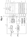
- Fig. 2 shows a detail of the structure of the memory apparatus 10 according to the embodiment.
- Data in a predetermined unit (for example, a horizontal stripe shaped area shown in Fig. 2) is read and written from/to the memory 12.
- Predetermined two areas of the memory 12 are boot areas 13a and 13b.
- Various types of information such as attribute information are pre-recorded to the boot areas 13a and 13b.
- attribute information For example, information that represents whether the memory apparatus is a read-only memory, an access restricted memory, or a rewritable memory is pre-recorded to the boot areas 13a and 13b.
- characteristics of the memory apparatuses are identified with the attribute information recorded in the boot areas 13a and 13b.
- the boot areas 13a and 13b are areas that are initially read by the data processing device 1 when the memory apparatus 10 is attached thereto.
- the boot areas 13a and 13b are areas that are always readable.
- the memory 12 has a designated area 14 and a hidden area (hatched area) 15.
- a memory area (user area) other than the boot areas 13a and 13b, the designated area 14, and the hidden area 15 is denoted by reference numeral 16.
- User data is written to the user area 16.
- the memory 12 that is a reversibly non-writable memory (OTP) is used from the beginning of the user area 16 (the highest area shown in Fig. 2).
- a setup value is written to an area 16a at the beginning of the user area 16.
- the setup value is a value representing the ratio of the total memory capacity and the used memory capacity of the memory 12.
- the setup value is represented in the write data unit of the memory 12.
- a setup value equivalent to the case that around 80 % of memory capacity is used is written to the area 16a.
- a flag (of for example one bit) that represents that the relevant area has been used is set. The record position of each flag is written to each area of the memory.
- hidden data is recorded to the hidden area 15.
- character data, music data, picture data, or a combination thereof as hidden data is recorded by a secondary memory provider for example a content provider or a content distributor.
- a private individual may record hidden data to the memory 12.
- hidden data is information that provides a reward to a user or advertisement/commercial information.
- An access controlling portion 21 is connected to the data line DIO of the control IC 11.
- the access controlling portion 21 controls the writing operation and reading operation for data to/from the memory 12.
- the access controlling portion 21 comprises a buffer memory (that stores data) and a register (that stores a command).
- a reset signal generating portion 23 is connected to the power line VCC.
- the reset signal generating portion 23 monitors the voltage fluctuation of the power line VCC, detects the power on state of the memory apparatus 10, and generates a reset signal corresponding to the detection of the power on state. Data written to the designated area 14 is loaded to the register 22 corresponding to the reset signal.
- the access controlling portion 21 is connected to the boot areas 13a and 13b and the user area 16 of the memory 12. Thus, the boot areas 13a and 13b and the user area 16 can be always accessed.
- a gate (switch) G0 is disposed between the access controlling portion 21 and the designated area 14 and the hidden area 15 of the memory 12. Once the gate G0 is turned off or on with a control signal, the current state is kept retained until the control signal is supplied.
- An initial state detecting portion 26 is disposed in the control IC 11.
- the initial state detecting portion 26 detects whether or not data that is read from the designated area 14 to the register 22 corresponding to the reset signal is in the initial state. With a detected output of the initial state detecting portion 26, the on/off state of the gate G0 is controlled.
- a used state detecting circuit 27 is disposed in the control IC 11.
- the setup value recorded in the area 16a and a flag that represents whether or not an area other than the area 16a has been used are supplied to the used state detecting circuit 27.
- the used state detecting circuit 27 detects whether or not the used memory capacity matches the setup value. With a detection signal that is generated corresponding to the detected result, the on/ff state of the gate G0 is controlled.
- the gate G0 When the detected result of the initial state detecting portion 26 represents that the data that has been read from the designated area 14 to the register 22 is in the initial state, the gate G0 is turned on. When the detected result represents that the data is not in the initial state, the gate G0 is turned off. When the detected result of the used state detecting circuit 27 represents that the used memory capacity does not match the setup value, the gate G0 is turned off. When the detected result of the used state detecting circuit 27 represents that the used memory capacity matches the setup value, the gate G0 is turned on. When the gate G0 is turned on, both the designated area 14 and the hidden area 15 can be accessed. With both the detection signal for the initial state and the detection signal of the used state detecting circuit 27, the gate G0 is controlled. In the control IC 11 shown in Fig. 2, a sequencer (controller) (not shown) composed of a CPU is disposed.
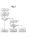
- Fig. 3 is a flow chart for explaining the operation of the sequencer of the control IC 11 according to the embodiment of the present invention.
- the reset signal generating portion 23 detects that the signal of the power line VCC goes high. As a result, the reset signal generating portion 23 generates the reset signal. With the reset signal, data recorded in the designated area 14 is loaded to the register 22 of the control IC 11 (at step S2).
- the initial state detecting portion 26 detects whether or not code loaded to the register 22 is the initial value.
- data recorded in the designated area 14 is the initial value.
- the initial value is a value that has been written before the memory apparatus 10 is shipped to the user.
- the initial value is code of which all bits are for example ones.
- the gate G0 is turned on.
- step S4 When the gate G0 is turned on, all areas of the memory 12 can be accessed (at step S4). In other words, in addition to the boot areas 13a and 13b and the user area 16 that are always accessible, data can be read from the designated area 14 and the hidden area 15. In addition, data can be written to a blank area.
- the user In the state that all areas are accessible, the user writes desired information to the hidden area 15. In addition, the user writes a desired setup value to the area 16a. Thereafter, the user records code that is different from the initial value to the area 16a. Thereafter, the user turns off the power of the memory 12. Since the memory 12 is a non-volatile memory, even if the power of the memory 12 is turned off, information written thereto is not erased. Thereafter, when the user turns on the power of the memory 12, data recorded in the designated area 14 is loaded to the register 22. In this state, since the loaded data is different from the initial value, the determined result at step S3 represents that the memory 12 is not in the initial state.
- the used state of the memory 12 is read to the used state detecting circuit 27.
- the setup value recorded in the area 16a is read to the used state detecting circuit 27.
- the used state detecting circuit 27 detects whether or not the used capacity of the memory 12 matches the setup value. For example, the used state detecting circuit 27 detects whether or not the used capacity of the memory 12 becomes 80 % of the setup value.
- the gate G0 When the used capacity does not match the setup value, the gate G0 is turned off. Thus, the designated area 14 and the hidden area 15 are non-accessible (at step S8).
- the gate G0 When the used capacity of the memory 12 matches the setup value recorded in the record area 16a, with the detection signal of the used state detecting circuit 27, the gate G0 is turned on. As a result, the designated area 14 and the hidden area 15 can be accessed (at step S7). In other words, hidden data recorded in the hidden area 15 can be read by the access controlling portion 21.
- the hidden area 15 can be accessed. Otherwise, hidden data recorded in the hidden area 15 cannot be accessed.
- the memory apparatus 10 allows hidden data to be used as win/fail mark or a point for a reward.
- the memory apparatus 10 can be used as an advertisement/commercial medium.
- the sponsor can circulate the memory 12 to a consumer at low cost or free of charge.
- the user can access a web site or apply for a reward.
- the number lots drawn may be increased corresponding to the acquired points.
- picture, music, number, or the like that is reproduced with hidden data may server as a password for accessing a secret Internet site.
- the sales of the memory apparatus can be promoted.
- the memory 12 is effective for private uses.
- Fig. 4 shows a detail of the structure of a memory apparatus 10 according to another embodiment (second embodiment) of the present invention.
- Boot areas 13a and 13b and a user area 16 can be always accessed by a data processing device 1.
- a second designated area 16b is formed in the user area 16.
- the designated area 1 represents a first designated area
- a designated area 2 represents a second designated area.
- a hidden area (hatched area) 15 is formed in a memory 12.
- Gates (switches) G1 and G2 are in parallel disposed between an access controlling portion 21 and the designated area 14 and the hidden area 15 of the memory 12. Once each of the gates G1 and G2 is turned on/off with a control signal, the state is kept retained until the next control signal is supplied.
- An initial state detecting portion 26 detects whether or not data that is read from the designated area 14 to a register 22 is in the initial state. With a detected output of the initial state detecting portion 26, the on/off state of the gate G2 is controlled. Data read to the register 22 is supplied to one input of a comparing circuit 24.
- a register 25 is disposed in a control IC 11.
- the register 25 stores data that is read from the second designated area 16b.
- An output of the register 25 is supplied to another input of the comparing circuit 24.
- the comparing circuit 24 compares outputs of the registers 22 and 25 and detects whether they match. With an output of the comparing circuit 24, the on/off state of the gate G1 is controlled.
- the gate G2 is controlled. In other words, when the data read to the register 22 is in the initial state, the gate G2 is turned on. When the data read to the register 22 is not in the initial state, the gate G2 is turned off.
- the comparing circuit 24 compares the data read from the designated area 14 to the register 22 with the data read from the second designated area 16b to the register 25. When the comparing circuit 24 has detected that they match, the gate G1 is turned on. When the gate G1 is turned on, both the designated area 14 and the hidden area 15 are accessible. In contrast, when the comparing circuit 24 has detected that they do not match, the gate G1 is turned off. Thus, both the designated area 14 and the hidden area 15 are non-accessible.
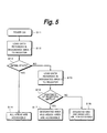
- Fig. 5 is a flow chart for explaining the operation of a sequencer of the control IC 11 according to the second embodiment of the present invention.
- a reset signal generating portion 23 detects that the signal level of a power line VCC goes high.
- the reset signal generating portion 23 generates a reset signal. With the reset signal, data recorded in the first designated area 14 of the memory 12 is loaded to the register 22 of the control IC 11 (at step S12).
- the initial state detecting portion 26 detects whether or not code loaded to the register 22 is the initial value.
- data recorded in the designated area 14 is the initial value.
- the initial value is a value that has been written to the designated area 14 before the memory apparatus 10 is delivered to the user.
- the gate G2 is turned on.
- step S14 When the gate G2 is turned on, all areas of the memory 12 can be accessed (at step S14). In other words, in addition to the boot areas 13a and 13b and the user area 16 that are always accessible, data can be read from the designated area 14 and the hidden area 15. In addition, data can be written to a blank area.
- the user In the state that all the areas are accessible, the user (for example, a secondary memory provider) writes desired information to the hidden area 15. Thereafter, the user records particular data that is different from the initial value to the first designated area 14. Thereafter, the user turns off the power of the memory apparatus 10. Since the memory 12 is a non-volatile memory, even if the power thereof is turned off, information written thereto is not erased. Thereafter, when the user turns on the power of the memory apparatus 10, data recorded in the designated area 14 is loaded to the register 22. In this case, since the loaded data (particular data) is different from the initial value, the determined result at step S13 represents that the data recorded in the register 22 is not the initial value.
- step S15 data recorded in the second designated area 16b of the memory 12 is loaded to the register 25.
- step S16 the comparing circuit 24 determines whether or not data recorded in the register 22 matches data recorded in the register 25. When they match, the designated area 14 and the hidden area 15 can be accessed (at step S17). Since the boot areas 13a and 13b and the user area 16 are always accessible, all the areas becomes accessible at step S17.
- the memory apparatus can be used for a stamp rally.
- a stamp rally For example, with a one-day train ticket, a one-week free ticket, an excursion ticket, or the like, the user may visit a predetermined number of designated places such as stations or play spots and write predetermined data (designated values) as with stamps obtained at such places to the second designated area 16b.
- predetermined data designated values
- data written to the second designated area 16b matches predetermined data written to the designated area 14.
- the gate G1 is turned on.
- the hidden area 15 can be accessed.
- data that is pre-written to the hidden area 15 may be a win mark, advertisement/commercial data, a point, or premium data.
- stamp data and date/time data an Internet web site that only users who finished the rally can access can be operated.
- a service using date/time data can be provided. Whenever each user finishes the rally, he or she may be able to apply for lottery. Alternatively, each user may apply for lottery any time in a predetermined period (drawing period).
- Places at which data is written to the second designated area 16b are not limited to stations and play spots.
- data may be written to the second designated area 16b.
- the memory apparatus is used for a digital camera of a particular maker, designated data is written to the designated area 16b.
- designated data is written to the designated area 16b.
- the memory apparatus is used for another device such as a note personal computer, designated data is written to the designated area 16b.
- a predetermined number of devices for example, five devices
- data written to the designated area 16b matches the predetermined data written in the designated area 14.
- the hidden area 15 can be accessed.
- the present invention is not limited to the above-described embodiments.
- the initial state when the power is turned on, the initial state is detected.
- the memory apparatus when the memory apparatus is attached, the initial state may be detected.
- the hidden area 15 can be accessed.
- a predetermined condition namely, there is a difference between the contents
- the hidden area 15 may be accessed.
- a storage medium such as a write once type optical disc may be used. In the case of the storage medium, an area on the innermost periphery side of the disc is equivalent to the boot area.
- a hidden area becomes accessible.
- data that matches predetermined data is written to a designated area, it becomes accessible.
- hidden data recorded in a hidden area a reword can be obtained. In this case, the sales of the memory apparatus can be promoted.
- new business models can be established.
Landscapes
- Engineering & Computer Science (AREA)
- Theoretical Computer Science (AREA)
- Computer Security & Cryptography (AREA)
- Physics & Mathematics (AREA)
- General Engineering & Computer Science (AREA)
- General Physics & Mathematics (AREA)
- Computer Hardware Design (AREA)
- Software Systems (AREA)
- Storage Device Security (AREA)
- Credit Cards Or The Like (AREA)
- Read Only Memory (AREA)
Applications Claiming Priority (2)
| Application Number | Priority Date | Filing Date | Title |
|---|---|---|---|
| JP2000300974 | 2000-09-29 | ||
| JP2000300974A JP4678084B2 (ja) | 2000-09-29 | 2000-09-29 | メモリ装置およびメモリアクセス制限方法 |
Publications (2)
| Publication Number | Publication Date |
|---|---|
| EP1193602A2 true EP1193602A2 (fr) | 2002-04-03 |
| EP1193602A3 EP1193602A3 (fr) | 2005-10-26 |
Family
ID=18782573
Family Applications (1)
| Application Number | Title | Priority Date | Filing Date |
|---|---|---|---|
| EP01308341A Withdrawn EP1193602A3 (fr) | 2000-09-29 | 2001-09-28 | Mémoire et limitation d'accès |
Country Status (7)
| Country | Link |
|---|---|
| US (1) | US6775754B2 (fr) |
| EP (1) | EP1193602A3 (fr) |
| JP (1) | JP4678084B2 (fr) |
| KR (1) | KR20020025799A (fr) |
| CN (1) | CN1270244C (fr) |
| MY (1) | MY127318A (fr) |
| TW (1) | TW521183B (fr) |
Cited By (2)
| Publication number | Priority date | Publication date | Assignee | Title |
|---|---|---|---|---|
| EP1855226A1 (fr) * | 2006-05-18 | 2007-11-14 | Phison Electronics Corp. | Système de securité de mémoire flash et méthode associée |
| US10387336B2 (en) | 2017-03-24 | 2019-08-20 | Micron Technology, Inc. | Memory protection based on system state |
Families Citing this family (21)
| Publication number | Priority date | Publication date | Assignee | Title |
|---|---|---|---|---|
| JP3979194B2 (ja) * | 2002-06-25 | 2007-09-19 | ソニー株式会社 | 情報記憶装置、およびメモリアクセス制御方法、並びにコンピュータ・プログラム |
| JP4016741B2 (ja) | 2002-06-25 | 2007-12-05 | ソニー株式会社 | 情報記憶装置、メモリアクセス制御システム、および方法、並びにコンピュータ・プログラム |
| JP3979195B2 (ja) * | 2002-06-25 | 2007-09-19 | ソニー株式会社 | 情報記憶装置、およびメモリアクセス制御方法、並びにコンピュータ・プログラム |
| US7296127B2 (en) | 2003-03-31 | 2007-11-13 | Intel Corporation | NoDMA cache |
| US7814554B1 (en) * | 2003-11-06 | 2010-10-12 | Gary Dean Ragner | Dynamic associative storage security for long-term memory storage devices |
| US7281102B1 (en) * | 2004-08-12 | 2007-10-09 | Vmware, Inc. | Restricting memory access to protect data when sharing a common address space |
| US7277999B1 (en) * | 2004-08-12 | 2007-10-02 | Vmware, Inc. | Restricting memory access to protect data when sharing a common address space |
| US7277998B1 (en) * | 2004-08-12 | 2007-10-02 | Vmware, Inc. | Restricting memory access to protect data when sharing a common address space |
| CN100358050C (zh) * | 2005-05-25 | 2007-12-26 | 深圳兆日技术有限公司 | 一种防止存储器攻击的隐藏rom的方法 |
| JP4911576B2 (ja) * | 2006-03-24 | 2012-04-04 | 株式会社メガチップス | 情報処理装置および追記型メモリ利用方法 |
| JP4577300B2 (ja) * | 2006-11-17 | 2010-11-10 | 日本電気株式会社 | ストレージ装置、ストレージ装置のアクセス制御方法、ストレージ装置のアクセス制御プログラム |
| JP5186808B2 (ja) * | 2007-05-29 | 2013-04-24 | 富士ゼロックス株式会社 | 情報処理装置及びプログラム |
| US8327059B2 (en) * | 2009-09-30 | 2012-12-04 | Vmware, Inc. | System and method to enhance memory protection for programs in a virtual machine environment |
| CN103813101B (zh) * | 2014-02-18 | 2019-03-08 | 青岛海信移动通信技术股份有限公司 | 一种终端中的相机启动方法及终端 |
| CN105989299A (zh) * | 2014-11-13 | 2016-10-05 | 株式会社东芝 | 存储装置的管理方法及计算机系统 |
| CN105988282A (zh) * | 2015-11-08 | 2016-10-05 | 乐视移动智能信息技术(北京)有限公司 | 相机模组故障检测方法及装置 |
| CN105573923A (zh) * | 2015-12-11 | 2016-05-11 | 中国航空工业集团公司西安航空计算技术研究所 | 一种访问多块存储空间的控制电路 |
| US10387333B2 (en) * | 2017-01-05 | 2019-08-20 | Qualcomm Incorporated | Non-volatile random access memory with gated security access |
| CN108922567B (zh) * | 2018-06-29 | 2020-08-21 | 北京同方光盘股份有限公司 | 光盘隐藏数据读取次数的限定的方法及装置 |
| US11468037B2 (en) | 2019-03-06 | 2022-10-11 | Semiconductor Components Industries, Llc | Memory device and data verification method |
| US11507282B2 (en) * | 2020-12-04 | 2022-11-22 | Winbond Electronics Corp. | Data processing system and method for reading instruction data of instruction from memory including a comparison stage for preventing execution of wrong instruction data |
Citations (5)
| Publication number | Priority date | Publication date | Assignee | Title |
|---|---|---|---|---|
| US4211919A (en) * | 1977-08-26 | 1980-07-08 | Compagnie Internationale Pour L'informatique | Portable data carrier including a microprocessor |
| US4864542A (en) * | 1987-03-16 | 1989-09-05 | Hitachi Maxell, Ltd. | Memory cartridge having stored data protecting function and memory protecting method |
| JPH1165936A (ja) * | 1997-06-12 | 1999-03-09 | Oki Micro Design Miyazaki:Kk | メモリ装置 |
| US6009012A (en) * | 1998-06-03 | 1999-12-28 | Motorola Inc. | Microcontroller having a non-volatile memory and a method for selecting an operational mode |
| JP2000076133A (ja) * | 1998-06-04 | 2000-03-14 | Texas Instr Inc <Ti> | 一度だけ書込み可能なメモリ内のプログラムデ―タのセキュリティ保証方法 |
Family Cites Families (14)
| Publication number | Priority date | Publication date | Assignee | Title |
|---|---|---|---|---|
| ATE65632T1 (de) * | 1985-07-08 | 1991-08-15 | Siemens Ag | Verfahren zum kontrollieren eines speicherzugriffs auf einer chipkarte und anordnung zur durchfuehrung des verfahrens. |
| JP2575358B2 (ja) * | 1986-03-28 | 1997-01-22 | シチズン時計株式会社 | Icカ−ド |
| US5282247A (en) * | 1992-11-12 | 1994-01-25 | Maxtor Corporation | Apparatus and method for providing data security in a computer system having removable memory |
| JPH0844628A (ja) * | 1994-08-03 | 1996-02-16 | Hitachi Ltd | 不揮発性メモリ、およびそれを用いたメモリカード、情報処理装置、ならびに不揮発性メモリのソフトウェアライトプロテクト制御方法 |
| JPH09223198A (ja) * | 1996-02-20 | 1997-08-26 | Dainippon Printing Co Ltd | 計数機能を有するicカード |
| JPH09253308A (ja) * | 1996-03-18 | 1997-09-30 | Sophia Co Ltd | 遊技情報媒体 |
| JPH09293022A (ja) * | 1996-04-24 | 1997-11-11 | Toshiba Corp | データ記録再生装置及び同装置におけるデータ保護方法 |
| JPH1049986A (ja) * | 1996-08-05 | 1998-02-20 | Sony Corp | 記録媒体、記録又は再生装置、記録又は再生方法 |
| JPH10228421A (ja) * | 1997-02-14 | 1998-08-25 | Nec Ic Microcomput Syst Ltd | メモリアクセス制御回路 |
| JPH11232884A (ja) * | 1998-02-09 | 1999-08-27 | Hitachi Ltd | 不揮発性メモリ装置 |
| JPH11249966A (ja) * | 1998-03-03 | 1999-09-17 | Nec Corp | 情報記憶装置 |
| US6915375B2 (en) * | 1998-08-31 | 2005-07-05 | Sony Corporation | Memory apparatus and a data-processing apparatus, and method for using the memory apparatus |
| DE19855596C2 (de) * | 1998-12-02 | 2002-10-24 | Orga Kartensysteme Gmbh | Tragbarer mikroprozessorgestützter Datenträger, der sowohl kontaktbehaftet als auch kontaktlos betreibbar ist |
| US6618789B1 (en) * | 1999-04-07 | 2003-09-09 | Sony Corporation | Security memory card compatible with secure and non-secure data processing systems |
-
2000
- 2000-09-29 JP JP2000300974A patent/JP4678084B2/ja not_active Expired - Fee Related
-
2001
- 2001-09-24 TW TW090123492A patent/TW521183B/zh not_active IP Right Cessation
- 2001-09-28 US US09/967,410 patent/US6775754B2/en not_active Expired - Fee Related
- 2001-09-28 MY MYPI20014556A patent/MY127318A/en unknown
- 2001-09-28 EP EP01308341A patent/EP1193602A3/fr not_active Withdrawn
- 2001-09-28 KR KR1020010060425A patent/KR20020025799A/ko not_active Application Discontinuation
- 2001-09-29 CN CNB011372532A patent/CN1270244C/zh not_active Expired - Fee Related
Patent Citations (5)
| Publication number | Priority date | Publication date | Assignee | Title |
|---|---|---|---|---|
| US4211919A (en) * | 1977-08-26 | 1980-07-08 | Compagnie Internationale Pour L'informatique | Portable data carrier including a microprocessor |
| US4864542A (en) * | 1987-03-16 | 1989-09-05 | Hitachi Maxell, Ltd. | Memory cartridge having stored data protecting function and memory protecting method |
| JPH1165936A (ja) * | 1997-06-12 | 1999-03-09 | Oki Micro Design Miyazaki:Kk | メモリ装置 |
| US6009012A (en) * | 1998-06-03 | 1999-12-28 | Motorola Inc. | Microcontroller having a non-volatile memory and a method for selecting an operational mode |
| JP2000076133A (ja) * | 1998-06-04 | 2000-03-14 | Texas Instr Inc <Ti> | 一度だけ書込み可能なメモリ内のプログラムデ―タのセキュリティ保証方法 |
Non-Patent Citations (2)
| Title |
|---|
| PATENT ABSTRACTS OF JAPAN vol. 1999, no. 08, 30 June 1999 (1999-06-30) & JP 11 065936 A (OKI MICRO DESIGN MIYAZAKI:KK; OKI ELECTRIC IND CO LTD), 9 March 1999 (1999-03-09) & US 6 230 244 B1 (KAI NOBUHIRO) 8 May 2001 (2001-05-08) * |
| PATENT ABSTRACTS OF JAPAN vol. 2000, no. 06, 22 September 2000 (2000-09-22) & JP 2000 076133 A (TEXAS INSTR INC <TI>), 14 March 2000 (2000-03-14) & US 6 160 734 A (HENDERSON ET AL) 12 December 2000 (2000-12-12) * |
Cited By (4)
| Publication number | Priority date | Publication date | Assignee | Title |
|---|---|---|---|---|
| EP1855226A1 (fr) * | 2006-05-18 | 2007-11-14 | Phison Electronics Corp. | Système de securité de mémoire flash et méthode associée |
| US10387336B2 (en) | 2017-03-24 | 2019-08-20 | Micron Technology, Inc. | Memory protection based on system state |
| US10838879B2 (en) | 2017-03-24 | 2020-11-17 | Micron Technology, Inc. | Memory protection based on system state |
| US11334502B2 (en) | 2017-03-24 | 2022-05-17 | Micron Technology, Inc. | Memory protection based on system state |
Also Published As
| Publication number | Publication date |
|---|---|
| TW521183B (en) | 2003-02-21 |
| US20020040423A1 (en) | 2002-04-04 |
| CN1270244C (zh) | 2006-08-16 |
| MY127318A (en) | 2006-11-30 |
| JP4678084B2 (ja) | 2011-04-27 |
| EP1193602A3 (fr) | 2005-10-26 |
| KR20020025799A (ko) | 2002-04-04 |
| US6775754B2 (en) | 2004-08-10 |
| CN1346093A (zh) | 2002-04-24 |
| JP2002108714A (ja) | 2002-04-12 |
Similar Documents
| Publication | Publication Date | Title |
|---|---|---|
| US6775754B2 (en) | Memory apparatus and memory access restricting method | |
| KR101157433B1 (ko) | 사용조건으로서 휴대 데이터 저장 디바이스의 사용자에게메시지의 전달 | |
| US20110238507A1 (en) | Combining user content with supplemental content at a data storage device | |
| US20070167720A1 (en) | Smart card control of medical devices | |
| TW594518B (en) | Digital contents selling method using communication network and system thereof | |
| KR960015528A (ko) | 메모리 카드와 그 기록, 재생 및 소거방법 | |
| US7061836B2 (en) | Method and apparatus for processing information data and management information thereof | |
| CN102112963B (zh) | 用于定制软件的方法和设备 | |
| US7167943B2 (en) | Memory apparatus | |
| US7860947B2 (en) | Storage medium and downloading method | |
| EP1193601A2 (fr) | Dispositif de mémoire et procédé de limitation d'accès à la mémoire | |
| JPH1021084A (ja) | ソフトウェア流通媒体およびソフトウェア流通媒体の作成方法 | |
| WO2008057295A2 (fr) | Système et procédé de commande d'accès à des actif protégés par une licence au moyen de la technologie rfid | |
| KR20080018070A (ko) | 읽기 전용 메모리 카드 | |
| JP2004246866A (ja) | 記憶装置、データ等書き込み装置及び書き込み方法 | |
| US6680889B1 (en) | Data recording medium and data recording apparatus | |
| JPH0696304A (ja) | メモリカード | |
| JPH10307741A (ja) | ランダムアクセス可能な記録媒体に記録された電子出版物の表示・再生方法、ならびに同方法を実現する情報機器、及び同方法がプログラムされ記録されるコンピュータ読み取り可能な記録媒体 | |
| KR20000068374A (ko) | 메인 파일과 보조 파일간의 링크를 생성하는 수단을 구비하는 보안 모듈 | |
| JP2010033677A (ja) | 記録媒体、データ記録方法、コンテンツ再生方法、および電子機器 | |
| JP2004246851A (ja) | 記録媒体の読み出し制限方式 | |
| JP2006059385A (ja) | データ再生システム、そのシステムに用いられるデータ書込み装置、データ読取り装置およびその方法 | |
| WO2003019938A1 (fr) | Procede pour regler la direction d'affichage d'images fixes | |
| US20050262320A1 (en) | Register unit | |
| JP4773757B2 (ja) | 領域管理型メモリ装置 |
Legal Events
| Date | Code | Title | Description |
|---|---|---|---|
| PUAI | Public reference made under article 153(3) epc to a published international application that has entered the european phase |
Free format text: ORIGINAL CODE: 0009012 |
|
| AK | Designated contracting states |
Kind code of ref document: A2 Designated state(s): AT BE CH CY DE DK ES FI FR GB GR IE IT LI LU MC NL PT SE TR |
|
| AX | Request for extension of the european patent |
Free format text: AL;LT;LV;MK;RO;SI |
|
| PUAL | Search report despatched |
Free format text: ORIGINAL CODE: 0009013 |
|
| AK | Designated contracting states |
Kind code of ref document: A3 Designated state(s): AT BE CH CY DE DK ES FI FR GB GR IE IT LI LU MC NL PT SE TR |
|
| AX | Request for extension of the european patent |
Extension state: AL LT LV MK RO SI |
|
| RIC1 | Information provided on ipc code assigned before grant |
Ipc: 7G 11C 17/18 B Ipc: 7G 11C 7/24 B Ipc: 7G 06F 12/14 A |
|
| 17P | Request for examination filed |
Effective date: 20060321 |
|
| AKX | Designation fees paid |
Designated state(s): DE ES FR GB IT NL |
|
| STAA | Information on the status of an ep patent application or granted ep patent |
Free format text: STATUS: THE APPLICATION HAS BEEN WITHDRAWN |
|
| 18W | Application withdrawn |
Effective date: 20080201 |