EP1191685A2 - Appareil de compensation de distorsion - Google Patents
Appareil de compensation de distorsion Download PDFInfo
- Publication number
- EP1191685A2 EP1191685A2 EP01302986A EP01302986A EP1191685A2 EP 1191685 A2 EP1191685 A2 EP 1191685A2 EP 01302986 A EP01302986 A EP 01302986A EP 01302986 A EP01302986 A EP 01302986A EP 1191685 A2 EP1191685 A2 EP 1191685A2
- Authority
- EP
- European Patent Office
- Prior art keywords
- signal
- distortion
- timing
- amplifier
- level
- Prior art date
- Legal status (The legal status is an assumption and is not a legal conclusion. Google has not performed a legal analysis and makes no representation as to the accuracy of the status listed.)
- Withdrawn
Links
Images


Classifications
-
- H—ELECTRICITY
- H03—ELECTRONIC CIRCUITRY
- H03F—AMPLIFIERS
- H03F1/00—Details of amplifiers with only discharge tubes, only semiconductor devices or only unspecified devices as amplifying elements
- H03F1/32—Modifications of amplifiers to reduce non-linear distortion
- H03F1/3241—Modifications of amplifiers to reduce non-linear distortion using predistortion circuits
- H03F1/3247—Modifications of amplifiers to reduce non-linear distortion using predistortion circuits using feedback acting on predistortion circuits
-
- H—ELECTRICITY
- H03—ELECTRONIC CIRCUITRY
- H03F—AMPLIFIERS
- H03F1/00—Details of amplifiers with only discharge tubes, only semiconductor devices or only unspecified devices as amplifying elements
- H03F1/32—Modifications of amplifiers to reduce non-linear distortion
- H03F1/3241—Modifications of amplifiers to reduce non-linear distortion using predistortion circuits
- H03F1/3282—Acting on the phase and the amplitude of the input signal
- H03F1/3288—Acting on the phase and the amplitude of the input signal to compensate phase shift as a function of the amplitude
-
- H—ELECTRICITY
- H03—ELECTRONIC CIRCUITRY
- H03F—AMPLIFIERS
- H03F2200/00—Indexing scheme relating to amplifiers
- H03F2200/102—A non-specified detector of a signal envelope being used in an amplifying circuit
Definitions
- the present invention relates to a distortion compensation apparatus for compensating distortion occurring in an amplifier, and more particularly to a distortion compensation apparatus for realizing distortion compensation of high precision, by adjusting the timing for controlling the amount of distortion generated on a signal to be provided for the amplifier.
- a base station in order to assure wireless communication with a mobile station existing at an end of an area (cell) covered by a base station, and in order to realize wireless transmission of signals simultaneously to plural mobile stations (plural users) from the base station depending on the status of communication, the base station is required to send signals by a large power.
- a repeater station repeating amplifier
- it is also required to send signals by a large power.
- signals to be transmitted are amplified to a desired level by means of a (large) power amplifier (PA) capable of covering a physical distance up to an end of the cell.
- PA power amplifier
- nonlinear response (AM-AM conversion or AM-PM conversion) characteristic may take place near the critical point (saturation point) of element, and a nonlinear distortion may occur.
- Radio Law demands wireless communication service providers to regulate the band limit strictly in order to eliminate effects between different services of wireless communication offered by using adjacent bands.
- feed-forward type distortion compensation system examples include, for example, feed-forward type distortion compensation system and negative feedback type distortion compensation system.
- the operation is advantageously stable, but it is required to extract a distortion component (occurring in the main amplifier) in the distortion detecting loop, and to amplify the distortion component by a sub amplifier in the distortion compensation loop and subtract the amplified signal from the output signal of the main amplifier, and hence there are problems that the circuit is complicated, and the power source efficiency is lowered by the sub amplifier.
- the predistorter type distortion compensation system the structure is relatively simple, and a sub amplifier is not needed, and it is hence advantageous in both circuit scale and power source efficiency.
- Fig. 11 shows an example of circuitry of an amplifying device with a predistorter (amplifier with predistortion function), and the operation of this amplifying device is explained below by referring to the diagram.
- This amplifying device is installed in the transmission section of a base station or repeater station, and the signal to be transmitted (transmission signal) is entered from a transmitter, and this signal is amplified in the amplifier, and sent out to an antenna.
- the signal to be transmitted which is issued from the transmitter is put into this predistortion circuit, and the signal is distributed into two, and one distribution signal is fed into delay means 81, and other distribution signal is fed into a level detector 85.
- Fig. 12 shows an example of spectrum of a signal in an input stage from the transmitter to the amplifying device, in which the axis of abscissas denotes the signal frequency [kHz], and the axis of ordinates indicates the signal level by power ratio [dB].
- the axis of abscissas denotes the signal frequency [kHz]
- the axis of ordinates indicates the signal level by power ratio [dB].
- a predistorter a variable attenuator 82 and a variable phase shifter 83
- the spectrum shows a low level of an unnecessary signal out of the band of use.
- the delay means 81 delays the input signal (one distribution signal), and sends to the variable attenuator 82.
- variable attenuator 82 changes (attenuates) the amplitude of the signal entered from the delay means 81, depending on the (analog) control signal entered from a D/A converter 88 described below to generate an amplitude distortion in an amount corresponding to the control signal to the input signal, and sends this signal (including amplitude distortion) to the variable phase shifter 83.
- variable phase shifter 83 changes the phase of the signal entered from the variable attenuator 82 depending on the (analog) control signal entered froma D/A converter 89 described below to generate a phase distortion in an amount corresponding to the control signal to the input signal, and sends this signal (including phase distortion) to the amplifier 84.
- the predistorter (predistortion generator) is composed of the variable attenuator 82 and variable phase shifter 83 connected in series and control systems 81, 85 to 90 for controlling them.
- the amplifier 84 amplifies the input signal from the variable phase shifter 83 to a desired level, and sends out the amplified signal (from the amplifying device) to the antenna.
- Fig. 13 shows an example of spectrum of signal issued from the amplifier 84 when the distortion is not compensated, in which the axis of abscissas denotes the signal frequency [kHz], and the axis of ordinates indicates the signal level by power ratio [dB].
- the spectrum shows there is a distortion component (leak power to adjacent channel) out of the band of use due to distortion occurring in the amplifier 84.
- Such a distortion component can be compensated by generating distortion of reverse characteristic to the distortion occurring in the amplifier 84 (amplitude distortion or phase distortion) by the predistorter (variable attenuator 82 and variable phase shifter 83).
- Fig. 14 shows an example of spectrum of a signal issued from the amplifier 84 when the distortion is compensated by the predistorter, in which the axis of abscissas denotes the signal frequency [kHz], and the axis of ordinates indicates the signal level by power ratio [dB].
- the spectrum shows decrease of distortion component (leak power to adjacent channel) out of the band of use occurring in the amplifier 84.
- the level detector 85 is composed of, for example, an envelope detector for detecting the envelope of a signal, a low pass filter (LPF) for extracting a specific frequency component only about the detected envelope, and an A/D (analog/digital) converter for converting the detected envelope component from analog to digital signal.
- the level detector 85 having such structure, detects the level (for example, power level) of the input signal (other distribution signal) , and issues the result of detection to a controller 90 by a digital value.
- Distortion extracting means 86 is composed of, for example, a directional coupler, and extracts distortion (for example, part of the amplified signal) included in the amplified signal issued from the amplifier 84, and sends out to the controller 90.
- a clock source 87 generates a clock signal of a specified period, and issues and supplies the clock signal to the level detector 85 or each processing unit for digital processing such as two D/A converters 88, 89 described below.
- TheD/A(digital/analog)converter88 convertsthedigital control signal entered from the controller 90 described below into an analog control signal, according to the timing corresponding to the clock signal entered from the clock source 87, and issues it to the variable attenuator 82.
- This control signal is for controlling the amplitude change amount (that is, the amount of amplitude distortion to be generated) in the variable attenuator 82.
- the D/A converter 89 converts the digital control signal entered from the controller 90 described below into an analog control signal, according to the timing corresponding to the clock signal entered from the clock source 87, and issues it to the variable phase shifter 83.
- This control signal is for controlling the phase change amount (that is, the amount of phase distortion to be generated) in the variable phase shifter 83.
- the controller 90 is composed of, for example, a digital signal processor (DSP). On the basis of the detection result (detected level) entered from the level detector 85, the controller 90 sends a digital control signal for realizing the amplitude change amount corresponding to the detection result to the D/A converter 88 from the variable attenuator 82, and sends the digital control signal for realizing the phase change amount corresponding to the detection result to the D/A converter 89 from the variable phase shifter 83.
- DSP digital signal processor
- the nonlinear characteristic of the amplifier 84 since the level of the output signal is not linear to the level of the input signal (AM-AM conversion), amplitude distortion occurs, and since the phase of the output signal is not linear to the level of the input signal (AM-PM conversion), phase distortion occurs, and the amount of the generated amplitude distortion or phase distortion varies depending on the level of the signal provided for the amplifier 84 (the level of the input signal, the level of the output signal).
- the controller 90 generates an amplitude distortion of the amount for canceling the amplitude distortion generated in the amplifier 84 by the variable attenuator 82, on the basis of the result of detection by the level detector 85 which is the level reflecting the level of the signal provided for the amplifier 84, and generates the phase distortion of the amount for canceling the phase distortion occurring in the amplifier 84 by the variable phase shifter 83.
- the correction amplitude distortion characteristic (the characteristic reverse to the amplitude distortion) for compensating the amplitude distortion occurring in the amplifier 84 and the correction phase distortion characteristic (the characteristic reverse to the phase distortion) for compensating the phase distortion occurring in the amplifier 84 are preliminarily calculated (or measured), and a correction table storing the control value relating to the amplitude distortion and the control value relating to the phase distortion corresponding to each other, for example, with respect to the value of detection result by the level detector 85 is saved in the memory of the controller 90.
- the controller 90 reads out the control value relating to the amplitude distortion and the control value relating to the phase distortion corresponding to the value of the detection result entered from the level detector 85 from the correction table, and issues these two control values to the respective D/A converters 88, 89 as digital control signal for controlling the variable attenuator 82 and digital control signal for controlling the variable phase shifter 83.
- the controller 90 detects the level (for example, power level) of the distortion component (signal component out of band of use) from the signal entered, for example, from the distortion extracting means 86, and can update the content of the correction table so that the level to be detected may be smaller (preferably minimum), that is, the distortion compensation amount may be larger, thereby enhancing the precision of distortion compensation.
- the level to be detected may be smaller (preferably minimum), that is, the distortion compensation amount may be larger, thereby enhancing the precision of distortion compensation.
- the delay means 81 has the role of compensating the time difference (delay time) of the timing of the one distribution signal processed by the variable attenuator 82 or variable phase shifter 83, and the timing of the control signal corresponding to the level of the other distribution signal entering the variable attenuator 82 or variable phase shifter 83 from the controller 90 through the D/A converters 88, 89 (ideally the role of matching these two timings).
- variable attenuator 82 or variable phase shifter 83 when generating distortion (amplitude distortion, phase distortion) by the variable attenuator 82 or variable phase shifter 83 in a certain signal portion of the input signal, the variable attenuator 82 or variable phase shifter 83 must be controlled by a control signal depending on the level of the corresponding signal portion (not other signal portion), and the delay means 81 is provided for compensating the timing of such processing.
- the delay means 81 as shown in Fig. 11 for example, it is disadvantageously hard to adjust the delay time finely (precisely), and if the delay time becomes longer, the precision of distortion compensation deteriorates.
- the delay means 81 it is necessary to adjust the delay time occurring in a physical wiring path, aside from the delay time taken for processing of D/A conversion of the digital control signal depending on the detection result by detecting the level of the other distribution signal.
- delay time it is required to adjust in the order of 500 psec (picoseconds or 10 -12 seconds) .
- this delay time is adjusted by a semi-rigid cable, a cable of about 10 cm is used. Generally, it is about 30 to 40 cm from end to end of an electronic device (circuit) board, and the distance of about 10 cm corresponds to a delay time easily occurring due to layout of wiring.
- delay time also varies depending on, for example, the parasitic capacity of the board, or individual difference of devices .
- this delay time varies with, for example, temperature characteristics of electronic devices, and the delay time is changed (more or less) when the temperature varies.
- This delay time also varies with the duration of use (aging effects).
- the following example shows a result of computer simulation about the effect of the adjustment error of delay time on the distortion compensation by a predistorter.
- a single carrier of 5 MHz band is used, and the condition about the waveform of the signal to be transmitted conforms to, for example, the specification of 3GPP (3rd Generation Partnership Project), that is, the number of users is 50, and the roll-off rate of the filter for limiting the band of the signal is 0.22.
- 3GPP 3rd Generation Partnership Project
- Parameters for investigating the level of distortion component include third-degree mutual modulation component (IM3), fifth-degree mutual modulation component (IM5), and others, but in this example, for the sake of simplicity of explanation, the level of distortion component is expressed by the adjacent channel power ratio (ACPR) [dBc] showing the level of power leaking to a band adjacent to the band of use.
- ACPR adjacent channel power ratio
- Fig. 15 shows an example of a result of computer simulation about the effect of the delay time (a relative delay time of a system for processing one distribution signal and a system for processing the other distribution signal) on the correction (compensation) of amplitude distortion, in which the axis of abscissas denotes the (relative) delay time [x 2 nsec (nanoseconds or 10 -9 seconds)] (for instance, graduation 2 indicates 4 nsec), and the axis of ordinates represents the level of distortion component expressed by the adjacent channel power ratio (ACPR) [dBc].
- the delay time about the correction of phase distortion (for example, by variable phase shifter 83) is supposed to be zero.
- Fig. 16 shows an example of a result of computer simulation about the effect of the (relative) delay time on the correction (compensation) of phase distortion, in which the axis of abscissas denotes the (relative) delay time [x 2 nsec], and the axis of ordinates represents the level of distortion component expressed by the adjacent channel power ratio (ACPR) [dBc].
- the delay time about the correction of amplitude distortion (for example, by variable phase shifter 83) is supposed to be zero.
- the effect of the delay time on compensation of amplitude distortion is relatively small, but as shown in Fig. 16, the effect of delay time on compensation of phase distortion is relatively large, and anyway the ACPR deteriorates as the delay time (or its adjustment error) becomes larger.
- the reason why the effect of delay time is greater on compensation of phase distortion than on compensation of amplitude distortion is that, generally, the gain variation is smaller in the amplitude distortion (AM-AM conversion) in the amplifier but the gain variation amount is larger in the phase distortion (AM-PM conversion) in the amplifier. That is, concerning the phase distortion in the amplifier, since its variation width is large, the precision of compensation (ACPR, in this case) changes significantly if the delay time is deviated only slightly.
- the invention is devised to solve these conventional problems, and it is hence an object there of to provide a distortion compensation apparatus capable of realizing distortion compensation of high precision by adjusting the delay time finely (precisely) as mentioned above and adjusting the timing for controlling the amount of distortion generated on the signal provided for the amplifier finely (precisely), when compensating the distortion occurring in the amplifier.
- distortion occurring the amplifier is compensated in the following manner.
- the signal level detecting means detects the level of the signal provided for the amplifier
- the distortion amount control means controls the amount of distortion to be generated by the distortion generating means on the basis of the level detected by the signal level detecting means
- the control timing adjusting means adjusts the timing for controlling the amount of distortion by the distortion amount control means so that the distortion occurring in the amplifier may be compensated sufficiently.
- the timing can be adjusted finely (precisely), so that distortion compensation of high precision is realized.
- the amplifier as the object of distortion compensation is not particularly limited, and, for example, the amplifier may be also composed of plural amplifiers.
- the invention is intended to compensate the amplitude distortion or phase distortion occurring in such an amplifier.
- the degree of compensation of distortion occurring in the amplifier is preferred to be enough to decrease the distortion to zero, but in the invention it is not always intended to decrease the distortion to zero, but it is enough to decrease the distortion substantially.
- distortion may be generated on the signal before being amplified by the amplifier, or distortion may be also generated on the signal after being amplified by the amplifier.
- the distortion generating means is preferred to have both a function of generating amplitude distortion and a function of generating phase distortion, but it may be also composed to have a function of generating amplitude distortion only or a function of generating phase distortion only.
- the signal level detecting means For example, the level of the signal before being amplified by the amplifier may be detected, or the level of the signal after being amplified by the amplifier may be detected.
- the level to be detected is not limited, and, for example, the level of signal amplitude or the level of signal power (usually proportional to the square of the amplitude) may be detected.
- the distortion amount control means controls the amount of distortion to be generated by the distortion generating means so that the amount of distortion (distortion of reverse characteristic to the distortion occurring in the amplifier) enough to cancel the amount of distortion (amplitude distortion or phase distortion) occurring in the amplifier may be generated by the distortion generating means.
- the amount of distortion (amplitude distortion or phase distortion) occurring in the amplifier may be estimated, for example, from the level detected by the signal level detecting means.
- the degree of compensation of distortion occurring in the amplifier by the control timing adjusting means is not particularly defined, various degrees may be employed as described above and if the distortion is not compensated to zero, it is enough as far as the distortion compensation is realized at a practically effective efficiency.
- Adjustment of timing for controlling the amount of distortion by the distortion control means by the control timing adjusting means corresponds to the adjustment of delay time in the prior art.
- the control timing adjusting means is preferred to adjust the timing (always or periodically) for controlling the amount of distortion by the distortion amount control means so that the amount of compensation may be large, for example, by detecting always (or, for example, periodically) the amount of compensation of distortion occurring in the amplifier, but it may be also composed to set (or fix) the adjustment time preliminarily so that the distortion occurring in the amplifiermaybe compensated substantially.
- the distortion generating means is composed of a circuit (an amplitude changing circuit or a phase changing circuit) for changing the amount of distortion (amplitude distortion or phase distortion) occurring depending on the analog control signal entered from outside (herein, D/Aconvertingmeans as described later).
- the distortion amount control means is composed of D/A converting means for converting a digital control signal into an analog control signal, and issuing it at a timing depending on a timing signal entered from outside (herein, the control timing adjusting means), and controls the amount of distortion (amplitude distortion or phase distortion) generated by the distortion generating means by sending a digital control signal to the distortion generating means through this D/A converting means.
- the control timing adjusting means is composed of clock signal generating means for generating a clock signal of a predetermined period, and timing signal generating means for generating a timing signal adjusted of timing from the clock signal generated by this clock signal generating means, and adjusts the timing for controlling the amount of distortion by the distortion amount control means by sending a timing signal generated by the timing signal generating means to the D/A converting means.
- the distortion amount control means further includes memory means for storing control value (the control value for controlling the amount of distortion (amplitude distortion or phase distortion) generated by the distortion generating means) in correspondence to the signal level, and controls the amount of distortion (amplitude distortion or phase distortion) generated by the distortion generating means by sending the control value corresponding to the level detected by the signal level detecting means to the distortion generating means through the D/A converting means as a digital control signal from the memory means.
- control value the control value for controlling the amount of distortion (amplitude distortion or phase distortion) generated by the distortion generating means
- the distortion amount control means controls the amount of distortion (amplitude distortion or phase distortion) generated by the distortion generating means by sending the control value corresponding to the level detected by the signal level detecting means to the distortion generating means through the D/A converting means as a digital control signal from the memory means.
- the timing signal generating means is composed of a variable amplifier for amplifying a clock signal generated by the clock signal generating means by a variable gain, and a limiter for limiting the level to a predetermined level and issuing if the level of the signal provided for the variable amplifier is more than a predetermined threshold, and adjusts the gain of the variable amplifier so that the output signal from the limiter adjusted of timing of level limiting is issued as a timing signal.
- the predetermined threshold may be any one of various values depending on, for example, the status of use of the apparatus.
- the predetermined level is also not specified, and, for example, the predetermined threshold (its same level) may be used.
- the timing signal generating means is composed of a comparator for producing an ON signal by using a variable threshold when the level of the clock signal generated by the clock signal generating means is more than the threshold, and producing an OFF signal when the level of the clock signal is less than the threshold, and adjusts the threshold of the comparator so that the output signal from the comparator adjusted of on/off timing is issued as a timing signal.
- the predetermined threshold may be any one of various values depending on, for example, the status of use of the apparatus.
- the ON signal corresponds to value 1 signal (or value 0 signal)
- the OFF signal corresponds to value 0 signal (or value 1 signal).
- the timing signal generating means is composed of a limiter for limiting the level to a predetermined level and issuing by using a variable threshold if the level of the clock signal generated by the clock signal generating means is more than the threshold, and adjusts the threshold of the limiter so that the output signal from the limiter adjusted of timing of level limiting is issued as a timing signal.
- the predetermined threshold may be any one of various values depending on, for example, the status of use of the apparatus.
- the predetermined level may include various levels, and, for example, the predetermined threshold (its same level) may be used.
- the duty (the ratio of occupation of ON state in the signal composed of ON state and OFF state) of the timing signal can be varied by using a flip-flop.
- the timing signal generating means further includes a flip-flop for receiving an output signal adjusted of timing (output signal from the limiter or comparator), and issuing a signal changed in the duty of the signal, and the output signal from the flip-flop is issued as a timing signal.
- the duty of the timing signal can be changed by using a flip-flop, and also the timing of the timing signal can be adjusted (in a wider range) by using a selector.
- the timing signal generating means further includes a flip-flop for receiving an output signal adjusted of timing (output signal from the limiter or comparator), and issuing a signal changed in the duty of the signal and a signal inverted in on/off switching of the signal (that is, the signal changed in the duty of the output signal and inverted in on/off switching), and a selector for selecting and issuing one of the two signals produced from the flip-flop, and the output signal from the selector is issued as a timing signal.
- a flip-flop for receiving an output signal adjusted of timing (output signal from the limiter or comparator), and issuing a signal changed in the duty of the signal and a signal inverted in on/off switching of the signal (that is, the signal changed in the duty of the output signal and inverted in on/off switching), and a selector for selecting and issuing one of the two signals produced from the flip-flop, and the output signal from the selector is issued as a timing signal.
- the distortion generating means is composed of series connection of a variable attenuator for generating amplitude distortion to the signal by varying the amplitude of the signal provided for the amplifier, and a variable phase shifter for generating phase distortion to the signal by varying the phase of the signal provided for the amplifier.
- the distortion amount control means controls the amount of amplitude distortion generated by the variable attenuator by controlling the amplitude change amount by the variable attenuator, and controls the amount of phase distortion gene rated by the variable phase shifter by controlling the phase change amount generated by the variable phase shifter.
- the control timing adjusting means deviates the timing of controlling the amount of amplitude distortion by the distortion amount control means and the timing for controlling the amount of phase distortion by the distortion amount control means (for example, by the time corresponding to the deviation) , depending on the lag between the timing of the signal (the signal provided for the amplifier) processed by the variable attenuator and the timing of the signal processed by the variable phase shifter.
- variable attenuator means for generating amplitude distortion to the signal provided for the amplifier
- variable phase shifter means for generating phase distortion to the signal
- the distortion compensation apparatus of the invention is, preferably, installed in a wireless transmission apparatus for transmitting signals by wireless means, and compensates the distortion occurring in the amplifier for amplifying the signal to be transmitted by the wireless transmission apparatus, and the control timing adjusting means adjusts the timing for controlling the amount of distortion by the distortion amount control means, within an error in the unit of seconds of less than the value of a reciprocal number of the 8-times value of the band of the signal to be transmitted (for example, the value of the carrier frequency interval multiplied by the number of carriers).
- the wireless transmission apparatus may be any apparatus, and preferably the base station or repeater station (repeating amplifier) in mobile wireless communication system may be used.
- the wireless transmission apparatus is not limited to the apparatus having wireless transmission function only, but may include an apparatus having both wireless transmission function and wireless reception function (that is, wireless communication apparatus).
- the value of 8 times corresponds to the number of over-samplings, and the value is preferred to be 8 or more as shown above.
- the AM-AM conversion shows a phenomenon in which the gain of the amplifier is not constant when the level of the input signal is large
- the AM-PM conversion shows a phenomenon in which the phase (output phase) of the signal issued from the amplifier is changed depending on the level of the input signal.
- the input signal is a signal to be amplified
- the band of the signal to be amplified is expressed as shown in formula 1.
- the carrier frequency interval is the frequency interval for detuning adjacent carriers, for example, in the multi-carrier signal (having plural carrier frequencies).
- the carrier frequency interval is 5 MHz.
- Band of signal to be amplified carrier frequency interval x number of carriers
- the band width of the signal to be amplified is 20 MHz (5 MHz x 4 carriers).
- predistortion is executed depending on the fluctuation of the envelope of the input signal.
- sampling theorem in order to follow up accurately the fluctuation of envelope of input signal, it is required to execute sampling of 2 times or more of the signal band width.
- the operation period Ts [sec] of the digital circuit required in this case is expressed in formula 2.
- over-sampling it means to follow up (to sample) at a speed of 4 times on the envelope fluctuating at a speed of 5 MHz.
- the maximum value of a relative delay error is 25.0 nsec (half of 50 nsec). That is, in the digital system, which operates on the clock, for example, by inverting the on/off state of the clock signal in 50 nsec period composed of ON state (for example, value 1) and OFF state (for example, value 0), and selectively using the normal clock signal (non-inverted clock signal) and inverted clock signal selectively, it is possible to adjust the delay time in the unit of 25.0 nsec, that is, half value of the period.
- the ACPR required in this system is, for example, -65 dBc (the standard is -60 dBc and there is a margin of 5 dB).
- the allowable relative delay error is about -4 nsec to +2 nsec on the basis of the ideal point (the point where the relative delay time is zero). That is, the allowable fluctuation range is 6 nsec, there is no problem as far as the delay time is less than this range.
- delay time T1 adjustable by a clock signal (of normal rotation only) is expressed in formula 3
- delay time T2 adjustable when using also a clock signal of inverse rotation is expressed in formula 4.
- the time unit for adjusting for realizing ACPR of -65 dBc is within 6 nsec, and hence it is required to adjust by the digital clock and adjust the delay time at a precision of 8 times.
- n denotes the value of the number of over-samplings (4 in this example), and 8 is the required precision acquired by computer simulation.
- the allowable relative delay error is about -8 nsec to +6 nsec, on the basis of the ideal point (the point where the relative delay time is zero). That is, the allowable fluctuation range is 14 nsec, so that it is enough to adjust the delay time within an error of 14 nsec.
- the time unit T4 to be adjusted is shown in formula 6.
- the clock inversion is used, and further by adjustment of delay time at a precision of 2 times, it means that the desired ACPR is achieved.
- ACPR -55 dBc
- the next adjacent channel represents a frequency band deviated in the frequency interval from the adjacent carrier further by one carrier.
- the frequency of the adjacent channel is 2.1175 GHz (or 2.1075 GHz)
- the frequency of the next adjacent channel is 2.1225 GHz (or 2.1025 GHz) . That is, it is shifted by each carrier frequency interval (5 MHz) from the reference carrier to adjacent channel, and from adjacent channel to next adjacent channel.
- the amount of distortion attenuation attenuates as the frequency interval from the reference channel becomes wider, from reference channel to adjacent channel and to next adjacent channel.
- the amount of distortion in the adjacent channel and the amount of distortion in the next adjacent channel may be a nearly same quantity.
- the leak power standard in, for example, the adjacent channel is achieved, it is not always guaranteed that the leak power standard is achieved in the next adjacent channel.
- the allowable relative delay error is about -13 nsec to +12 nsec on the basis of the ideal point (the point where the relative delay time is zero). That is, the allowable fluctuation range is 25 nsec, and it is enough to adjust the delay time within an error of 25 nsec.
- the time unit T5 to be adjusted is shown in formula 7.
- the number of over-samplings is 4, by using the clock inversion, (by adjusting the delay time at a precision of 1 times), it is shown that the desired ACPR is achieved.
- ACPR required distortion amount
- a design margin for decreasing to a desired distortion amount should be obtained by setting the number of over-samplings at a value of 8 or more.
- the amplifying device of this embodiment has a predistorter as an embodiment of the distortion compensation apparatus of the invention, and the distortion occurring in the amplifier is compensated by the predistorter type distortion compensation system by using this predistorter.
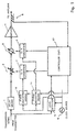
- Fig. 1 shows an example of circuitry of the amplifying device having the predistorter of the example (an amplifier with predistortion function).
- This amplifying device is provided in the transmission section of a base station or repeater station, for example, in a mobile wireless communication system, and the signal to be transmitted (transmission signal) is entered from a transmitter, and this signal is amplified in the amplifier, and sent out to an antenna.
- the amplifying device of the example comprises delay means 1 for delaying the transmission signal until the predistortion described below is ready, a variable attenuator 2 for providing the transmission signal with correction AM-AM characteristic for predistortion, a variable phase shifter 3 for providing the transmission signal with correction AM-PM characteristic for predistortion, an amplifier 4 for amplifying the transmission signal to a predetermined transmission level, a level detector 5 for detecting the (envelope) level of the transmission signal, distortion extracting means 6 for extracting a distortion component signal from the output signal of the amplifier 4, two D/A converters 7, 8 for converting the digital output signal from a controller 12 into an analog signal, a clock source 9 for providing each digital device with a clock, two phase adjusting means 10, 11 for generating clocks of different phase from the clock generated by the clock source 9, and a controller 12 for adaptively controlling the predistortion and controlling the phase adjusting means 10, 11.
- the signal to be transmitted issued from the transmitter is entered (in the amplifying device of this embodiment), and this signal is distributed into two, and one distribution signal is entered in the delay means 1 and the other distribution signal is fed into the level detector 5.
- the delay means 1 delays the input signal (one distribution signal) , and sends to the variable attenuator 2.
- the delay means 1 may be composed, for example, by using a delay wire for delaying a signal, or a band pass filter (BPF).
- variable attenuator 2 changes (attenuates) the amplitude of the signal entered from the delay means 1, depending on the (analog voltage) control signal entered from the D/A converter 7 described below to generate an amplitude distortion in an amount corresponding to the control signal to the input signal, and sends this signal (including amplitude distortion) to the variable phase shifter 3.
- variable phase shifter 3 changes the phase of the signal entered from the variable attenuator 2 depending on the (analog voltage) control signal entered from the D/A converter 8 described below to generate a phase distortion in an amount corresponding to the control signal to the input signal, and sends this signal (including phase distortion) to the amplifier 4.
- the predistorter is composed of the variable attenuator 2 and variable phase shifter 3 connected in series and control systems 1, 5 to 12 for controlling them.
- the amplifier 4 is composed of, for example, a (large) power amplifier, and amplifies the input signal from the variable phase shifter 3 to a desired (power) level, and sends out the amplified signal (from the amplifying device of the embodiment) to the antenna.
- the distortion component is compensated by generating a distortion of reverse characteristic (amplitude distortion or phase distortion) to the distortion occurring in the amplifier 4 by the predistorter (variable attenuator 2 and variable phase shifter 3).
- the level detector 5 is composed of, for example, an envelope detector for detecting the envelope of a signal by using a diode, a low pass filter (LPF) for extracting a specific frequency component only about the detected envelope, and an A/D converter for converting the detected envelope component from analog to digital signal.
- the reason of detecting the level of the input signal by the level detector 5 is, in the predistortion of the present embodiment, to correct the output level fluctuation or output phase fluctuation occurring in the amplifier 4 varying depending on the level of the input signal (in the amplifier 4), that is, it is necessary to detect the level of the transmission signal entered in the amplifier 4 (detected indirectly in this embodiment).
- the distortion extracting means 6 is composed of, for example, a directional coupler, and extracts distortion (for example, part of the amplified signal) included in the amplified signal issued from the amplifier 4, and sends out to the controller 12.
- the D/A converter 7 converts the digital control signal entered from the controller 12 described below into an analog control signal, according to the timing corresponding to the clock signal (timing signal) entered from the phase adjusting means 10 described below, and issues to the variable attenuator 2.
- This control signal is for controlling the amplitude change amount (that is, the amount of amplitude distortion to be generated) in the variable attenuator 2.
- the D/A converter 8 converts the digital control signal entered from the controller 12 described below into an analog control signal, according to the timing corresponding to the clock signal (timing signal) entered from the phase adjusting means 11 described below, and issues to the variable phase shifter 3.
- This control signal is for controlling the phase change amount (that is, the amount of phase distortion to be generated) in the variable phase shifter 3.
- the clock source 9 generates a clock signal of a predetermined period, and issues and supplies the clock signal into digital processing parts (excluding two D/A converters 7, 8 in this embodiment) such as the level detector 5 and two phase adjusting means 10, 11 described below.
- the phase adjusting means 10 generates a clock signal (timing shifted clock) shifted in phase from the clock signal entered from the clock source 9, according to the control from the controller 12, and sends this clock signal (timing signal) to the D/A converter 7.
- the phase adjusting means 11 generates a clock signal (timing shifted clock) shifted in phase from the clock signal entered from the clock source 9, according to the control from the controller 12, and sends this clock signal (timing signal) to the D/A converter 8.
- the controller 12 is composed of, for example, a digital signal processor (DSP). On the basis of the detection result (detected level) entered from the level detector 5, the controller 12 sends a digital control signal for realizing the amplitude change amount corresponding to the detection result to the D/A converter 7 from the variable attenuator 2, and sends the digital control signal for realizing the phase change amount corresponding to the detection result to the D/A converter 8 from the variable phase shifter 3.
- DSP digital signal processor
- the controller 12 since the level of the output signal is not linear to the level of the input signal (AM-AM conversion), amplitude distortion occurs, and since the phase of the output signal is not linear to the level of the input signal (AM-PM conversion), phase distortion occurs, and the amount of the generated amplitude distortion or phase distortion varies depending on the level of the signal provided for the amplifier 4. Accordingly, the controller 12 generates an amplitude distortion of the amount for canceling the amplitude distortion generated in the amplifier 4 by the variable attenuator 2, on the basis of the result of detection by the level detector 5 which is the level reflecting the level of the signal provided for the amplifier 4, and generates the phase distortion of the amount for canceling the phase distortion occurring in the amplifier 4 by the variable phase shifter 3.
- the correction amplitude distortion characteristic (the characteristic reverse to the amplitude distortion) for compensating the amplitude distortion occurring in the amplifier 4 and the correction phase distortion characteristic (the characteristic reverse to the phase distortion) for compensating the phase distortion occurring in the amplifier 4 are preliminarily calculated (or measured), and a correction table storing the control value relating to the amplitude distortion and the control value relating to the phase distortion corresponding to each other, for example, with respect to the value of detection result by the level detector 5 is saved in the memory of the controller 12.
- the controller 12 reads out the control value relating to the amplitude distortion and the control value relating to the phase distortion corresponding to the value (digitized level information) of the detection result entered from the level detector 5 from the correction table, and issues these two control values to the respective D/A converters 7, 8 as a digital control signal for controlling the variable attenuator 2 and a digital control signal for controlling the variable phase shifter 3.
- the controller 12 detects the level (for example, power level) of the distortion component (signal component out of band of use) from the signal entered, for example, from the distortion extracting means 6, and can update the content of the correction table so that the level to be detected may be smaller (preferably minimum), that is, the distortion compensation amount may be larger, thereby enhancing the precision of distortion compensation. Moreover, since the value to be corrected (the content in the correction table) can be updated adaptively, it is possible to provide predistortion capable of coping with a very small error of delay time caused by, for example, temperature characteristic change or aging effect.
- the controller 12 controls the phase adjustment (of a clock signal) performed by the phase adjusting means 10, 11, by issuing control signals to the phase adjusting means 10, 11.
- the controller 12 of the present embodiment controls the phase adjustment so that the level of the distortion component detected from the signal entered from the distortion extracting means 6 may be smaller (preferably minimum).
- phase adjusting means 10, 11 which are characteristic components of the invention are described in further detail.
- the transmission signal is delayed by the delay means 1 for the preparation time of predistortion in the digital region.
- the timing of the signal portion to be entered in the variable attenuator 2 or variable phase shifter 3 through the delay means 1, and the timing of the variable attenuator 2 or variable phase shifter 3 controlled by the controller 12 according to the level of the signal portion should be the same time.
- the error of delay time by the delay means 1 is relatively large, such a (small) timing is adjusted by the two phase adjusting means 10, 11.
- a clock is supplied in the digital circuit, or analog interface such as an A/D converter or a D/A converter.
- the (relative) delay time can be adjusted only in the unit of 12.5 nsec.
- the amplifying device of the embodiment includes two phase adjustingmeans 10, 11, and the phase adjusting means 10 generates a clock signal of an independent phase of the clock signal from the clock source 9. That is, in this embodiment, the clock signal issued from the clock source 9 is fed into the phase adjusting means 10, 11, and the phase of the clock signal is finely (precisely) adjusted in the phase adjusting means 10, 11, and supplied into each of the D/A converters 7, 8.
- the delay time by the delay means 1 is too short or too long, for example, by controlling the phase adjusting means 10, 11 by the control signal from the controller 12, the delay time (control timing of variable attenuator 2 or variable phase shifter 3) can be corrected finely (precisely) relatively easily.
- predistortion process can be executed correctly at the timing for processing predistortion on each signal portion composing the transmission signal, and hence the leak power out of the band left over and contained in the output signal of the amplifier 4 can be sufficiently decreased.
- a skilled engineer used to adjust the above-described delay time finely (precisely) in about half day, but in the amplifying device of the embodiment, such fine adjustment is easily realized (for example, automatically by the controller 12).
- processing timing is adjusted independently on each one of the two D/A converters 7, 8.
- timing adjustment at the time of A/D conversion for example, at the time of output of detection result from the level detector 5
- the delay time is adjusted (simultaneously) on the two D/A converters 7, 8 provided immediately before the variable attenuator 2 and variable phase shifter 3, it is possible to adjust the delay time due to line difference, for example, in the digital circuit, and it is hence possible to absorb and eliminate the small (slight) time difference in the line up to the D/A converters 7, 8.
- the phase of the clock signal (timing signal) given to the D/A converters 7, 8 may be deviated by the portion corresponding to this deviation.
- phase adjusting means 10, 11 A specific example of circuitry and an example of operation of the phase adjusting means 10, 11 are shown below.
- the circuitry of the phase adjusting means 10, 11 is identical, and the phase adjusting means 10 is representatively explained below in the following circuitry example.
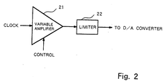
- Fig. 2 shows an example of circuitry of phase adjusting means 10, and this phase adjusting means 10 is composed of a series connection of a variable (gain) amplifier 21 and a limiter 22.
- the variable amplifier 21 has a characteristic of varying the gain depending on the control signal (for example, control voltage) entered from the controller 12, and amplifies the clock signal entered from the clock source 9 by the gain controlled by the controller 12, and sends the amplified signal to the limiter 22.
- control signal for example, control voltage
- the limiter 22 has a characteristic of issuing the levels of the signals, for example, when signals having levels over a (fixed) predetermined threshold are entered, all at the same level (for example, the level corresponding to the threshold), and limits the level of the amplified signal entered from the variable amplifier 21 by this characteristic, and sends the limited amplified signal to the D/A converter 7 (D/A converter 8 in the case of phase adjusting means 11).
- Fig. 3 (a) shows an example of waveform of a clock signal issued from the clock source 9.
- Fig. 3 (b) shows an example of waveform of a clock signal amplified by the variable amplifier 21.
- a solid line shows an example of waveform of a signal after the amplified clock signal is processed by the limiter 22, and for the convenience of explanation, further, an example of waveform of the amplified clock signal is indicated by a dotted line, together with an example of threshold set by the limiter 22.
- a dotted line shows an example of threshold set by the limiter 22.
- a solid line shows an example of waveform of a signal after processing of the amplified clock signal by the limiter 22, relating to the case of control of lower gain of the variable amplifier 21 as compared with the case of Fig. 3 (c), for the convenience of explanation and an example of waveform of the amplified clock signal is indicated by dotted line for reference, together with an example of threshold set in the limiter 22 (the same value as in (c)).
- a clock signal (timing signal) shifted in phase is generated and this signal is used as the input clock of the D/A converter 7, so that the operation timing of the D/A converter 7 can be (finely) adjusted. That is, since the D/A converter 7 operates at the timing of rise (or fall) of the clock signal being entered, and therefore it can be adjusted by slightly (precisely) changing the timing of output of the (analog) control signal from the D/A converter 7.
- phase adjusting means 10, 11 by controlling the gain of the variable amplifier 21 from the controller 12, clock signals (timing signals) having various phases can be generated, and hence the delay time can be adjusted finely (precisely).
- Fig. 4 shows other example of circuitry of the phase adjustingmeans 10, and this phase adjustingmeans 10 is composed by series connection of the amplifier 31 and comparator 32.
- the amplifier 31 has a characteristic of keeping constant, for example, the (voltage) level of the output signal (for example, the gain of amplification being constant), and it amplifies the clock signal entered from the clock source 9, and sends the amplified signal to the comparator 32.
- constant for example, the (voltage) level of the output signal (for example, the gain of amplification being constant)
- the amplifier 31 having such a characteristic is generally known as buffer, and such an amplifier 31 can be omitted from the circuitry as far as satisfying the condition that the phase adjustingmeans 10 is located physically close to the clock source 9, or the condition that the input signal into the phase adjusting means 10 (in this embodiment, the clock signal from the clock source 9) is not attenuated.
- the comparator 32 receives an amplified signal issued from the amplifier 31 and a control signal issued from the controller 12, and compares the level of these two signals, and produces the result of comparison as value 1 (for example, high level) or value 0 (for example, low level) to the D/A converter 7.
- the (voltage) level of the control signal entered from the controller 12 to the comparator 32 is used as the threshold in the comparator 32, and this comparator 32 produces an ON signal (signal of value 1 in this case) when the (voltage) level of the signal issued from the amplifier 31 is higher than the threshold, and an OFF signal (signal of value 0 in this case) when the level is less than the threshold.
- Fig. 5 shows another example of circuitry of the phase adjustingmeans 10, and this phase adjustingmeans 10 is composed of a series connection of an amplifier 41 and a limiter 42.
- the amplifier 41 has a characteristic of keeping constant, for example, the (voltage) level of the output signal (for example, the gain of amplification being constant), and it amplifies the clock signal entered from the clock source 9, and sends the amplified signal to the limiter 42.
- constant for example, the (voltage) level of the output signal (for example, the gain of amplification being constant)
- the limiter 42 has a characteristic of varying the threshold depending on the control signal entered from the controller 12, and when a signal having a level higher than the threshold is entered, it also has a characteristic of issuing the level of the signal all at the same level (for example, the level corresponding to the threshold), and the level of the amplified signal entered from the amplifier 41 is limited by this characteristic, and a controlled amplified signal is sent out to the D/A converter 7.
- the threshold of the limiter 42 is changed by the control (voltage) from the controller 12, and the limiter 42 limits the level when the (voltage) level of the signal entered from the amplifier 41 is over the threshold, and issues an ON signal (signal of value 1 in this case) at a specified (voltage) level.
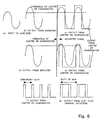
- FIG. 6 examples of operation of the circuit shown in Fig. 4 or Fig. 5 are presented.
- the circuit operation in Fig. 4 and the circuit operation in Fig. 5 have similar features, and operation examples of these two circuits are explained together.
- the lateral direction denotes the time and the vertical direction indicates the voltage level of a signal.
- Fig. 6 (f) and (g) are described in detail later.
- Fig. 6 (a) shows an example of waveform of a clock signal issued from the clock source 9 and entered in the amplifier (amplifier 31 or amplifier 41).
- Fig. 6 (b) and (d) show examples of waveform of a clock signal amplified (for example, provided with some fixed gain) by the amplifier (amplifier 31 or amplifier 41).
- Fig. 6 (c) and (e) show, by solid line, examples of waveform of signal issued from the phase adjusting means 10 (comparator 32 or limiter 42) to the D/A converter 7 when the threshold (of comparator 32 or limiter 42) is changed (in Fig. 6 (c) and (d)), and also show, by dotted line, examples of waveform of a clock signal provided for the amplifier (amplifier 31 or amplifier 41) for the convenience of explanation, and also examples of the threshold set (by the comparator 32 or limiter 42) are indicated by dotted line.
- phase adjusting means 10, 11, shown in Fig. 4 and Fig. 5 by controlling the threshold of the comparator 32 or threshold of the limiter 42 from the controller 12, clock signals (timing signals) having various phases can be generated, so that the delay time can be adjusted finely (precisely) . That is, in this embodiment, instead of varying the gain in the amplifier (amplifier 31 or amplifier 41), by varying the value (threshold) of the reference voltage to the comparator 32 in a later stage or the threshold of the limiter 42 in a later stage, the phase of the clock signal can be changed.
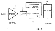
- Fig. 7 shows a different example of circuitry of the phase adjusting means 10, and this phase adjusting means 10 is composed of a series connection of a variable (gain) amplifier 51, alimiter 52, a flip-flop (D-FF) 53, and a selector 54.
- a variable (gain) amplifier 51 a variable (gain) amplifier 51
- alimiter 52 a flip-flop 53
- D-FF flip-flop
- the duty of the clock signal can be controlled by the flip-flop 53.
- the D/A converters 7, 8 operate on the rise or fall of the entered clock signal (timing signal), but in the actual D/A converter, the minimum required time (duty) is often specified, for example, in the high level region or low level region of the input clock.
- the phase variably shifted by the phase adjusting means 10 may be limited. In this structure, accordingly, the duty is shaped by the flip-flop 53.
- variable amplifier 51 The function and operation of the variable amplifier 51 are, for example, same as the function and operation of the variable amplifier 21 shown in Fig. 2, and the variable amplifier 51 amplifies the clock signal entered from the clock source 9 by the gain controlled by the controller 12, and sends the amplified signal to the limiter 52.
- the function and operation of the limiter 52 are same as the function and operation of the limiter 22 shown in Fig. 2, and the limiter 52 limits the level of the amplified signal entered from the variable amplifier 51 by a specified threshold, and sends the limited amplified signal to the flip-flop 53.
- the flip-flop 53 has two input ends and two output ends, and receives the signal issued from the limiter 52 at one input end, and receives an inverted signal issued from one output end (output end of inverted signal) at other input end, and sends out the inverted signal from one output end to the other input end and to the selector 54, and also sends a normal rotation signal out from the other output end to the selector 54.
- the normal rotation signal is, for example, a signal entered from the limiter 52 to the flip-flop 53 of which duty is changed by the flip-flop 53, and the inverted signal is the signal of which on/off state is inverted.
- the flip-flop 53 is generally used for setting the duty at 50%, and in the construction of this embodiment, the duty of the clock signal (timing signal) can be set to 50% as shown later in Fig. 8.
- the selector 54 has two input ends and one output end, and also has a function of changing over the output signal so that (only) the signal entered from either input end depending on the control signal from the controller 12 may be selectively issued from the output end.
- the selector 54 receives the inverted signal issued from one output end of the flip-flop 53 at one input end, and receives the normal rotation signal issued from the other output end of the flip-flop 53 at the other input end, and sends out either the inverted signal or normal rotation signal to the D/A converter 7 according to the control from the controller 12.
- Fig. 8 an operation example of the circuit shown in Fig. 7 is shown.
- the lateral direction indicates the time
- the vertical direction represents the voltage level of a signal.
- Fig. 8 (a) shows an example of waveform of a clock signal issued from the clock source 9 and entered in the variable amplifier 51.
- Fig. 8 (b) and (d) show examples of waveform of a clock signal provided for the variable amplifier 51 by using different gains (in Fig. 8 (b) and (d)).
- Fig. 8 (c) and (e), corresponding to Fig. 8 (b) and (d), show examples, indicated by solid line, of waveform of a signal after processing of the amplified clock signal by the limiter 52, and an example, indicated by dotted line, of waveform of the amplified clock signal and an example, indicted by dotted line, of threshold set in the limiter 52, by way of reference.
- the duty of the clock signal (timing signal) is set to 50% by the flip-flop 53.
- Fig. 8 (f) shows an example of waveform of the signal issued from the limiter 52, and at this stage, the duty of the signal varies depending on the (voltage) level of the signal issued from the variable amplifier 51.
- Fig. 8 (g) an example of waveform of a signal issued from the flip-flop 53 as, for example, normal rotation signal is indicated by solid line, and an example of waveform of a signal entered at one input end of the flip-flop 53 (as shown in Fig. 8 (f)) is indicated by dotted line for reference.
- the duty of the signal is 50 %.
- signals repeating on/off state at each rise point of the signal entered from the limiter 52 are issued, and the duty of such signals is 50%.
- the phase of the signal is shifted, but in the circuit structure of up to the flip-flop 53 mentioned above, it is hard to shift the phase by more than 180 degrees.
- the phase of the clock signal (timing signal) can be controlled by the selector 54 in a range of, for example, 360 degrees.
- the flip-flop 53 which generally produces a normal rotation signal and an inverted signal inverted in the rise time and fall time mutually, specifically, by controlling the selector 54 by the controller 12 so that either one of the normal rotation signal and inverted signal may be issued from the selector 54, the phase adjustment in a wide range can be realized.
- the clock source 9 is designed to produce a clock signal having a double speed (that is, half period) of the specified rate required in the input clock of, for example, the D/A converters 7, 8.
- the D/A conversion rate by the D/A converters 7, 8 is 80 MHz
- the clock source 9 for producing a clock signal of 160 MHz is used.
- the flip-flop 53 and selector 54 are added to the circuitry same as shown in Fig. 2, and similarly, it is possible to adjust the duty of the clock signal (timing signal) by installing a flip-flop in a later stage of the comparator 32 shown in Fig. 4 of in a later stage of the limiter 42 shown in Fig. 5, and further by installing a selector in a later stage of the flip-flop, it is also possible to expand the adjustable phase range in relation to the clock signal.
- Fig. 6 (f) shows an example of waveform of a signal issued from the comparator 32 or limiter 42, same as shown, for example, in Fig. 8 (f), and Fig. 6 (g) also shows, same as shown, for example, in Fig. 8 (g), an example of waveform of a signal converted by 50% in the duty of the signal by the flip-flop as indicated by solid line, and an example of waveform (in Fig. 6 (f)) of the signal before conversion as indicated by dotted line.
- the perturbation method is shown as an example of manner of adjusting the (relative) delay time by controlling the phase adjusting means 10, 11 by the controller 12.
- the distortion compensation by predistortion of the embodiment is conducted in conformity with the envelope of the signal to be amplified (by the amplifier 4).
- the control system of distortion compensation the system of the controller 12 or D/A converters 7, 8 side
- the main signal system in which the signal to be amplified flows the system of the variable attenuator 2 or variable phase shifter 3 side.
- a distortion component may be left over due to its effect in the signal issued from the amplifier 4 provided in a final stage. Presence or absence of such a distortion component can be easily judged by using a spectrum analyzer or the like, and the controller 12 in the embodiment detects the residual amount of distortion due to presence of delay time by monitoring the amount of distortion component by using the distortion extracting means 6.
- the delay time is adjusted by repeating the following process in (1) to (4).
- the updated delay time T is getting closer to the optimum state, and the difference between the distortion amount P0 and the distortion amount P+ or P- becomes smaller.
- the adjusting time used at step (2) or step (3) may be changed from ( ⁇ t) to ( ⁇ t/2) to reduce the adjusting time to half, so that the delay time can be adjusted adaptively.
- Fig. 9 shows an example of image of adjusting the delay time by perturbation method, in which the axis of abscissas denotes the (relative) delay time, the axis of ordinates in the upper direction represents the amount of distortion component, and the axis of ordinates in the lower direction shows the lapse of time.
- the diagram also includes a curve P showing the amount of distortion component (the distortion component extracted by the distortion extracting means 6) caused by the residual delay time, and the delay time becomes zero at a position of minimum distortion component amount.
- the position of the delay time T at the present moment is set as start point (point 1 in the diagram).
- the distortion amount at position of delay time (T+ ⁇ ) and the distortion amount at position of delay time (T- ⁇ ) are compared, and the delay time corresponding to the smaller distortion amount, for example, (T+ ⁇ ) is selected as an updated delay time T' (point 2).
- the distortion amount at position of delay time (T+ ⁇ + ⁇ ) and the distortion amount at position of delay time (T+ ⁇ - ⁇ ) are compared, and the delay time corresponding to the smaller distortion amount, for example, (T+ ⁇ + ⁇ ) is selected as an updated delay time T' (point 3).
- the distortion amount at position of delay time (T+ ⁇ + ⁇ + ⁇ /2) and the distortion amount at position of delay time (T+ ⁇ + ⁇ - ⁇ /2) are compared, and the delay time corresponding to the smaller distortion amount, for example, (T+ ⁇ + ⁇ - ⁇ /2) is selected as an updated delay time T' (point 4).
- the updated delay time is gradually set closer to the optimum delay time (zero).
- the delay time should be adjusted by a time error within, for example, [1/ ⁇ carrier frequency interval x number of carriers x n ⁇ ] (that is, in this embodiment, the difference from the optimum delay time of zero) .
- the carrier frequency interval and the number of carriers the values relating to the transmission signal to be processed by the amplifying device of the embodiment are used, and the value of n is a positive number of 8 or more.
- the product of (carrier frequency interval x number of carriers) corresponds to the band of the transmission signal.
- the timing can be adjusted finely (precisely), so that distortion compensation of high precision can be realized.
- the amplifier 4 corresponds to the amplifier (as the object of distortion compensation) of the invention.
- the distortion generating means of the invention is composed by the function of the variable attenuator 2 and variable phase shifter 3.
- the variable attenuator 2 and variable phase shifter 3 compose a circuit capable of changing the amount of distortion to be generated depending on the analog control signal entered from outside.
- the signal level detecting means of the invention is realized by the function of the level detector 5.
- the distortion amount control means of the invention is realized by the function of the controller 12 and two D/A converters 7, 8.
- control timing adjusting means of the invention is realized by the function of the clock source 9 and two phase adjusting means 10, 11.
- the D/A converting means of the invention is realized by the function of the two D/A converters 7, 8.
- the clock signal generating means of the invention is realized by the function of the clock source 9.
- the timing signal generating means of the invention is realized by the function of the two phase adjusting means 10, 11 for generating a clock signal (timing signal) adjusted in the timing.
- a (distortion compensation) amplifying device according to a second embodiment of the invention is explained below by referring to Fig. 10.
- the amplifying device of the embodiment has a predistorter which is an example of the distortion compensation apparatus of the invention, and the distortion occurring in the amplifier is compensated by the predistorter type distortion compensation system by using this predistorter.
- Fig. 10 shows an example of circuitry of an amplifying device having the predistorter of the embodiment (an amplifier with predistortion function).
- This amplifying device is provided in the transmission section of a base station or repeater station, for example, in a mobile wireless communication system, and the signal to be transmitted (transmission signal) is entered froma transmitter, and this signal is amplified in the amplifier, and sent out to an antenna.
- the amplifying device of the embodiment comprises delay means 61, variable attenuator 62, variable phase shifter 63, amplifier 64, level detector 65, distortion extracting means 66, two memories 67, 68, two D/A converters 69, 70, clock source 71, two phase adjusting means 72, 73, and controller 74.
- the composition of the amplifying device of the embodiment is similar to the composition of the amplifying device of the first embodiment shown in Fig. 1, except that the memories 67, 68 for controlling the variable attenuator 62 and variable phase shifter 63 are provided outside of the controller 74.
- the memories 67, 68 for controlling the variable attenuator 62 and variable phase shifter 63 are provided outside of the controller 74.
- same parts as in the amplifying device of first embodiment shown in Fig. 1 are not specifically described, and different parts as in the amplifying device of the first embodiment are described in detail.
- the memory 67 is provided between the controller 74 and the D/A converter 69
- the memory 68 is provided between the controller 74 and the D/A converter 70.
- the result of detecting the signal level by the level detector 65 is issued to the two memories 67, 68 as a digital value.
- One memory 67 has a look-up table (LUT) for controlling the variable attenuator 62, and this look-up table stores the (digital) control value for controlling the amplitude distortion to be generated in the variable attenuator 62, in correspondence to the digital value (of detection result) issued from the level detector 65.
- the control value the value for realizing the amplitude distortion (the amplitude distortion of reverse characteristic of the occurring amplitude distortion) capable of compensating the amplitude distortion occurring in the amplifier 64 by predistortion when the digital value (detection result) corresponding to the control value is obtained is, for example, preliminarily calculated (or measured) and stored.
- the other memory 68 has a look-up table (LUT) for controlling the variable phase shifter 63, and this look-up table stores the (digital) control value for controlling the phase distortion to be generated in the variable phase shifter 63, in correspondence to the digital value (of detection result) issued from the level detector 65.
- the control value the value for realizing the phase distortion (the phase distortion of reverse characteristic of the occurring phase distortion) capable of compensating the phase distortion occurring in the amplifier 64 by predistortion when the digital value (detection result) corresponding to the control value is obtained is, for example, preliminarily calculated (or measured) and stored.
- the memory 67 has a look-up table for storing the corrected AM-AM characteristic
- the other memory 68 has a look-up table for storing the corrected AM-PM characteristic.
- These look-up tables execute the process of issuing the stored value (control value) corresponding to the input address to the D/A converters 69, 70 respectively, using the digital value (control value) entered from the level detector 65a as the address, and in this embodiment, by such processing, the amount of distortion generated by the variable attenuator 62 and variable phase shifter 63 can be controlled.
- the D/A converters 69, 70 of the embodiment convert the digital control signals entered from the memories 67, 68 into analog control signals, and send the analog control signals to the variable attenuator 62 and variable phase shifter 63.
- the stored contents in the memories 67, 68 are adaptively rewritten by the controller 74, and such a constitution can realize predistortion capable of processing an error of a small delay time occurring due to, for example, temperature characteristic changes and aging effects.
- the memories 67, 68 for controlling the variable attenuator 62 and variable phase shifter 63 are composed separately from the controller 74 and disposed outside of the controller 74, fast access to the memories 67, 68 is possible, so that the efficiency of processing can be enhanced.
- the memory means of the invention is realized by the function of the two memories 67,68.
- the digital section operating at 80 MHz is assumed, but generally if D/Aconversionprocess at about 80MHz (12.5 nsec) is necessary, it is often difficult to access directly from the controller 74.
- the controller 74 is often composed of digital signal processor (DSP), and in the digital signal processor, the limit is about 30 MHz as the input and output rate (access speed of external hardware).
- DSP digital signal processor
- the amplifying device of the embodiment As mentioned above, fast access is possible by disposing the memories 67,68 outside of the controller 74, and in the case of processing a transmission signal of wide band, for example, fine (precise) phase adjustment (timing adjustment of D/A conversion) can be realized easily.
- the constitution of the distortion compensation apparatus according to the invention is not limited to the illustrated examples alone, but may be changed and modified in various forms.
- the sequence of disposition of the variable attenuator and variable phase shifter for predistortion is arbitrary.
- the structure for acquiring the signal (error signal) of distortion component from the output signal of the amplifier (as the object of distortion compensation), and the structure of level detector may be realized in various modes.
- a low pass filter may be provided between the D/A converter and variable attenuator, or between the D/A converter and variable phase shifter, and the output signals from these D/A converters may be smoothed by the low pass filter, and presence or absence of such low pass filter may be arbitrarily set depending on the situation of use of the device or the like.
- the application field of the distortion compensation apparatus of the invention is not limited to the shown fields alone, but the invention includes various other fields.
- the distortion compensation apparatus of the invention may be applied in the apparatus employing the predistortion type distortion compensation system using digital processing, and it is also possible to apply in the apparatus employing the predistortion type distortion compensation system using analog processing.
- the distortion compensation apparatus of the invention for example, in the hardware resource having a processor and memories, it may be designed to control by the processor which executes the control program stored in the ROM, or various function means for executing the processes may be composed as independent hardware circuits .
- the invention also relates to the computer-readable recording media, such as floppy disk and CD-ROM storing these control programs, and by feeding the control programs into the computer from the recording media, and executing by the processor, the process of the invention can be executed.
- the computer-readable recording media such as floppy disk and CD-ROM storing these control programs
- the compensation distortion apparatus of the invention for example, when controlling the amount of amplitude distortion or phase distortion generated by the variable attenuator or variable phase shifter on the signal to be provided for the amplifier, on the basis of the detection result of the level of the signal provided for the amplifier, the control timing is adjusted so that the distortion occurring in the amplitude may be compensated sufficiently, and it is possible to adjust the timing finely (precisely), so that distortion compensation of high precision is realized.
Landscapes
- Physics & Mathematics (AREA)
- Nonlinear Science (AREA)
- Engineering & Computer Science (AREA)
- Power Engineering (AREA)
- Amplifiers (AREA)
- Transmitters (AREA)
Applications Claiming Priority (2)
| Application Number | Priority Date | Filing Date | Title |
|---|---|---|---|
| JP2000260214 | 2000-08-30 | ||
| JP2000260214A JP3590571B2 (ja) | 2000-08-30 | 2000-08-30 | 歪補償装置 |
Publications (2)
| Publication Number | Publication Date |
|---|---|
| EP1191685A2 true EP1191685A2 (fr) | 2002-03-27 |
| EP1191685A3 EP1191685A3 (fr) | 2004-02-04 |
Family
ID=18748257
Family Applications (1)
| Application Number | Title | Priority Date | Filing Date |
|---|---|---|---|
| EP01302986A Withdrawn EP1191685A3 (fr) | 2000-08-30 | 2001-03-29 | Appareil de compensation de distorsion |
Country Status (3)
| Country | Link |
|---|---|
| US (2) | US6388518B1 (fr) |
| EP (1) | EP1191685A3 (fr) |
| JP (1) | JP3590571B2 (fr) |
Cited By (5)
| Publication number | Priority date | Publication date | Assignee | Title |
|---|---|---|---|---|
| EP1353439A2 (fr) * | 2002-04-10 | 2003-10-15 | Matsushita Electric Industrial Co., Ltd. | Dispositif pour la compensation des distorsions non-linéaires |
| EP1511180A1 (fr) * | 2002-05-31 | 2005-03-02 | Fujitsu Limited | Compensateur de distorsion |
| WO2005074123A1 (fr) * | 2004-01-30 | 2005-08-11 | Nokia Corporation | Circuit electronique |
| US7248112B2 (en) | 2002-05-14 | 2007-07-24 | Matsushita Electric Industrial Co., Ltd. | Hybrid distortion compensation method and hybrid distortion compensation device |
| US7551905B2 (en) | 2002-05-31 | 2009-06-23 | Fujitsu Limited | Distortion compensation apparatus |
Families Citing this family (73)
| Publication number | Priority date | Publication date | Assignee | Title |
|---|---|---|---|---|
| GB2358974B (en) * | 2000-02-01 | 2002-07-17 | Wireless Systems Int Ltd | Distortion reduction |
| JP2002223129A (ja) * | 2001-01-25 | 2002-08-09 | Hitachi Kokusai Electric Inc | プリディストーション方式増幅器及び包絡線検出装置 |
| US6731694B2 (en) * | 2001-08-07 | 2004-05-04 | Motorola, Inc. | Isolator eliminator for a linear transmitter |
| US6445249B1 (en) * | 2001-08-08 | 2002-09-03 | Motorola, Inc. | Modification of phase component of error signal to reduce variation of phase component of output signal of power amplifier |
| JP3643803B2 (ja) * | 2001-08-30 | 2005-04-27 | 株式会社日立国際電気 | 増幅装置 |
| JP2003078359A (ja) * | 2001-08-31 | 2003-03-14 | Hitachi Kokusai Electric Inc | 増幅装置 |
| US7218904B2 (en) * | 2001-10-26 | 2007-05-15 | Texas Instruments Incorporated | Removing close-in interferers through a feedback loop |
| JP2003168931A (ja) * | 2001-12-04 | 2003-06-13 | Nec Corp | 歪補償回路 |
| US7248642B1 (en) | 2002-02-05 | 2007-07-24 | Andrew Corporation | Frequency-dependent phase pre-distortion for reducing spurious emissions in communication networks |
| US7266159B2 (en) * | 2002-03-08 | 2007-09-04 | Andrew Corporation | Frequency-dependent magnitude pre-distortion on non-baseband input signals for reducing spurious emissions in communication networks |
| US7197085B1 (en) | 2002-03-08 | 2007-03-27 | Andrew Corporation | Frequency-dependent magnitude pre-distortion for reducing spurious emissions in communication networks |
| JP2003273659A (ja) * | 2002-03-15 | 2003-09-26 | Hitachi Kokusai Electric Inc | 歪補償増幅装置 |
| US6657490B2 (en) * | 2002-03-28 | 2003-12-02 | Motorola, Inc. | Feedforward signal generation for combined amplifiers |
| US6990143B2 (en) * | 2002-04-25 | 2006-01-24 | Broadcom, Corp. | 50% duty-cycle clock generator |
| US8380143B2 (en) | 2002-05-01 | 2013-02-19 | Dali Systems Co. Ltd | Power amplifier time-delay invariant predistortion methods and apparatus |
| US8811917B2 (en) | 2002-05-01 | 2014-08-19 | Dali Systems Co. Ltd. | Digital hybrid mode power amplifier system |
| US6985704B2 (en) | 2002-05-01 | 2006-01-10 | Dali Yang | System and method for digital memorized predistortion for wireless communication |
| US8472897B1 (en) | 2006-12-22 | 2013-06-25 | Dali Systems Co. Ltd. | Power amplifier predistortion methods and apparatus |
| US7139327B2 (en) * | 2002-06-10 | 2006-11-21 | Andrew Corporation | Digital pre-distortion of input signals for reducing spurious emissions in communication networks |
| JP3872726B2 (ja) * | 2002-06-12 | 2007-01-24 | 富士通株式会社 | 送信増幅器 |
| JP4282955B2 (ja) * | 2002-07-02 | 2009-06-24 | 株式会社日立国際電気 | 歪み補償装置 |
| US7212584B2 (en) * | 2002-08-05 | 2007-05-01 | Hitachi Kokusai Electric Inc. | Distortion compensator |
| JP2004186020A (ja) * | 2002-12-04 | 2004-07-02 | Matsushita Electric Ind Co Ltd | 操作突起付可動接点体およびその操作突起の装着方法、ならびにこれを用いた操作パネル用スイッチ |
| US7231573B2 (en) * | 2002-12-20 | 2007-06-12 | Verigy Pte. Ltd. | Delay management system |
| US6812792B2 (en) * | 2003-01-02 | 2004-11-02 | Harris Corporation | Precorrection of a nonlinear amplifier |
| US7403573B2 (en) * | 2003-01-15 | 2008-07-22 | Andrew Corporation | Uncorrelated adaptive predistorter |
| JP2004312344A (ja) * | 2003-04-07 | 2004-11-04 | Hitachi Kokusai Electric Inc | 歪補償装置 |
| KR100553270B1 (ko) * | 2003-05-16 | 2006-02-20 | 주식회사 에이스테크놀로지 | 출력 레벨 자동 설정 중계기 및 출력 레벨 자동 설정 방법 |
| US7251293B2 (en) * | 2003-06-27 | 2007-07-31 | Andrew Corporation | Digital pre-distortion for the linearization of power amplifiers with asymmetrical characteristics |
| US7026871B2 (en) * | 2003-07-03 | 2006-04-11 | Icefyre Semiconductor, Inc. | Adaptive predistortion for a transmit system |
| US6975167B2 (en) * | 2003-07-03 | 2005-12-13 | Icefyre Semiconductor Corporation | Adaptive predistortion for a transmit system with gain, phase and delay adjustments |
| US7453952B2 (en) * | 2003-07-03 | 2008-11-18 | Saed Aryan | Predistortion circuit for a transmit system |
| US7409193B2 (en) * | 2003-07-03 | 2008-08-05 | Zarbana Digital Fund Llc | Predistortion circuit for a transmit system |
| US7259630B2 (en) * | 2003-07-23 | 2007-08-21 | Andrew Corporation | Elimination of peak clipping and improved efficiency for RF power amplifiers with a predistorter |
| US7280612B2 (en) * | 2003-07-25 | 2007-10-09 | Zarbana Digital Fund Llc | Digital branch calibrator for an RF transmitter |
| US6885322B2 (en) * | 2003-08-05 | 2005-04-26 | Motorola, Inc. | Apparatus and method for transmitter phase shift compensation |
| JP3844352B2 (ja) | 2003-08-07 | 2006-11-08 | 松下電器産業株式会社 | 送信装置 |
| US7372917B2 (en) * | 2004-08-25 | 2008-05-13 | Broadcom Corporation | Digital algorithm for on-line ACPR optimization in polar RF transmitters |
| US7023273B2 (en) * | 2003-10-06 | 2006-04-04 | Andrew Corporation | Architecture and implementation methods of digital predistortion circuitry |
| JP2007521700A (ja) * | 2003-10-20 | 2007-08-02 | トムソン ライセンシング | 無線送信機に使用するための前置補償器 |
| JP2005150932A (ja) * | 2003-11-12 | 2005-06-09 | Hitachi Kokusai Electric Inc | プリディスト−ション装置 |
| JP4467319B2 (ja) * | 2004-01-29 | 2010-05-26 | 株式会社日立国際電気 | プリディストータ |
| US7250815B2 (en) * | 2004-02-25 | 2007-07-31 | Intel Corporation | Amplifier distortion management apparatus, systems, and methods |
| KR20070058376A (ko) * | 2004-03-25 | 2007-06-08 | 옵티크론, 인코포레이티드. | 아날로그-디지털 변환기 선형화를 위해 복잡성을 감소시킨비선형 필터들 |
| WO2005094536A2 (fr) * | 2004-03-25 | 2005-10-13 | Optichron, Inc. | Systeme de linearisation numerique |
| GB2414352A (en) * | 2004-05-18 | 2005-11-23 | Roke Manor Research | An adaptively-corrected RF pulse amplifier for a beam-steered radar antenna array |
| US7239671B2 (en) * | 2004-07-09 | 2007-07-03 | Powerwave Technologies, Inc. | System and method for digital timing error correction in a communications system utilizing adaptive predistortion |
| US7352226B2 (en) * | 2004-08-02 | 2008-04-01 | Raytheon Company | Versatile attenuator |
| US7486939B2 (en) * | 2005-06-21 | 2009-02-03 | Motorola, Inc. | Apparatus for removing distortions created by an amplifier |
| US7782978B2 (en) * | 2006-04-13 | 2010-08-24 | Harris Corporation | Phase correction of a constant envelope signal without introducing amplitude modulation |
| CN101479956B (zh) | 2006-04-28 | 2013-07-31 | 大力系统有限公司 | 用于无线通信的高效率线性化功率放大器 |
| US7689179B2 (en) * | 2006-07-03 | 2010-03-30 | Panasonic Corporation | Multistage amplifier apparatus with distortion compensation function |
| US7729670B2 (en) * | 2006-09-29 | 2010-06-01 | Broadcom Corporation | Method and system for minimizing power consumption in a communication system |
| EP3416340B1 (fr) * | 2006-12-26 | 2020-10-21 | Dali Systems Co., Ltd. | Procédé et système de linéarisation de prédistorsion de bande de base dans des systèmes de communication large bande multicanaux |
| US7925170B2 (en) * | 2007-08-07 | 2011-04-12 | Applied Optoelectronics, Inc. | Predistortion circuit including distortion generator diodes with adjustable diode bias |
| US8073340B2 (en) | 2008-02-05 | 2011-12-06 | Applied Optoelectronics, Inc. | Distortion compensation circuit including one or more phase invertible distortion paths |
| US8121493B2 (en) * | 2008-02-05 | 2012-02-21 | Applied Optoelectronics, Inc. | Distortion compensation circuit and method based on orders of time dependent series of distortion signal |
| JP5176692B2 (ja) * | 2008-05-28 | 2013-04-03 | 日本電気株式会社 | 歪補償回路及び歪補償方法 |
| JP2011082953A (ja) * | 2009-09-10 | 2011-04-21 | Sumitomo Electric Ind Ltd | 増幅装置、及びこれを用いた無線送信装置 |
| JP4792530B2 (ja) * | 2010-03-08 | 2011-10-12 | 株式会社アドバンテスト | レーザ光パルスの位相制御装置 |
| CN103597807B (zh) | 2010-09-14 | 2015-09-30 | 大理系统有限公司 | 远程可重新配置的分布式天线系统和方法 |
| US8606116B2 (en) | 2011-01-13 | 2013-12-10 | Applied Optoelectronics, Inc. | System and method for distortion compensation in response to frequency detection |
| EP2665803B1 (fr) | 2011-01-23 | 2020-03-25 | Pike Enterprises, LLC | Système de pyrolyse autonome pour génération d'énergie |
| US20120242405A1 (en) * | 2011-03-25 | 2012-09-27 | Younkyu Chung | Frequency-Desensitizer for Broadband Predistortion Linearizers |
| US8711976B2 (en) | 2011-05-12 | 2014-04-29 | Andrew Llc | Pre-distortion architecture for compensating non-linear effects |
| JP2013013026A (ja) * | 2011-06-30 | 2013-01-17 | Toshiba Corp | 送信装置とその歪み補償方法 |
| US8514007B1 (en) | 2012-01-27 | 2013-08-20 | Freescale Semiconductor, Inc. | Adjustable power splitter and corresponding methods and apparatus |
| US8891974B2 (en) | 2012-03-30 | 2014-11-18 | Applied Optoelectronics, Inc. | Distortion compensation circuit including tunable phase path |
| JP6281196B2 (ja) * | 2013-07-19 | 2018-02-21 | 富士通株式会社 | 位相補償回路、エンファシス信号生成回路および位相補償方法 |
| JP6252226B2 (ja) * | 2014-02-17 | 2017-12-27 | 富士通株式会社 | 歪補償装置、無線送信装置及び歪補償方法 |
| US9774299B2 (en) | 2014-09-29 | 2017-09-26 | Nxp Usa, Inc. | Modifiable signal adjustment devices for power amplifiers and corresponding methods and apparatus |
| US9998241B2 (en) * | 2015-02-19 | 2018-06-12 | Mediatek Inc. | Envelope tracking (ET) closed-loop on-the-fly calibration |
| US9647611B1 (en) | 2015-10-28 | 2017-05-09 | Nxp Usa, Inc. | Reconfigurable power splitters and amplifiers, and corresponding methods |
Citations (3)
| Publication number | Priority date | Publication date | Assignee | Title |
|---|---|---|---|---|
| US5489875A (en) * | 1994-09-21 | 1996-02-06 | Simon Fraser University | Adaptive feedforward linearizer for RF power amplifiers |
| WO2000031881A1 (fr) * | 1998-11-19 | 2000-06-02 | Cadence Design Systems Inc. | Amplificateur de puissance rf lineaire et emetteur |
| US6112062A (en) * | 1997-09-26 | 2000-08-29 | The Whitaker Corporation | Predistortion for high power amplifiers |
Family Cites Families (8)
| Publication number | Priority date | Publication date | Assignee | Title |
|---|---|---|---|---|
| US5101173A (en) * | 1990-11-28 | 1992-03-31 | The United States Of America As Represented By The Secretary Of The Air Force | Stored program controlled module amplifier bias and amplitude/phase compensation apparatus |
| FR2746564B1 (fr) * | 1996-03-22 | 1998-06-05 | Matra Communication | Procede pour corriger des non-linearites d'un amplificateur, et emetteur radio mettant en oeuvre un tel procede |
| AU3339397A (en) * | 1996-06-19 | 1998-01-07 | Fraunhofer-Gesellschaft Zur Forderung Der Angewandten Forschung E.V. | Pre-distortion for a non-linear transmission path in the high frequency range |
| US6075411A (en) * | 1997-12-22 | 2000-06-13 | Telefonaktiebolaget Lm Ericsson | Method and apparatus for wideband predistortion linearization |
| US5929704A (en) * | 1998-02-20 | 1999-07-27 | Spectrian | Control of RF error extraction using auto-calibrating RF correlator |
| US6188277B1 (en) * | 1998-08-19 | 2001-02-13 | Harris Corporation | Power amplifier having monitoring and circuit protection |
| JP3241012B2 (ja) * | 1998-11-26 | 2001-12-25 | 日本電気株式会社 | 送信時消費電力低減回路及びこれを用いた無線通信装置並びに線形動作制御方法 |
| US6275685B1 (en) * | 1998-12-10 | 2001-08-14 | Nortel Networks Limited | Linear amplifier arrangement |
-
2000
- 2000-08-30 JP JP2000260214A patent/JP3590571B2/ja not_active Expired - Fee Related
-
2001
- 2001-03-28 US US09/818,898 patent/US6388518B1/en not_active Expired - Lifetime
- 2001-03-29 EP EP01302986A patent/EP1191685A3/fr not_active Withdrawn
- 2001-12-31 US US10/029,918 patent/US6677820B2/en not_active Expired - Fee Related
Patent Citations (3)
| Publication number | Priority date | Publication date | Assignee | Title |
|---|---|---|---|---|
| US5489875A (en) * | 1994-09-21 | 1996-02-06 | Simon Fraser University | Adaptive feedforward linearizer for RF power amplifiers |
| US6112062A (en) * | 1997-09-26 | 2000-08-29 | The Whitaker Corporation | Predistortion for high power amplifiers |
| WO2000031881A1 (fr) * | 1998-11-19 | 2000-06-02 | Cadence Design Systems Inc. | Amplificateur de puissance rf lineaire et emetteur |
Non-Patent Citations (1)
| Title |
|---|
| YU D ET AL: "A digital phase and amplitude feedforward correction system" , PARTICLE ACCELERATOR CONFERENCE, 1993., PROCEEDINGS OF THE 1993 WASHINGTON, DC, USA 17-20 MAY 1993, NEW YORK, NY, USA,IEEE, PAGE(S) 2388-2390 XP010112068 ISBN: 0-7803-1203-1 * the whole document * * |
Cited By (8)
| Publication number | Priority date | Publication date | Assignee | Title |
|---|---|---|---|---|
| EP1353439A2 (fr) * | 2002-04-10 | 2003-10-15 | Matsushita Electric Industrial Co., Ltd. | Dispositif pour la compensation des distorsions non-linéaires |
| EP1353439A3 (fr) * | 2002-04-10 | 2007-11-28 | Matsushita Electric Industrial Co., Ltd. | Dispositif pour la compensation des distorsions non-linéaires |
| US7248112B2 (en) | 2002-05-14 | 2007-07-24 | Matsushita Electric Industrial Co., Ltd. | Hybrid distortion compensation method and hybrid distortion compensation device |
| EP1511180A1 (fr) * | 2002-05-31 | 2005-03-02 | Fujitsu Limited | Compensateur de distorsion |
| EP1511180A4 (fr) * | 2002-05-31 | 2006-02-15 | Fujitsu Ltd | Compensateur de distorsion |
| US7551905B2 (en) | 2002-05-31 | 2009-06-23 | Fujitsu Limited | Distortion compensation apparatus |
| WO2005074123A1 (fr) * | 2004-01-30 | 2005-08-11 | Nokia Corporation | Circuit electronique |
| US7113035B2 (en) | 2004-01-30 | 2006-09-26 | Nokia Corporation | Electronic circuit |
Also Published As
| Publication number | Publication date |
|---|---|
| JP2002076785A (ja) | 2002-03-15 |
| EP1191685A3 (fr) | 2004-02-04 |
| US20020041209A1 (en) | 2002-04-11 |
| US6677820B2 (en) | 2004-01-13 |
| US6388518B1 (en) | 2002-05-14 |
| JP3590571B2 (ja) | 2004-11-17 |
| US20020079964A1 (en) | 2002-06-27 |
Similar Documents
| Publication | Publication Date | Title |
|---|---|---|
| US6388518B1 (en) | Distortion compensation apparatus | |
| US7072420B2 (en) | Communications systems | |
| US7535310B2 (en) | Distortion compensation circuit | |
| EP2027649B1 (fr) | Système et procédé pour constituer un circuit émetteur pour une modulation polaire et une linéarisation d'amplificateur de puissance | |
| AU2007211189B2 (en) | Supply voltage control for a power amplifier | |
| GB2265269A (en) | Radio transmitter with linearization training sequence | |
| WO1997043824A1 (fr) | Amplificateur a pre/post-distorsion | |
| JPH08504074A (ja) | 通信装置内の制御ループの利得を安定させる方法および装置 | |
| TW423232B (en) | Method for adaptively controlling amplifier linearization devices | |
| US7289777B2 (en) | Power control for non-constant envelope modulation | |
| US6904268B2 (en) | Low noise linear transmitter using cartesian feedback | |
| EP1235344B1 (fr) | Procédé de réduction d'interférence dans un émetteur | |
| JP3606573B2 (ja) | 歪補償装置 | |
| EP1611675B1 (fr) | Amplificateur de puissance et emetteur radioelectrique et terminal presentant ledit amplificateur | |
| JP2004336428A (ja) | 歪補償回路 | |
| WO2008021705A2 (fr) | Transmetteur linéarisé et procédé de fonctionnement pour utilisation en communication sans fil | |
| JPH07123065A (ja) | 時分割多重アクセス無線装置 | |
| JP2004032584A (ja) | 歪補償回路 | |
| JP2004312527A (ja) | 高周波増幅装置 |
Legal Events
| Date | Code | Title | Description |
|---|---|---|---|
| PUAI | Public reference made under article 153(3) epc to a published international application that has entered the european phase |
Free format text: ORIGINAL CODE: 0009012 |
|
| AK | Designated contracting states |
Kind code of ref document: A2 Designated state(s): AT BE CH CY DE DK ES FI FR GB GR IE IT LI LU MC NL PT SE TR |
|
| AX | Request for extension of the european patent |
Free format text: AL;LT;LV;MK;RO;SI |
|
| PUAL | Search report despatched |
Free format text: ORIGINAL CODE: 0009013 |
|
| AK | Designated contracting states |
Kind code of ref document: A3 Designated state(s): AT BE CH CY DE DK ES FI FR GB GR IE IT LI LU MC NL PT SE TR |
|
| AX | Request for extension of the european patent |
Extension state: AL LT LV MK RO SI |
|
| AKX | Designation fees paid | ||
| REG | Reference to a national code |
Ref country code: DE Ref legal event code: 8566 |
|
| STAA | Information on the status of an ep patent application or granted ep patent |
Free format text: STATUS: THE APPLICATION IS DEEMED TO BE WITHDRAWN |
|
| 18D | Application deemed to be withdrawn |
Effective date: 20040805 |