EP1190436B1 - Plasma processor with coil responsive to variable amplitude rf envelope - Google Patents
Plasma processor with coil responsive to variable amplitude rf envelope Download PDFInfo
- Publication number
- EP1190436B1 EP1190436B1 EP00946836A EP00946836A EP1190436B1 EP 1190436 B1 EP1190436 B1 EP 1190436B1 EP 00946836 A EP00946836 A EP 00946836A EP 00946836 A EP00946836 A EP 00946836A EP 1190436 B1 EP1190436 B1 EP 1190436B1
- Authority
- EP
- European Patent Office
- Prior art keywords
- coil
- plasma
- amplitude
- workpiece
- envelope
- Prior art date
- Legal status (The legal status is an assumption and is not a legal conclusion. Google has not performed a legal analysis and makes no representation as to the accuracy of the status listed.)
- Expired - Lifetime
Links
- 230000004907 flux Effects 0.000 claims description 35
- 230000005284 excitation Effects 0.000 claims description 23
- 238000000034 method Methods 0.000 claims description 20
- 230000002093 peripheral effect Effects 0.000 claims description 17
- 239000002245 particle Substances 0.000 claims description 15
- 238000012545 processing Methods 0.000 claims description 15
- 239000002184 metal Substances 0.000 claims description 6
- 230000008859 change Effects 0.000 claims description 5
- 210000002381 plasma Anatomy 0.000 description 144
- 239000007789 gas Substances 0.000 description 19
- 238000005530 etching Methods 0.000 description 12
- 150000002500 ions Chemical class 0.000 description 8
- 239000003990 capacitor Substances 0.000 description 7
- 238000009792 diffusion process Methods 0.000 description 7
- 230000006870 function Effects 0.000 description 7
- 238000002474 experimental method Methods 0.000 description 6
- 239000000463 material Substances 0.000 description 6
- 230000008569 process Effects 0.000 description 5
- VYPSYNLAJGMNEJ-UHFFFAOYSA-N silicon dioxide Inorganic materials O=[Si]=O VYPSYNLAJGMNEJ-UHFFFAOYSA-N 0.000 description 5
- 239000000758 substrate Substances 0.000 description 4
- 230000005540 biological transmission Effects 0.000 description 3
- 230000007423 decrease Effects 0.000 description 3
- 230000005686 electrostatic field Effects 0.000 description 3
- 239000003574 free electron Substances 0.000 description 3
- 238000005259 measurement Methods 0.000 description 3
- 238000003672 processing method Methods 0.000 description 3
- 230000009467 reduction Effects 0.000 description 3
- 239000004065 semiconductor Substances 0.000 description 3
- 235000012239 silicon dioxide Nutrition 0.000 description 3
- XKRFYHLGVUSROY-UHFFFAOYSA-N Argon Chemical compound [Ar] XKRFYHLGVUSROY-UHFFFAOYSA-N 0.000 description 2
- XUIMIQQOPSSXEZ-UHFFFAOYSA-N Silicon Chemical compound [Si] XUIMIQQOPSSXEZ-UHFFFAOYSA-N 0.000 description 2
- 238000010521 absorption reaction Methods 0.000 description 2
- 230000008901 benefit Effects 0.000 description 2
- 230000008033 biological extinction Effects 0.000 description 2
- 229910052681 coesite Inorganic materials 0.000 description 2
- 230000008878 coupling Effects 0.000 description 2
- 238000010168 coupling process Methods 0.000 description 2
- 238000005859 coupling reaction Methods 0.000 description 2
- 229910052906 cristobalite Inorganic materials 0.000 description 2
- 238000001035 drying Methods 0.000 description 2
- 230000000694 effects Effects 0.000 description 2
- 230000005684 electric field Effects 0.000 description 2
- 238000009616 inductively coupled plasma Methods 0.000 description 2
- 230000007246 mechanism Effects 0.000 description 2
- 229910052710 silicon Inorganic materials 0.000 description 2
- 239000010703 silicon Substances 0.000 description 2
- 239000000377 silicon dioxide Substances 0.000 description 2
- 229910052682 stishovite Inorganic materials 0.000 description 2
- 229910052905 tridymite Inorganic materials 0.000 description 2
- 238000012935 Averaging Methods 0.000 description 1
- ZAMOUSCENKQFHK-UHFFFAOYSA-N Chlorine atom Chemical compound [Cl] ZAMOUSCENKQFHK-UHFFFAOYSA-N 0.000 description 1
- 230000009471 action Effects 0.000 description 1
- 229910052786 argon Inorganic materials 0.000 description 1
- 239000000460 chlorine Substances 0.000 description 1
- 229910052801 chlorine Inorganic materials 0.000 description 1
- 238000000151 deposition Methods 0.000 description 1
- 238000010586 diagram Methods 0.000 description 1
- 239000003989 dielectric material Substances 0.000 description 1
- 230000005672 electromagnetic field Effects 0.000 description 1
- 238000005516 engineering process Methods 0.000 description 1
- 239000011521 glass Substances 0.000 description 1
- 230000006872 improvement Effects 0.000 description 1
- 238000000059 patterning Methods 0.000 description 1
- 230000000737 periodic effect Effects 0.000 description 1
- 238000001020 plasma etching Methods 0.000 description 1
- 229910021420 polycrystalline silicon Inorganic materials 0.000 description 1
- 238000006116 polymerization reaction Methods 0.000 description 1
- 239000010453 quartz Substances 0.000 description 1
- 230000004044 response Effects 0.000 description 1
- 238000007789 sealing Methods 0.000 description 1
- 239000007787 solid Substances 0.000 description 1
- 230000001360 synchronised effect Effects 0.000 description 1
Images

Classifications
-
- H—ELECTRICITY
- H01—ELECTRIC ELEMENTS
- H01L—SEMICONDUCTOR DEVICES NOT COVERED BY CLASS H10
- H01L21/00—Processes or apparatus adapted for the manufacture or treatment of semiconductor or solid state devices or of parts thereof
-
- H—ELECTRICITY
- H01—ELECTRIC ELEMENTS
- H01J—ELECTRIC DISCHARGE TUBES OR DISCHARGE LAMPS
- H01J37/00—Discharge tubes with provision for introducing objects or material to be exposed to the discharge, e.g. for the purpose of examination or processing thereof
- H01J37/32—Gas-filled discharge tubes
- H01J37/32009—Arrangements for generation of plasma specially adapted for examination or treatment of objects, e.g. plasma sources
- H01J37/32082—Radio frequency generated discharge
- H01J37/32137—Radio frequency generated discharge controlling of the discharge by modulation of energy
- H01J37/32146—Amplitude modulation, includes pulsing
-
- H—ELECTRICITY
- H01—ELECTRIC ELEMENTS
- H01J—ELECTRIC DISCHARGE TUBES OR DISCHARGE LAMPS
- H01J37/00—Discharge tubes with provision for introducing objects or material to be exposed to the discharge, e.g. for the purpose of examination or processing thereof
- H01J37/32—Gas-filled discharge tubes
- H01J37/32009—Arrangements for generation of plasma specially adapted for examination or treatment of objects, e.g. plasma sources
- H01J37/32082—Radio frequency generated discharge
- H01J37/321—Radio frequency generated discharge the radio frequency energy being inductively coupled to the plasma
Definitions
- the present invention relates generally to plasma processors including radio frequency (r.f.) responsive coils for exciting gases in vacuum chambers to plasmas that process workpieces in the chamber and more particularly to such a processor and to a processing method wherein plasma density on the workpiece is controlled by varying the amplitude of the envelope of the r.f. applied to the coil.
- radio frequency r.f.
- One type of processor for treating workpieces with an r.f. plasma in a vacuum chamber includes a coil responsive to an r.f. source.
- the coil responds to the r.f. source to produce magnetic and electric fields that excite ionizable gas in the chamber to a plasma.
- the coil is on or adjacent to a dielectric window that extends in a direction generally parallel to a planar horizontally extending surface of the processed workpiece.
- the excited plasma interacts with the workpiece in the chamber to etch the workpiece or to deposit material on it.
- the workpiece is typically a semiconductor wafer having a planar circular surface or a solid dielectric plate, e.g., a rectangular glass substrate used in flat panel displays, or a metal plate.
- U.S. Patent 4,948,458 discloses a multi-turn spiral coil for achieving the above results.
- the spiral which is generally of the Archimedes type, extends radially and circumferentially between its interior and exterior terminals connected to the r.f. source via an impedance matching network.
- Coils of this general type produce oscillating r.f. fields having magnetic and capacitive field components that propagate through the dielectric window to heat electrons in the gas in a portion of the plasma in the chamber close to the window.
- the oscillating r.f. fields induce in the plasma currents that heat electrons in the plasma.
- the spatial distribution of the magnetic field in the plasma portion close to the window is a function of the sum of individual magnetic field components produced by each turn of the coil.
- the magnetic field component produced by each of the turns is a function of the magnitude of r.f. current in each turn which differs for different turns because of transmission line effects of the coil at the frequency of the r.f. source.
- the r.f. currents in the spiral coil are distributed to produce a torroidal shaped magnetic field region in the portion of the plasma close to the window, which is where power is absorbed by the gas to excite the gas to a plasma.
- diffusion of the plasma from the ring shaped region produces plasma density peaks just above the workpiece in central and peripheral portions of the chamber, so the peak densities of the ions and electrons which process the workpiece are in proximity to the workpiece center line and workpiece periphery.
- the coil of the '280 patent produces considerably smaller plasma flux variations across the workpiece than the coil of the '458 patent.
- the standard deviation of the plasma flux produced by the coil of the '280 patent on a 200 mm wafer in such a chamber operating at 0.7 Pa (5 milliTorr) is about 2.0, a considerable improvement over the standard deviation of approximately 3.0 for a coil of the '458 patent operating under the same conditions.
- the coil of the '280 patent causes the magnetic field to be such that the plasma density in the center of the workpiece is greater than in an intermediate part of the workpiece, which in turn exceeds the plasma density in the periphery of the workpiece.
- the plasma density variations in the different portions of the chamber for the coil of the '280 patent are much smaller than those of the coil of the '458 patent for the same operating conditions as produce the lower standard deviation.
- US 5,897,713 A discloses a planar coil that consists of five concentric arcuate elements. The coil is arranged on a dielectric plate that surrounds a part of the plasma process room and is connected to an RF power supply. US 5,897,713 A also discloses to improve the uniformity of the spatial distribution of a plasma by modulating the RF wave applied to such a coil.
- An additional object of the present invention to provide a new and improves vacuum plasma processor and method of operating same wherein the plasma density incident on the workpieces has relatively high uniformity.
- Another object of the invention is to provide a new and improved vacuum plasma processor having the same geometry as the prior art but which is operated to have controlled plasma density characteristics.
- An added object of the invention in to provide a new and improved vacuum plasma processor having the same geometry as the prior art but which is operated to have greater plasma density uniformity characteristics than the prior art.
- a further object of the invention is to provides a new and improved vacuum plasma processor including an r.f. excitation coil that is operated so the plasma density has a standard deviation across the workpiece less than 2.0.
- a vacuum plasma processor for processing workpieces comprising a vacuum chamber for processing the workpieces with a plasma, a holder in the chamber for the workpieces, a coil for exciting gas in the chamber into the plasma, an r. f. source for supplying to the coil an r. f. carrier having a variable amplitude envelope in the form of pulses; the coil including first and second interior arcuate segments and also exterior arcuate segments radially displaced from the interior arcuate segments and first and second excitation terminals at respective ends of the coil and adapted to be connected to the r.f.
- the first and second interior arcuate segments being connected to each other by way of the exterior arcuate segments, the first terminal being at one end of the coil and at one end of the first interior arcuate segment and the second terminal being at one end of the second interior arcuate segment, the variable amplitude, pressure within the chamber, and the arrangement of (a) the coil, (b) the chamber and (c) the holder being such that the plasma has a higher density on a portion of the workpiece aligned with a center portion of the coil than on a portion of the workpiece aligned with a portion of the coil removed from the center portion of the coil when a constant amplitude r.f. envelope is supplied to the coil, the r. f.
- variable amplitude envelope has low amplitude portions of sufficient duration and magnitude to enable charge particles in the plasma to diffuse in the chamber and thereby cause the plasma density in a portion of the workpiece removed from the portion of the workpiece aligned with the center portion of the coil to be at least equal to the plasma density in the portion of the workpiece aligned with the center portion of the coil.
- a method of plasma processing a workpiece on a holder in a vacuum plasma processor chamber comprising exciting gas in the chamber to a plasma by applying an r.f. carrier having envelope amplitude variations to a coil which responds to the r.f. carrier to couple magnetic and electric plasma excitation fields to the plasma, the coil including first and second interior arcuate segments and also exterior arcuate segments radially displaced from the interior arcuate segments, and first and second excitation terminals at respective ends of the coil and adapted to be connected to the r.f.
- the first and second interior arcuate segments being connected to each other by way of the exterior arcuate segments, the first excitation terminal being at one end of the first interior arcuate segment, and the second excitation terminal being at one end of the second interior segment, and the envelope variations having low amplitude portions of sufficient duration and magnitude to enable charge particles in the plasma to diffuse in the chamber so as to serve to maintain the density of the plasma across the workpiece substantially constant also by control of the coil, chamber, workpiece and holder parameters, such that the density of the plasma across the workpiece has a standard deviation less than 2.0.
- An added aspect of the invention concerns such a vacuum plasma processor wherein the source driving the coil is arranged so that the amplitude of the high amplitude segments increases with increases in the spacing of the high amplitude segments from each other.
- a further aspect of the invention concerns such a plasma processor wherein the variable amplitude envelope of an r.f. source driving the coil is controlled so that the plasma flux on a portion of the workpiece removed from a portion of the workpiece aligned with the center of the coil is at least equal to the plasma flux at a portion of the workpiece aligned with the center of the coil.
- the variable amplitude envelope has high and low amplitude portions.
- the low amplitude portions have a low enough magnitude to prevent excitation of charge particles in the gas to a plasma.
- the sufficient duration and magnitude of each low amplitude portion are such as to enable charge particles in the plasma to diffuse to a much greater extent than charge particle diffusion which occurs when the envelope has a high value to excite the plasma to a state which causes processing of the workpiece.
- variable amplitude envelope is in the form of pulses having zero amplitude periods spaced between finite amplitude periods.
- the zero amplitude durations are, in one embodiment, short enough that the plasma is not extinguished during them (e.g., the period is approximately ten microseconds) and, in a second embodiment, are long enough that the plasma is extinguished during them (e.g., the period of the zero amplitude is about ten milliseconds).
- the coil of the preferred embodiment of the present invention is specifically designed to provide a substantially uniform plasma flux across the entire workpiece.
- the specific coil is designed to be "centerfast.” Pulsing the r.f. field the coil derives enables the plasma to diffuse during the interval between excitation or when low amplitude excitation occurs to promote an "edge-fast" plasma flux and thereby provide substantial plasma flux uniformity across the entire workpiece.
- Non-microwave source typically having a frequency of 13.56 MHz, and a relatively inexpensive coil.
- a further advantage of r.f. coil plasma excitation over microwave excitation is that greater diffusion occurs with a pulsed plasma excited by a coil than can occur with an electron cyclotron resonance process because a plasma excited by a coil is not coupled with a strong DC magnetic field.
- the vacuum plasma workpiece processor of Fig. 1 of the drawing includes vacuum chamber 10, shaped as a cylinder having grounded metal wall 12, metal bottom end plate 14, and circular top plate structure 18, consisting of a dielectric window structure 19, having the same thickness from its center to its periphery. Sealing of vacuum chamber 10 is provided by conventional gaskets (not shown).
- the processor of Fig. 1 can be used for etching a semiconductor, dielectric or metal substrate or for depositing molecules on such substrates.
- a suitable gas that can be excited to a plasma state is supplied to the interior of chamber 10 from a gas source (not shown) via port 20 in side wall 12.
- the interior of the chamber is maintained in a vacuum condition, at a pressure that can vary in the range of 0,1-13,3 Pa (1-100 milliTorr), by a vacuum pump (not shown) I connected to port 22 in end plate 14.
- the gas in the chamber is excited to a plasma having a spatially substantially uniform density by a suitable electric source.
- the electric source includes a substantially planar coil 24, mounted immediately above window 19 and excited by r.f. power source 26 (typically having a fixed frequency of 13.56 MHz) having a variable amplitude envelope provided by periodic pulse source 27.
- Source 27 turns the r.f. output of source 26 on and off from time to time, preferably periodically.
- pulse source 27 turns r.f. source 26 on, the amplitude of the r.f. voltage applied to coil 24 is sufficiently high to produce sufficient current in the coil to generate a high magnetic field.
- the current in coil 24 generates a large enough magnetic field flux in chamber 10 in proximity to window 19 to excite ionizable gas in the chamber to a plasma.
- source 27 turns source 26 off or reduces the voltage of the envelope of the source r.f. output to a relatively low value the magnetic field coil 24 applies to the gas in chamber 10 is insufficient to excite the gas to a plasma state.
- Impedance matching network 28 connected between output terminals of r.f. source 26 and excitation terminals of coil 24, couples the variable amplitude envelope the r.f. source derives to the coil.
- Impedance matching network 28 includes variable reactances (not shown) which a controller varies in a known manner to achieve impedance matching between source 26 and a load including coil 24 and the plasma load the coil drives.
- Duty cycle controller 29 responds to input device 31 to control the duration of the pulses source 27 derives.
- Input device 31 can be a manual device, such as a potentiometer or numeric duty cycle per cent representing keys of a key pad, or a microprocessor responsive to signals stored in a computer memory for different processing recipes of workpiece 32.
- Variables of the recipes include (1) species of gases flowing through port 22 into chamber 10, (2) pressure in chamber 10 controlled by the vacuum pump connected to port 20, (3) duty cycle of the r.f. envelope source 26 derives in response to the pulses source 27 derives, and (4) average power r.f. source 26 supplies to coil 24.
- etch rate of material from workpiece 32 by the plasma in chamber 10 depends on average power of the plasma. Usually etch rate is desirably maintained constant. Consequently, peak power and duty cycle are desirably inverse functions of each other so that as the duty cycle of r.f. source 26 increases the envelope of the r.f. voltage source 26 derives decreases in a reciprocal manner and vice versa for decreases in the duty cycle of source 26.
- duty cycle controller 29 supplies amplitude controller 35 with a signal having an amplitude that is inversely proportional to the duty cycle of the control signal controller 29 supplies to pulse source 27.
- Amplitude controller 35 responds to the signal from controller 29 to vary the output voltage and power of the r.f. envelope source 26 supplies to coil 24.
- the recipe controls the initial, continuous wave (100% duty cycle) amplitude of the envelope source 26 derives.
- the recipe also causes the signal from controller 35 to increase the envelope amplitude as duty cycle decreases. It is to be understood that the amplitude control of the envelope r.f. source derives could also be directly controlled by a separate output of input device 31 in a coordinated manner with the duty cycle of source 27.
- Workpiece 32 is fixedly mounted in chamber 10 to a surface of workpiece holder (i.e., chuck) 30; the surface of holder 30 carrying workpiece 32 is parallel to the surface of window 19. Workpiece 32 is usually electrostatically clamped to the surface of holder 30 by a DC potential of a DC power supply (not shown).
- R.f. source 31 supplies a constant amplitude r.f. voltage to impedance matching network 33, that includes variable reactances (not shown).
- Matching network 33 couples the output of source 31 to holder 30.
- a controller controls the variable reactances of matching network 33 to match the impedance of source 31 to the impedance of an electrode (not shown) of holder 30.
- the load coupled to the electrode is primarily the plasma in chamber 10.
- the r.f. voltage source 31 applies to the electrode of holder 30 interacts with charge particles in the plasma to produce a DC bias on workpiece 32.
- a metal tube or can-like shield 34 Surrounding planar coil 24 and extending above top end plate 18 is a metal tube or can-like shield 34 having an inner diameter somewhat greater than the inner diameter of wall 12. Shield 34 decouples electromagnetic fields originating in coil 24 from the surrounding environment. The distance between shield 34 and the peripheral regions of coil 24 is large enough to prevent significant absorption by shield 34 of the magnetic fields generated by the peripheral regions of coil 24.
- the diameter of cylindrically shaped chamber 10 is large enough to prevent absorption by chamber walls 12 of the magnetic fields generated by the peripheral regions of coil 24.
- the diameter of dielectric window structure 19 is greater than the diameter of chamber 10 to such an extent that the entire upper surface of chamber 10 is comprised of dielectric window structure 10.
- the distance between the treated surface of workpiece 32 and the bottom surface of dielectric window structure 19 is chosen to provide the most uniform plasma flux on the exposed, processed surface of the workpiece.
- the distance between the workpiece processed surface and the bottom of the dielectric window is approximately 0.3 to 0.4 times the diameter of chamber 10; the inner diameter of chamber 12 is 35.56 (14 inches), the diameter of coil 24 is 30.48 cm (12 inches), the inner diameter of cylindrical shield 34 is 14.7 inches, and the distance between the workpiece processed surface and the bottom of the dielectric window is 37.53 cm (4.7 inches).
- Planar coil 24 functions as a transmission line to produce a standing wave pattern along the length of the coil.
- the standing wave pattern results in variations in the magnitude of the r.f. voltages and currents along the length of the coil.
- the dependence of the magnetic flux generated by the coil on the magnitude of these r.f. currents results in differing amounts of plasma being produced in different portions of chamber 10 beneath different portions of the coil.
- the variations in the r.f. current magnitude flowing in different parts of the coil are spatially averaged to assist in deriving a uniform plasma. Spatially averaging these different current values in the different parts of the coil substantially prevents non-radial asymmetries in the plasma density, particularly at regions of high r.f. current in the coil segments near the coil periphery.
- the transmission line behavior of the r.f. current in planar coil 24 increases the amount of magnetic flux generated by the peripheral coil segments relative to the center coil segments. This result is achieved by exciting coil 24 with r.f. so the regions of maximum r.f. current are on the peripheral coil segments.
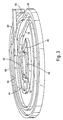
- planar coil 24 includes interior substantially semicircular loops 40, 42 and peripheral substantially circular segments 46 and 48 and an intermediate substantially circular segment 44. Loops 40 and 42 form half turns of coil 24 while each of loops 44, 46 and 48 forms almost a complete full turn; the full and half turns are connected in series with each other. All of segments 40, 42, 44, 46 and 48 are coaxial with central coil axis 50, coincident with the center axis of chamber 10. Opposite excitation terminals 52 and 54, in the center portion of coil 24, are respectively coupled by leads 48 and 56 to opposite terminals of r.f. source 26 via matching network 28 and one electrode of capacitor 80, the other electrode of which is grounded.
- Terminal 60 at the end of loop 40 opposite from terminal 52, is connected to end terminal 66 of outer loop segment 48 by conductive strap 64 which is located in a region slightly above the plane of coil 24 and does not touch any of the coil segments which run beneath it so the strap is electrically insulated from coil 24, except at terminals 60 and 66.
- Segment 48 has a second terminal 68 slightly less than 360° from terminal 66; terminal 68 is connected to terminal 70 of loop segment 46 via strap 72.
- Loop 46 having an angular extent of almost 360°, has a second end terminal 74 connected to terminal 76 of loop 44 via strap 78.
- Loop 44 having an angular extent of almost 360°, has a second end terminal 80 which is connected by strap 82 to terminal 62 at the end of segment 42 opposite from terminal 54.
- the voltage and current of coil 24 are distributed by selecting the value of capacitor 80 so the peak-to-peak r.f. current at coil terminal 54 is a minimum and equals the peak-to-peak r.f. current at coil terminal 52.
- the coil has opposite polarity maximum peak-to-peak r.f. voltages at terminals 52 and 54 and the coil maximum r.f. current occurs near conductive strap 72.
- the peripheral regions of coil 24 produce greater magnetic flux than the center region of the coil because the magnitude of the peak-to-peak r.f. currents is greater in the peripheral segment of the coil relative to the magnitudes of the peak-to-peak currents of the central segments.
- the maximum peak-to-peak r.f. current amplitude occurs in substantially circular loop segment 46.
- the amplitudes of the peak-to-peak r.f. currents in adjacent loop segments 44 and 48 and in loop segment 46 and the spacing of loop segments 44, 46 and 48 from each other are such that magnetic fluxes from these three loop segments are combined in space to provide a total magnetic flux density, just under window 19, having a maximum value over a relatively broad annular area.
- the annular area extends from between loop segments 46 and 48 to between intermediate segment 44 and interior segments 40 and 42.
- the total magnetic flux is also relatively constant as a function of angular coordinate ⁇ , representing the angle about the coil periphery relative to a reference angle that extends through the coil center line 50, e.g., the reference angle extends horizontally in Fig. 2 to the left of center line 50.
- a spatially averaged magnetic flux which is constant along a particular coordinate value ⁇ provides a plasma which is radially symmetric along ⁇ .
- the amplitudes of the peak-to-peak r.f. currents in the two substantially semicircular, equal radius segments 40 and 42 are significantly less than the amplitudes of the currents in the other segments.
- Segments 40 and 42 derive sufficient magnetic fluxes which are spatially averaged with the magnetic fluxes derived from the other segments 44, 46 and 48 so a substantially uniform plasma flux is generated at the level of the processed surface of workpiece 32 across the diameter of the chamber.
- the electrostatic (i.e., capacitive) coupling of the voltages to the plasma for different portions of planar coil 24 has an influence on the uniformity of the generated plasma flux.
- the capacitive coupling of these voltages to the plasma depends on the magnitude of the peak-to-peak voltages occurring in the coil segments, as well as the thickness and dielectric material of window 19 which separates the coil from the plasma.
- the influence of the capacitive currents produced by the r.f. voltages is minimized by causing the highest r.f. peak-to-peak voltages to occur at terminals 52 and 54.
- the geometry of coil 24 and proper selection of the value of capacitor 80 cause the highest r.f. peak-to-peak voltages to occur at terminals 52 and 54.
- planar coil 24 produces a substantially planar plasma having a relatively uniform flux completely across workpiece 32, frequently shaped as a disc. Regardless of shape, substrate 32 has exterior edge dimensions only somewhat less than the interior dimensions of plasma processor chamber 10.
- coil 24 supplies a strong torroidal magnetic field to gas and plasma in the interior of vacuum chamber 18, just beneath window 18.
- Coil 24 also supplies an r.f. electrostatic field to the gas and plasma in chamber 18.
- the torroidal magnetic field extends in a plane generally parallel to lower face 19 of window 18 and has an axis (where the magnetic field is zero) substantially coincident with center line 50 of coil 24.
- the strong magnetic field excites charge particles in the plasma to produce free electrons and positive ions.
- the strong magnetic field prevents substantial diffusion of the charge carries from the torroidal magnetic field to workpiece 32.
- the r.f. electrostatic field coil 24 couples to chamber 18 accelerates the charge particles toward workpiece 32.
- pulse source 27 turns off r.f. source 26 or causes the r.f. source to produce a low amplitude envelope the torroidal magnetic field collapses and the electrostatic field turns off. Consequently, the charge particles in the plasma are free to diffuse when source 26 derives a zero or low amplitude output.
- pulse source 27 turns off r.f. source 26 for a short enough period, e.g., 10 microseconds, to prevent extinction of the r.f. plasma.
- pulse source 21 turns off r.f. source 26 for a long enough period, e.g. 10 milliseconds, to assure extinction of the r.f. plasma.
- the unconfined free electrons and positive ions can easily diffuse away from the volume where the confining torroidal magnetic field subsists while r.f. source 26 is on and supplies a large amount of power, e.g., more than 1 kilowatt, to coil 24.
- the voltage that source 31 applies to workpiece holder 30 assists in attracting to workpiece 32 the unconfined free electrons and positive ions that can easily diffuse away from the torroidal volume.
- the unconfined electrons and positive ions that are attracted to workpiece 32 in combination with other factors cause the plasma density incident on workpiece 32 to be substantially uniform.
- Factors affecting the density of the plasma on workpiece 32 include the pressure within chamber 10 and the usually fixed geometric arrangement of chamber 10, coil 24, workpiece holder 30, and workpiece 32 and variable parameters which are (1) pressure in chamber 10, (2) flow rate and type of processing gas admitted to chamber 10 through port 20, (3) the material and size of workpiece 32, (4) spacing between adjacent pulses source 26 applies to coil 24, which pulse source 27 controls, and (5) peak and minimum amplitudes of the pulse source 26 supplies to coil 24.
- a high degree of plasma density uniformity on workpiece 32 has been achieved (as described infra) with a chamber having a wall 12 with an interior circular diameter of 35.56 cm (14 inches), a circular window 18 having a 37.33 cm (14.7 inch) diameter, a coil 24 with a 12 inch diameter, a circular workpiece holder with an 8 inch diameter having an upper face extending parallel to and spaced about 11.93 cm (4.7 inches) from bottom face 19 of window 18.
- Modulation of the envelope of the 13.56 MHz r.f. carrier derived by source 26 improves the uniformity of plasma flux, i.e., plasma density, across workpiece 32.
- Varying the envelope modulations adjusts the plasma processing conditions in order to obtain ion flux uniformity incident on workpiece 32 within a specified uniformity target. This ability to adjust ion flux uniformity for each processing condition provides better plasma processing results across a wider range of operating conditions than would be possible using a conventional inductively coupled plasma source without amplitude modulation of r.f. source 26 by pulse source 27.
- the ability of input device 31 and controller 27 to change the duty cycle of the r.f. source 26 derives enables at will control of the etch characteristics of workpiece 32 as a function of the radius of workpiece 32. For example if greater etching of peripheral workpiece regions is desired, input device 31 and controller 29 activate pulse source 27 to cause source 26 to produce a continuous wave, constant amplitude envelope. If maximum etch uniformity is desired input device 31 sets the duty cycle of source 26 at an intermediate value, as discussed infra . If greater etching of the workpiece center region is desired input device 31 and controller 29 cause pulse source 27 to activate r.f. source to produce low duty cycle (e.g., fifteen percent) r.f. output.
- coil 24 has an area substantially exceeding the workpiece area.
- pulse source 27 applied 35 percent duty cycle on and off 50kHz amplitude modulation to the 13.56 MHz carrier of r.f. source 26 so that source 26 produced 7 microsecond r.f. pulses spaced from each other by 13 microseconds, while the silicon poly wafer was etched by chlorine at a pressure of 0,7 Pa (5 milliTorr).
- the thickness of the wafer at different radial and circumferential positions on the wafer upper face exposed to the plasma was monitored after the etching operation to determine the amount of material etched from these different positions. Since the amount of material etched from each position correlates very closely to the plasma density at each position, the thickness measurements determine the plasma densities. The standard deviation ( ⁇ ) of these thickness measurements thus provide a measure of the plasma density uniformity incident on the workpiece exposed surface, so that high uniformity is associated with a low standard deviation and vice versa.
- etch standard deviation for the previously described experiment was 1.527 compared to an etch standard deviation of 2.037 for continuous wave (c.w.) operation of source 26 in a second experiment; all factors other than pulse modulation were identical in these two experiments.
- Similar experiments, under identical conditions except for duty cycle, indicate greater etch uniformity, for duty cycles of source 26 less than 85% than for c.w. operation of source 26 as indicated by the following Table. TABLE duty cycle (%) etch standard deviation ( ⁇ ) 100 (c.w.) 2.037 85 2.017 75 1.823 65 1.565 50 1.653 35 1.527 25 1.845 16 1.864
- the substantially reduced etch standard deviation for duty cycles between 16 percent and 75 percent implies substantially greater plasma density uniformity for pulsed (i.e., amplitude modulated) operation of source 26 than for c.w. operation of source 26.
- the 35 percent duty cycle in addition to having the greatest etch uniformity, had center and peripheral regions with lower amounts of etched material than an intermediate region between the center and peripheral regions. Hence for the 35 percent duty cycle the density of the plasma incident on the center of the wafer was less than the plasma density on the portion of the wafer surrounding the wafer center portion. This condition, known as center fast, is usually considered highly advantageous, particularly when accompanied by great plasma density uniformity.
- the twenty-five percent and sixteen percent duty cycles resulted in greater center etching than intermediate and peripheral etching.
- the eighty-five percent and seventy-five percent duty cycles resulted in greater peripheral etching than intermediate and center etching.
- varying the duty cycle enables tailoring of the etch rate as a function of radius.
Landscapes
- Engineering & Computer Science (AREA)
- Physics & Mathematics (AREA)
- Plasma & Fusion (AREA)
- Chemical & Material Sciences (AREA)
- Analytical Chemistry (AREA)
- General Physics & Mathematics (AREA)
- Condensed Matter Physics & Semiconductors (AREA)
- Manufacturing & Machinery (AREA)
- Computer Hardware Design (AREA)
- Microelectronics & Electronic Packaging (AREA)
- Power Engineering (AREA)
- Drying Of Semiconductors (AREA)
- Plasma Technology (AREA)
Applications Claiming Priority (3)
| Application Number | Priority Date | Filing Date | Title |
|---|---|---|---|
| US09/343,246 US6319355B1 (en) | 1999-06-30 | 1999-06-30 | Plasma processor with coil responsive to variable amplitude rf envelope |
| US343246 | 1999-06-30 | ||
| PCT/US2000/017088 WO2001001443A1 (en) | 1999-06-30 | 2000-06-22 | Plasma processor with coil responsive to variable amplitude rf envelope |
Publications (2)
| Publication Number | Publication Date |
|---|---|
| EP1190436A1 EP1190436A1 (en) | 2002-03-27 |
| EP1190436B1 true EP1190436B1 (en) | 2008-08-13 |
Family
ID=23345299
Family Applications (1)
| Application Number | Title | Priority Date | Filing Date |
|---|---|---|---|
| EP00946836A Expired - Lifetime EP1190436B1 (en) | 1999-06-30 | 2000-06-22 | Plasma processor with coil responsive to variable amplitude rf envelope |
Country Status (7)
| Country | Link |
|---|---|
| US (1) | US6319355B1 (enExample) |
| EP (1) | EP1190436B1 (enExample) |
| JP (1) | JP5031159B2 (enExample) |
| KR (1) | KR100748050B1 (enExample) |
| DE (1) | DE60039874D1 (enExample) |
| TW (1) | TW494707B (enExample) |
| WO (1) | WO2001001443A1 (enExample) |
Families Citing this family (35)
| Publication number | Priority date | Publication date | Assignee | Title |
|---|---|---|---|---|
| US6531029B1 (en) * | 2000-06-30 | 2003-03-11 | Lam Research Corporation | Vacuum plasma processor apparatus and method |
| US7096819B2 (en) * | 2001-03-30 | 2006-08-29 | Lam Research Corporation | Inductive plasma processor having coil with plural windings and method of controlling plasma density |
| US6583572B2 (en) * | 2001-03-30 | 2003-06-24 | Lam Research Corporation | Inductive plasma processor including current sensor for plasma excitation coil |
| US6597117B2 (en) * | 2001-11-30 | 2003-07-22 | Samsung Austin Semiconductor, L.P. | Plasma coil |
| US7169255B2 (en) * | 2002-02-15 | 2007-01-30 | Hitachi High-Technologies Corporation | Plasma processing apparatus |
| US6783629B2 (en) | 2002-03-11 | 2004-08-31 | Yuri Glukhoy | Plasma treatment apparatus with improved uniformity of treatment and method for improving uniformity of plasma treatment |
| US6700090B2 (en) * | 2002-04-26 | 2004-03-02 | Hitachi High-Technologies Corporation | Plasma processing method and plasma processing apparatus |
| US6905626B2 (en) * | 2002-07-24 | 2005-06-14 | Unaxis Usa Inc. | Notch-free etching of high aspect SOI structures using alternating deposition and etching and pulsed plasma |
| US7147759B2 (en) * | 2002-09-30 | 2006-12-12 | Zond, Inc. | High-power pulsed magnetron sputtering |
| KR100486724B1 (ko) * | 2002-10-15 | 2005-05-03 | 삼성전자주식회사 | 사행 코일 안테나를 구비한 유도결합 플라즈마 발생장치 |
| US6896773B2 (en) * | 2002-11-14 | 2005-05-24 | Zond, Inc. | High deposition rate sputtering |
| US20050103620A1 (en) * | 2003-11-19 | 2005-05-19 | Zond, Inc. | Plasma source with segmented magnetron cathode |
| US9771648B2 (en) * | 2004-08-13 | 2017-09-26 | Zond, Inc. | Method of ionized physical vapor deposition sputter coating high aspect-ratio structures |
| US9123508B2 (en) * | 2004-02-22 | 2015-09-01 | Zond, Llc | Apparatus and method for sputtering hard coatings |
| WO2006036846A1 (en) * | 2004-09-24 | 2006-04-06 | Zond, Inc. | Apparatus for generating high-current electrical discharges |
| US8192576B2 (en) * | 2006-09-20 | 2012-06-05 | Lam Research Corporation | Methods of and apparatus for measuring and controlling wafer potential in pulsed RF bias processing |
| US20080204795A1 (en) * | 2007-02-23 | 2008-08-28 | Samsung Electronics Co., Ltd. | Data transmission apparatus and method of controlling the same and method of processing data to be printed onto a printable medium |
| US20080230008A1 (en) * | 2007-03-21 | 2008-09-25 | Alexander Paterson | Plasma species and uniformity control through pulsed vhf operation |
| US20090004836A1 (en) * | 2007-06-29 | 2009-01-01 | Varian Semiconductor Equipment Associates, Inc. | Plasma doping with enhanced charge neutralization |
| US9123509B2 (en) | 2007-06-29 | 2015-09-01 | Varian Semiconductor Equipment Associates, Inc. | Techniques for plasma processing a substrate |
| US20090017229A1 (en) * | 2007-07-10 | 2009-01-15 | Varian Semiconductor Equipment Associates, Inc. | Processing System Platen having a Variable Thermal Conductivity Profile |
| US7927986B2 (en) * | 2008-07-22 | 2011-04-19 | Varian Semiconductor Equipment Associates, Inc. | Ion implantation with heavy halogenide compounds |
| US20100048018A1 (en) * | 2008-08-25 | 2010-02-25 | Varian Semiconductor Equipment Associates, Inc. | Doped Layers for Reducing Electromigration |
| JP5227245B2 (ja) * | 2009-04-28 | 2013-07-03 | 東京エレクトロン株式会社 | プラズマ処理装置 |
| US8659335B2 (en) * | 2009-06-25 | 2014-02-25 | Mks Instruments, Inc. | Method and system for controlling radio frequency power |
| JP5546921B2 (ja) * | 2010-03-26 | 2014-07-09 | 株式会社日立国際電気 | 基板処理装置及び半導体装置の製造方法 |
| US8828883B2 (en) * | 2010-08-24 | 2014-09-09 | Micron Technology, Inc. | Methods and apparatuses for energetic neutral flux generation for processing a substrate |
| US10157729B2 (en) | 2012-02-22 | 2018-12-18 | Lam Research Corporation | Soft pulsing |
| US20130256271A1 (en) * | 2012-04-03 | 2013-10-03 | Theodoros Panagopoulos | Methods and apparatuses for controlling plasma in a plasma processing chamber |
| US9460894B2 (en) | 2013-06-28 | 2016-10-04 | Lam Research Corporation | Controlling ion energy within a plasma chamber |
| US9502221B2 (en) * | 2013-07-26 | 2016-11-22 | Lam Research Corporation | Etch rate modeling and use thereof with multiple parameters for in-chamber and chamber-to-chamber matching |
| TWI501307B (zh) * | 2013-07-31 | 2015-09-21 | 盛美半導體設備(上海)有限公司 | Pulse electrochemical polishing method and device |
| US10573496B2 (en) * | 2014-12-09 | 2020-02-25 | Applied Materials, Inc. | Direct outlet toroidal plasma source |
| EP3088435A1 (de) | 2015-04-28 | 2016-11-02 | Sika Technology AG | Zweistufiges verfahren zur herstellung eines polyurethan-heissschmelzklebstoffs mit niedrigem gehalt an monomeren diisocyanaten und hoher anfangsfestigkeit |
| TW202209401A (zh) * | 2020-05-01 | 2022-03-01 | 美商得昇科技股份有限公司 | 用於表面處理製程之脈衝式感應耦合電漿的方法及設備 |
Citations (1)
| Publication number | Priority date | Publication date | Assignee | Title |
|---|---|---|---|---|
| WO1999007913A1 (en) * | 1997-08-07 | 1999-02-18 | Applied Materials, Inc. | Modulated power for ionized metal plasma deposition |
Family Cites Families (19)
| Publication number | Priority date | Publication date | Assignee | Title |
|---|---|---|---|---|
| GB2212974B (en) | 1987-11-25 | 1992-02-12 | Fuji Electric Co Ltd | Plasma processing apparatus |
| EP0395415B1 (en) | 1989-04-27 | 1995-03-15 | Fujitsu Limited | Apparatus for and method of processing a semiconductor device using microwave-generated plasma |
| US4948458A (en) | 1989-08-14 | 1990-08-14 | Lam Research Corporation | Method and apparatus for producing magnetically-coupled planar plasma |
| US5304279A (en) | 1990-08-10 | 1994-04-19 | International Business Machines Corporation | Radio frequency induction/multipole plasma processing tool |
| JPH08979B2 (ja) * | 1991-12-06 | 1996-01-10 | 日新電機株式会社 | プラズマcvd法及び装置 |
| US5226967A (en) | 1992-05-14 | 1993-07-13 | Lam Research Corporation | Plasma apparatus including dielectric window for inducing a uniform electric field in a plasma chamber |
| US5277751A (en) | 1992-06-18 | 1994-01-11 | Ogle John S | Method and apparatus for producing low pressure planar plasma using a coil with its axis parallel to the surface of a coupling window |
| KR100238627B1 (ko) | 1993-01-12 | 2000-01-15 | 히가시 데쓰로 | 플라즈마 처리장치 |
| US5401350A (en) | 1993-03-08 | 1995-03-28 | Lsi Logic Corporation | Coil configurations for improved uniformity in inductively coupled plasma systems |
| JP3202877B2 (ja) * | 1994-08-30 | 2001-08-27 | 東京エレクトロン株式会社 | プラズマアッシング装置 |
| JP3105403B2 (ja) | 1994-09-14 | 2000-10-30 | 松下電器産業株式会社 | プラズマ処理装置 |
| JP2845163B2 (ja) * | 1994-10-27 | 1999-01-13 | 日本電気株式会社 | プラズマ処理方法及びその装置 |
| US5731565A (en) * | 1995-07-27 | 1998-03-24 | Lam Research Corporation | Segmented coil for generating plasma in plasma processing equipment |
| JPH0982495A (ja) * | 1995-09-18 | 1997-03-28 | Toshiba Corp | プラズマ生成装置およびプラズマ生成方法 |
| CA2207154A1 (en) * | 1996-06-10 | 1997-12-10 | Lam Research Corporation | Inductively coupled source for deriving substantially uniform plasma flux |
| US5800619A (en) | 1996-06-10 | 1998-09-01 | Lam Research Corporation | Vacuum plasma processor having coil with minimum magnetic field in its center |
| US5759280A (en) | 1996-06-10 | 1998-06-02 | Lam Research Corporation | Inductively coupled source for deriving substantially uniform plasma flux |
| JP3220394B2 (ja) * | 1996-09-27 | 2001-10-22 | 東京エレクトロン株式会社 | プラズマ処理装置 |
| JP3559429B2 (ja) * | 1997-07-02 | 2004-09-02 | 松下電器産業株式会社 | プラズマ処理方法 |
-
1999
- 1999-06-30 US US09/343,246 patent/US6319355B1/en not_active Expired - Lifetime
-
2000
- 2000-06-22 EP EP00946836A patent/EP1190436B1/en not_active Expired - Lifetime
- 2000-06-22 JP JP2001506574A patent/JP5031159B2/ja not_active Expired - Lifetime
- 2000-06-22 KR KR1020017016487A patent/KR100748050B1/ko not_active Expired - Lifetime
- 2000-06-22 DE DE60039874T patent/DE60039874D1/de not_active Expired - Lifetime
- 2000-06-22 WO PCT/US2000/017088 patent/WO2001001443A1/en not_active Ceased
- 2000-07-13 TW TW089112870A patent/TW494707B/zh not_active IP Right Cessation
Patent Citations (1)
| Publication number | Priority date | Publication date | Assignee | Title |
|---|---|---|---|---|
| WO1999007913A1 (en) * | 1997-08-07 | 1999-02-18 | Applied Materials, Inc. | Modulated power for ionized metal plasma deposition |
Also Published As
| Publication number | Publication date |
|---|---|
| EP1190436A1 (en) | 2002-03-27 |
| KR20020031344A (ko) | 2002-05-01 |
| TW494707B (en) | 2002-07-11 |
| WO2001001443B1 (en) | 2001-02-08 |
| DE60039874D1 (de) | 2008-09-25 |
| KR100748050B1 (ko) | 2007-08-09 |
| JP5031159B2 (ja) | 2012-09-19 |
| WO2001001443A1 (en) | 2001-01-04 |
| JP2003503839A (ja) | 2003-01-28 |
| US6319355B1 (en) | 2001-11-20 |
Similar Documents
| Publication | Publication Date | Title |
|---|---|---|
| EP1190436B1 (en) | Plasma processor with coil responsive to variable amplitude rf envelope | |
| US20220216036A1 (en) | Control method and plasma processing apparatus | |
| US6451161B1 (en) | Method and apparatus for generating high-density uniform plasma | |
| JP3739137B2 (ja) | プラズマ発生装置及びこのプラズマ発生装置を使用した表面処理装置 | |
| CN100565775C (zh) | 具有多个绕组线圈的感应等离子处理器和控制等离子浓度的方法 | |
| US5607542A (en) | Inductively enhanced reactive ion etching | |
| KR100777151B1 (ko) | 하이브리드형 플라즈마 반응장치 | |
| US4333814A (en) | Methods and apparatus for improving an RF excited reactive gas plasma | |
| US5759280A (en) | Inductively coupled source for deriving substantially uniform plasma flux | |
| JP6548748B2 (ja) | プラズマ処理方法およびプラズマ処理装置 | |
| JP3381916B2 (ja) | 低周波誘導型高周波プラズマ反応装置 | |
| US6646385B2 (en) | Plasma excitation coil | |
| KR100188076B1 (ko) | 자기 결합성 플래너 플라즈마 형성 방법 및 장치 | |
| US7426900B2 (en) | Integrated electrostatic inductive coupling for plasma processing | |
| US6022460A (en) | Enhanced inductively coupled plasma reactor | |
| US20030132198A1 (en) | Method and apparatus for treating surface of semiconductor | |
| CN111183504B (zh) | 制造过程中的超局部和等离子体均匀性控制 | |
| KR0170387B1 (ko) | 고주파 반도체 웨이퍼 가공장치 및 방법 | |
| KR102867184B1 (ko) | 플라즈마 반응기 내의 전극들에 대한 이온 에너지 제어 | |
| EP1300057B1 (en) | Coil for vacuum plasma processor | |
| JP3563054B2 (ja) | プラズマ処理装置および方法 | |
| US6462483B1 (en) | Induction plasma processing chamber | |
| JP2000164394A (ja) | プラズマ処理装置 | |
| JPH0982494A (ja) | プラズマ処理装置およびプラズマ処理方法 | |
| TW202425046A (zh) | 處理腔室中的腔室阻抗管理 |
Legal Events
| Date | Code | Title | Description |
|---|---|---|---|
| PUAI | Public reference made under article 153(3) epc to a published international application that has entered the european phase |
Free format text: ORIGINAL CODE: 0009012 |
|
| 17P | Request for examination filed |
Effective date: 20011219 |
|
| AK | Designated contracting states |
Kind code of ref document: A1 Designated state(s): AT BE CH CY DE DK ES FI FR GB GR IE IT LI LU MC NL PT SE |
|
| RBV | Designated contracting states (corrected) |
Designated state(s): DE ES FR GB IE IT |
|
| 17Q | First examination report despatched |
Effective date: 20061005 |
|
| 17Q | First examination report despatched |
Effective date: 20061005 |
|
| 17Q | First examination report despatched |
Effective date: 20061005 |
|
| GRAP | Despatch of communication of intention to grant a patent |
Free format text: ORIGINAL CODE: EPIDOSNIGR1 |
|
| GRAS | Grant fee paid |
Free format text: ORIGINAL CODE: EPIDOSNIGR3 |
|
| GRAA | (expected) grant |
Free format text: ORIGINAL CODE: 0009210 |
|
| AK | Designated contracting states |
Kind code of ref document: B1 Designated state(s): DE ES FR GB IE IT |
|
| REG | Reference to a national code |
Ref country code: GB Ref legal event code: FG4D |
|
| REG | Reference to a national code |
Ref country code: IE Ref legal event code: FG4D |
|
| REF | Corresponds to: |
Ref document number: 60039874 Country of ref document: DE Date of ref document: 20080925 Kind code of ref document: P |
|
| PG25 | Lapsed in a contracting state [announced via postgrant information from national office to epo] |
Ref country code: ES Free format text: LAPSE BECAUSE OF FAILURE TO SUBMIT A TRANSLATION OF THE DESCRIPTION OR TO PAY THE FEE WITHIN THE PRESCRIBED TIME-LIMIT Effective date: 20081124 |
|
| PLBE | No opposition filed within time limit |
Free format text: ORIGINAL CODE: 0009261 |
|
| STAA | Information on the status of an ep patent application or granted ep patent |
Free format text: STATUS: NO OPPOSITION FILED WITHIN TIME LIMIT |
|
| 26N | No opposition filed |
Effective date: 20090514 |
|
| PG25 | Lapsed in a contracting state [announced via postgrant information from national office to epo] |
Ref country code: IT Free format text: LAPSE BECAUSE OF FAILURE TO SUBMIT A TRANSLATION OF THE DESCRIPTION OR TO PAY THE FEE WITHIN THE PRESCRIBED TIME-LIMIT Effective date: 20080813 |
|
| PG25 | Lapsed in a contracting state [announced via postgrant information from national office to epo] |
Ref country code: IE Free format text: LAPSE BECAUSE OF NON-PAYMENT OF DUE FEES Effective date: 20090622 |
|
| PGFP | Annual fee paid to national office [announced via postgrant information from national office to epo] |
Ref country code: GB Payment date: 20120625 Year of fee payment: 13 |
|
| GBPC | Gb: european patent ceased through non-payment of renewal fee |
Effective date: 20130622 |
|
| PG25 | Lapsed in a contracting state [announced via postgrant information from national office to epo] |
Ref country code: GB Free format text: LAPSE BECAUSE OF NON-PAYMENT OF DUE FEES Effective date: 20130622 |
|
| REG | Reference to a national code |
Ref country code: FR Ref legal event code: PLFP Year of fee payment: 16 |
|
| REG | Reference to a national code |
Ref country code: FR Ref legal event code: PLFP Year of fee payment: 17 |
|
| REG | Reference to a national code |
Ref country code: FR Ref legal event code: PLFP Year of fee payment: 18 |
|
| REG | Reference to a national code |
Ref country code: FR Ref legal event code: PLFP Year of fee payment: 19 |
|
| PGFP | Annual fee paid to national office [announced via postgrant information from national office to epo] |
Ref country code: FR Payment date: 20190625 Year of fee payment: 20 |
|
| PGFP | Annual fee paid to national office [announced via postgrant information from national office to epo] |
Ref country code: DE Payment date: 20190627 Year of fee payment: 20 |
|
| REG | Reference to a national code |
Ref country code: DE Ref legal event code: R071 Ref document number: 60039874 Country of ref document: DE |