EP1189142A2 - Verfahren und Vorrichtung zum Datenaustausch zwischen Speicher- und Logikbausteinen - Google Patents
Verfahren und Vorrichtung zum Datenaustausch zwischen Speicher- und Logikbausteinen Download PDFInfo
- Publication number
- EP1189142A2 EP1189142A2 EP01118364A EP01118364A EP1189142A2 EP 1189142 A2 EP1189142 A2 EP 1189142A2 EP 01118364 A EP01118364 A EP 01118364A EP 01118364 A EP01118364 A EP 01118364A EP 1189142 A2 EP1189142 A2 EP 1189142A2
- Authority
- EP
- European Patent Office
- Prior art keywords
- signal
- converter
- analog
- calibration
- analog signal
- Prior art date
- Legal status (The legal status is an assumption and is not a legal conclusion. Google has not performed a legal analysis and makes no representation as to the accuracy of the status listed.)
- Ceased
Links
- 238000000034 method Methods 0.000 title claims abstract description 26
- 230000015654 memory Effects 0.000 title claims abstract description 14
- 230000005540 biological transmission Effects 0.000 claims abstract description 16
- 239000003990 capacitor Substances 0.000 claims description 16
- 238000012546 transfer Methods 0.000 description 7
- 238000006243 chemical reaction Methods 0.000 description 4
- 238000004519 manufacturing process Methods 0.000 description 2
- 238000012937 correction Methods 0.000 description 1
- 238000013016 damping Methods 0.000 description 1
- 230000007423 decrease Effects 0.000 description 1
- 238000011161 development Methods 0.000 description 1
- 238000010586 diagram Methods 0.000 description 1
- 238000007599 discharging Methods 0.000 description 1
- 238000011156 evaluation Methods 0.000 description 1
- 238000005259 measurement Methods 0.000 description 1
- 230000000704 physical effect Effects 0.000 description 1
- 230000008054 signal transmission Effects 0.000 description 1
- 238000012360 testing method Methods 0.000 description 1
Images


Classifications
-
- H—ELECTRICITY
- H03—ELECTRONIC CIRCUITRY
- H03M—CODING; DECODING; CODE CONVERSION IN GENERAL
- H03M1/00—Analogue/digital conversion; Digital/analogue conversion
- H03M1/66—Digital/analogue converters
- H03M1/74—Simultaneous conversion
- H03M1/742—Simultaneous conversion using current sources as quantisation value generators
- H03M1/745—Simultaneous conversion using current sources as quantisation value generators with weighted currents
-
- H—ELECTRICITY
- H03—ELECTRONIC CIRCUITRY
- H03M—CODING; DECODING; CODE CONVERSION IN GENERAL
- H03M1/00—Analogue/digital conversion; Digital/analogue conversion
- H03M1/10—Calibration or testing
- H03M1/1009—Calibration
- H03M1/1014—Calibration at one point of the transfer characteristic, i.e. by adjusting a single reference value, e.g. bias or gain error
-
- H—ELECTRICITY
- H04—ELECTRIC COMMUNICATION TECHNIQUE
- H04L—TRANSMISSION OF DIGITAL INFORMATION, e.g. TELEGRAPHIC COMMUNICATION
- H04L25/00—Baseband systems
- H04L25/38—Synchronous or start-stop systems, e.g. for Baudot code
- H04L25/40—Transmitting circuits; Receiving circuits
- H04L25/49—Transmitting circuits; Receiving circuits using code conversion at the transmitter; using predistortion; using insertion of idle bits for obtaining a desired frequency spectrum; using three or more amplitude levels ; Baseband coding techniques specific to data transmission systems
- H04L25/4917—Transmitting circuits; Receiving circuits using code conversion at the transmitter; using predistortion; using insertion of idle bits for obtaining a desired frequency spectrum; using three or more amplitude levels ; Baseband coding techniques specific to data transmission systems using multilevel codes
-
- H—ELECTRICITY
- H04—ELECTRIC COMMUNICATION TECHNIQUE
- H04L—TRANSMISSION OF DIGITAL INFORMATION, e.g. TELEGRAPHIC COMMUNICATION
- H04L5/00—Arrangements affording multiple use of the transmission path
- H04L5/02—Channels characterised by the type of signal
- H04L5/04—Channels characterised by the type of signal the signals being represented by different amplitudes or polarities, e.g. quadriplex
-
- H—ELECTRICITY
- H03—ELECTRONIC CIRCUITRY
- H03M—CODING; DECODING; CODE CONVERSION IN GENERAL
- H03M1/00—Analogue/digital conversion; Digital/analogue conversion
- H03M1/12—Analogue/digital converters
- H03M1/34—Analogue value compared with reference values
- H03M1/38—Analogue value compared with reference values sequentially only, e.g. successive approximation type
- H03M1/46—Analogue value compared with reference values sequentially only, e.g. successive approximation type with digital/analogue converter for supplying reference values to converter
-
- H—ELECTRICITY
- H04—ELECTRIC COMMUNICATION TECHNIQUE
- H04L—TRANSMISSION OF DIGITAL INFORMATION, e.g. TELEGRAPHIC COMMUNICATION
- H04L25/00—Baseband systems
- H04L25/02—Details ; arrangements for supplying electrical power along data transmission lines
- H04L25/0264—Arrangements for coupling to transmission lines
- H04L25/028—Arrangements specific to the transmitter end
Definitions
- the invention relates in particular to a method and a device for data exchange between memory and logic modules.
- the transfer rate of (memory) information from the memory chip to processor and vice versa is currently a Main factor in limiting computer performance. While today's processors have frequencies of 800 MHz and the corresponding transmission rates, the frequencies lie for data exchange between processor / controller and Storage currently at 100 to maximum for technical reasons 133 MHz. Therefore new circuits and / or are urgently needed Procedures sought to understand the importance of this limiting factor weaken and the high processor frequencies also in to use the application.
- the former in turn leads to a linear increase with frequency Transfer rate, the latter to an increase by Factor 2.
- the "real" frequency on the data pins is at constantly changing data also twice as large.
- the process according to the invention requires a D / A converter on the respective transmitter side multiple bits (digital states) for transmission over one Converted transmission path (bus system) into an analog state (a current or a voltage).
- this implementation must be reversed so that on the receiving end through analog / digital conversion from the received Analog signal received digital signal is identical to the one sent Digital signal.
- Suitable digital / analog converters for the stated purpose known.
- This principle of the successively approximating A / D converter has the advantage that it is relatively easy to calibrate.
- the method and the device presented here can be used for the above procedure (A) changes the number of pins required reduce a factor k (integer) that corresponds to the number of in an analog state encoded bits of the digital signal equivalent.
- a factor k integer
- Signal transmission rate can be increased by the factor k or at constant transmission rate, the frequency by a factor of k be reduced.
- the method according to the invention allows for an increased Bandwidth, multiple blocks use the same bus line can, as previously with SDRAM, EDORAMs, Direct Rambus, by all blocks not read at a time have their outputs switch to "High Impedance".
- the level of the bus line is then driven solely by the one driven by the active block Level determined. That means that the system to existing bus systems is compatible.
- the decoding of an analog value on the receiver side requires some time, it is advantageous to use multiple decoders, i. H. A / D converter, per pin on a chip, to use and To multiplex input signals in time. This would allow a further increase in bandwidth as long as not a limitation of the physical properties of the bus system bring with it. To do this, the analog Input signal can be temporarily stored, e.g. B. in Capacitors.
- one assigns on the receiver side using, successively approximating analog / digital converter a calibration device on that a simple calibration based on at least one input signal at the same time avoiding a discretization error.
- inventive method and the not designed to perform the same device the data transfer between memory and logic modules limited but can be used with advantage anywhere be where previously important in the transmission of digital data There were restrictions on the transmission rate.
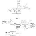
- FIG. 1 shows a simple implementation of a multilevel driver forming a D / A converter, in which a plurality of driver branches connected in parallel each have at least one n-channel FET T1, T2 and T3 for 3-bit digits Bit1, Bit2 and Bit3 which draw current from a termination voltage V term via a resistor R term .
- the saturation currents of these branches behave like powers of two.
- the driver currents Bit1: Bit2: Bit3 4: 2: 1.
- the output signal AUS is a current (voltage swing) which corresponds to a digital value with n bit positions. How many bits can actually be encoded depends on the measurement resolution when decoding on the receiver side and z. B. on the size of possible interference signals on the bus, as they are caused by crosstalk of other lines to the level to be evaluated.
- the by a D / A converter circuit z. B. generated according to FIG. 1 Analog value is via a transmission or bus line 10 sent to the recipient side.
- a / D converter On the receiver side there is an A / D converter which, for. B. an analog / digital converter 2 as shown in FIG. 2 can be.
- the A / D converter shown in Fig. 2 has a capacitor C which is charged to a (buffered) copy of the voltage swing from the transmission line 10 (the analog driver signal).
- the capacitor C preferably has a large capacitance with a correspondingly large charging current in order to obtain a large signal, namely the amount of charge stored.
- the capacitor C is separated from the input by a switch S1 and is discharged from a constant current source I const after a switch S2 has been closed.
- the digital value is created by a running counter Z, clocked at a fixed clock frequency, which has as many bits as the digital signal and which measures the time for the capacitor to discharge.
- the counter Z begins to count when the switch S2 is closed and stops when a comparator CMP generates an output signal "OFF".
- the digital value that can be derived from the counter Z corresponds to the amount of charge on the capacitor C and is proportional to the voltage swing of the analog input signal, "ANALOG-ON", when the capacitance is fixed.
- the capacitor C can only be used for calibration once fully discharged and one counter larger Number of bits than are actually to be decoded. This must be at least twice the value when fully discharged, i.e. H. one full bit more of the desired counter reading "all bits on” have and run accordingly fast. Then this can Counter value in operation arithmetically or in terms of circuitry the desired value "all bits on” or correspondingly smaller Values are implemented with smaller input values.
- the analog input voltage V bus from the bus line system 10 arises at a terminating resistor R term as a voltage drop against a voltage V term .
- the voltage V bus on the bus line 10 is applied via a voltage follower T u for a certain time (order of magnitude ns) by closing a switch S1 to a capacitor C which serves as a (short-term) memory for this voltage. Then the switch S1 is opened so that the capacitor C is decoupled from the input of the circuit, and by closing a switch S2 the capacitor C is connected to a first input of a differential amplifier CMP operating as a comparator.
- step D1 the transistor T2 switched on. A voltage drop occurs across R int , V decode is present at the comparator CMP.
- step D2 it is queried whether V decode is greater than V bus . In the affirmative, the higher-order bit 2 remains set and the transistor T2 remains switched on. Then transistor T1 is switched on. If V decode is not greater than V bus , transistor T2 is switched off in step D3 and transistor T1 is switched on (step D4).
- step D5 If V decode is still greater than V bus (step D5), the maximum value is decoded and the routine is ended in step D7. In this case, the decoded value must be "1 1". If it is determined in decision step D5 that V decode is not greater than V bus , T1 is switched off. Then the decoded state in step D7 is either the state "1 0" or "0 0", depending on the result determined in step D2.
- this circuit has a fundamental problem when used to decode an analog voltage that was itself generated by a 2-bit D / A converter: when the voltage swing V bus caused by the setting of a bit (e.g. Bit 1) arises in the original signal, is exactly identical to the one that arises from switching one of the transistors in the A / D converter (e.g. T1), the differential amplifier CMP cannot decide whether the corresponding bit in the decoded Signal or not.
- a bit e.g. Bit 1
- the additional "overdrive" transistor T0 establishes the uniqueness of the decoded (2 bit) digital signal with the (2 bit) digital signal converted on the transmitter side into an analog signal V bus .
- the calibration is carried out in a special calibration cycle.
- the most significant bit is set on the transmitter side and switches S3 and S4 are set to the "calibration" position on the receiver side and transistor 2 and additionally the "overdrive” transistor T0 are switched on with the control block 6.
- the output of the differential amplifier CMP acts on a register 5, with which the value of the gate voltage V gate of the transistors T2 and T1 (via the transfer gates 7 and 8) and of the "overdrive” transistor T0 can be adjusted in fine steps. If V bus, 2 is larger than V decode , the register value and thus V gate should be increased. If V bus, 2 is less than V decode , the register value and thus V gate should be reduced.
- the transistors T1 and T2 are therefore not switched on at a full high level on the gate, but rather by means of a gate voltage which can be adjusted by the voltage V gate of the register 5.
- the on / off signal is only switched to a transfer gate 7, 8, which connects the transistor gates to the adjustable voltage V gate .
- the voltage V gate of the register 5 is adjusted until a certain threshold for the amount of the output voltage of the differential amplifier CMP is undershot, ie V bus and V decode are almost the same.
- the output voltage of the amplifier CMP integrated over a certain time can also be used for a reliable evaluation. However, this makes the calibration process more time-consuming.
- the "overdrive transistor T 0” ensures that a little more current has to be drawn on the receiver side, ie on the side of the A / D converter 4, than by T2 alone, so that the differential amplifier CMP has a vanishing output signal , namely the current contribution made by the "overdrive” transistor T0. If the "overdrive” transistor T0 is always left switched off in normal decoding mode, whenever a bit was set in the original signal before the D / A conversion in the transmitter, this is also in the A / D described and shown in FIG. 4 Converter 4 set, which is apparent from the above description of the decoding.
- the calibration can be refined / checked if you are in the original signal not only sets the most significant bit, but the process for different bits or bit combinations repeated. However, this extends the calibration cycle.
- the calibration on the receiver side influences a possible damping between the transmitter side and the receiver side switched off. This is because correct decoding is also carried out on the receiver side if the analog signal transmitted by the transmitter on the receiver side arrives only weakened as an input signal.
- the Calibration only uses the linearity of the input signal on the receiver side to the transmitted signal and not an identity of absolute values of that emitted by the transmitter Transmission signal with the signal arriving at the receiver.
Landscapes
- Engineering & Computer Science (AREA)
- Signal Processing (AREA)
- Computer Networks & Wireless Communication (AREA)
- Theoretical Computer Science (AREA)
- Physics & Mathematics (AREA)
- Spectroscopy & Molecular Physics (AREA)
- Analogue/Digital Conversion (AREA)
Abstract
Description
- Fig. 1
- zeigt schematisch ein Ausführungsbeispiel eines 3-Bit-D/A-Wandlers zur Erzeugung eines analogen Ausgangssignals.
- Fig. 2
- zeigt schematisch ein erstes Ausführungsbeispiel eines einfachen A/D-Wandlers zur Umsetzung eines analogen Eingangssignals in ein digitales Signal.
- Fig. 3
- zeigt ein erstes Ausführungsbeispiel eines nach dem Prinzip der sukzessiven Approximation arbeitenden A/D-Wandlers zur Umsetzung eines Analogsignals in ein Digitalsignal mit zwei Bitstellen.
- Fig. 4
- zeigt ein weiteres Ausführungsbeispiel eines nach dem Prinzip der sukzessiven Approximation arbeitenden 2-Bit-A/D-Wandlers mit einem zusätzlichen Overdrive-Transistor zur eindeutigen Dekodierung eines Analogsignals und einer zusätzlichen Kalibrierschaltung, und
- Fig. 5
- zeigt ein Flussdiagramm zur Analog-/Digital-Wandlung in einen 2-Bit-Wert durch sukzessive Approximation eines A/D-Wandlers gemäß Fig. 3.
Claims (12)
- Verfahren zum Datenaustausch, insbesondere zwischen Speicher- und Logikbausteinen,
dadurch gekennzeichnet,dass auf der Senderseite ein mehrstelliges Digitalsignal in ein entsprechendes Analogsignal umgesetzt,dass dieses Analogsignal übertragen unddass auf der Empfängerseite das übertragene Analogsignal wieder in ein mit dem mehrstelligen Digitalsignal der Senderseite identisches mehrstelliges Digitalsignal umgesetzt wird. - Verfahren nach Anspruch 1,
dadurch gekennzeichnet, dass auf der Empfängerseite mehrere empfangene Analogsignale gespeichert und im Zeitmultiplex verarbeitet werden. - Verfahren nach Anspruch 1 oder 2,
dadurch gekennzeichnet, dass auf der Empfängerseite eine Kalibrierung des aus dem empfangenen Analogsignal umgesetzten Digitalsignals, bezogen auf wenigstens einen Signalwert, durchgeführt wird. - Verfahren nach Anspruch 3,
dadurch gekennzeichnet, dass der zu kalibrierende Signalwert der maximale Signalwert ist. - Verfahren nach Anspruch 3 oder 4,
dadurch gekennzeichnet, dass durch die Kalibrierung auf der Empfängerseite Einflüsse einer Dämpfung zwischen Senderseite und Empfängerseite ausgeschaltet werden. - Verfahren nach einem der Ansprüche 3 bis 5,
dadurch gekennzeichnet, dass die Kalibrierung auf der Empfängerseite die Linearität des in die Empfängerseite eingespeisten Analogsignals nutzt. - Vorrichtung zum Datenaustausch, insbesondere zwischen Speicher- und Logikbausteinen zur Durchführung des Verfahrens nach einem der Ansprüche 1 bis 6,
dadurch gekennzeichnet,dass auf der Senderseite ein Digital-/Analog(D/A)-Wandler (1) vorgesehen ist, der mehrere Bitstellen eines Digitalsignals in ein entsprechendes Analogsignal umwandelt,dass eine Übertragungsstrecke (10) zur Übertragung des Analogsignals eingerichtet ist, unddass auf der Empfängerseite ein Analog-/Digital(A/D)-Wandler (2; 3; 4) vorgesehen ist, der das übertragene und empfangene Analogsignal wieder in ein mit dem mehrstelligen Digitalsignal auf der Senderseite identisches mehrstelliges Digitalsignal zurückwandelt. - Vorrichtung nach Anspruch 7,
dadurch gekennzeichnet, dass ein A/D-Wandler (2) eingesetzt ist, der den jeweiligen Spannungszustand des empfangenen Analogsignals kurzzeitig in einen Kondensator (C) speichert, der anschließend über eine Konstantstromquelle (Iconst) entladen wird, und
die Dekodierung durch einen mitlaufenden Zähler (Z) so durchgeführt wird, dass dieser die für die Entladung des Kondensators (C) benötigte Zeit misst. - Vorrichtung nach Anspruch 7,
dadurch gekennzeichnet, dass ein A/D-Wandler (3; 4) eingesetzt ist, der nach dem Prinzip der sukzessiven Approximation arbeitet und einen internen D/A-Wandler (T1, T2, T0) aufweist, dessen analoger Ausgangswert (Vdecode) durch einen Vergleicher (CMP) mit dem empfangenen zu dekodierenden analogen Signal (Vbus) verglichen und solange verstellt wird, bis das entstehende Analogsignal (Vdecode) und das vom Sender gesendete Analogsignal (Vbus) gleich groß sind. - Vorrichtung nach Anspruch 9,
dadurch gekennzeichnet, dass der interne D/A-Wandler des A/D-Wandlers (4) eine Kalibriervorrichtung (5, T0, S3, S4) aufweist, die eine Kalibrierung des zum Vergleich erzeugten Digitalsignals für wenigstens einen Wert des analogen Eingangssignals (Vbus) durchführt. - Vorrichtung nach Anspruch 10,
dadurch gekennzeichnet, dass die Kalibriervorrichtung in dem D/A-Wandler des sukzessiv approximierenden A/D-Wandlers (4) einen zusätzlichen "Overdrive"-Transistor (T0), dessen Sättigungsstrom genau die Hälfte des Sättigungsstroms des der niedrigstwertigen Bitstelle des umgesetzten Digitalsignals entsprechenden Transistors (T1) ist und Mittel (5, S3, S4, 7, 8) aufweist, mit denen in Abhängigkeit von der Größe eines von der Senderseite gesendeten Kalibriersignals die durch die Transistoren (T0, T1, T2) des D/A-Wandlers des sukzessiv approximierenden A/D-Wandlers (4) fließenden Ströme in feinen Stufen solange verstellt werden, bis das als Kalibriersignal empfangene Analogsignal (Vbus) und das vom D/A-Wandler des sukzessiv approximierenden A/D-Wandlers (4) erzeugte Vergleichskalibriersignal nahezu identisch sind. - Analog-/Digital-Wandler nach dem Prinzip der sukzessiven Approximation mit einer Kalibriervorrichtung nach einem der Ansprüche 10 oder 11.
Applications Claiming Priority (2)
| Application Number | Priority Date | Filing Date | Title |
|---|---|---|---|
| DE10041380 | 2000-08-23 | ||
| DE2000141380 DE10041380A1 (de) | 2000-08-23 | 2000-08-23 | Verfahren und Vorrichtung zum Datenaustausch zwischen Speicher- und Logikbausteinen |
Publications (2)
| Publication Number | Publication Date |
|---|---|
| EP1189142A2 true EP1189142A2 (de) | 2002-03-20 |
| EP1189142A3 EP1189142A3 (de) | 2006-05-17 |
Family
ID=7653513
Family Applications (1)
| Application Number | Title | Priority Date | Filing Date |
|---|---|---|---|
| EP01118364A Ceased EP1189142A3 (de) | 2000-08-23 | 2001-07-27 | Verfahren und Vorrichtung zum Datenaustausch zwischen Speicher- und Logikbausteinen |
Country Status (4)
| Country | Link |
|---|---|
| US (1) | US6545625B2 (de) |
| EP (1) | EP1189142A3 (de) |
| DE (1) | DE10066029B4 (de) |
| TW (1) | TW531967B (de) |
Families Citing this family (9)
| Publication number | Priority date | Publication date | Assignee | Title |
|---|---|---|---|---|
| US7224300B2 (en) * | 2001-11-30 | 2007-05-29 | Second Sight Medical Products, Inc. | Floating gate digital-to-analog converter |
| US20040223462A1 (en) * | 2003-05-09 | 2004-11-11 | International Business Machines Corporation | Auto negotiate extension for ethernet infrastructure |
| EP1655842A1 (de) * | 2004-11-03 | 2006-05-10 | Dialog Semiconductor GmbH | Analog-Digital-Wandler mit domino-asynchroner schrittweiser Annäherung |
| US8174603B2 (en) * | 2008-05-01 | 2012-05-08 | Alexander Krymski | Image sensors and methods with antiblooming channels and two side driving of control signals |
| US8354918B2 (en) * | 2008-08-29 | 2013-01-15 | Boyer Stephen W | Light, sound, and motion receiver devices |
| US8316245B1 (en) * | 2008-12-11 | 2012-11-20 | Integrated Device Technology, Inc. | Method and apparatus for fail-safe start-up circuit for subthreshold current sources |
| US10756857B2 (en) * | 2013-01-25 | 2020-08-25 | Infineon Technologies Ag | Method, apparatus and computer program for digital transmission of messages |
| CN104348485B (zh) * | 2013-08-06 | 2017-09-15 | 博通集成电路(上海)有限公司 | 模数转换器和将模拟信号转换为数字信号的方法 |
| WO2017005748A1 (en) * | 2015-07-07 | 2017-01-12 | Infineon Technologies Ag | Built-in self-test for adc |
Citations (1)
| Publication number | Priority date | Publication date | Assignee | Title |
|---|---|---|---|---|
| JPS6414631A (en) * | 1987-07-08 | 1989-01-18 | Hitachi Ltd | Analog bus connecting system |
Family Cites Families (9)
| Publication number | Priority date | Publication date | Assignee | Title |
|---|---|---|---|---|
| DE2732603C3 (de) | 1977-07-19 | 1981-08-27 | Siemens AG, 1000 Berlin und 8000 München | Schaltungsanordnung zur Umsetzung von Analog-Signalen in Digital-Signale und umgekehrt von Digital-Signalen in Analog-Signale |
| US4821321A (en) * | 1981-12-31 | 1989-04-11 | The United States Of America As Represented By The Secretary Of The Army | Automatic secure transmission and reception of pictorial information |
| US4958344A (en) * | 1985-12-18 | 1990-09-18 | Advanced Micro Devices, Inc. | System for transmitting and receiving asynchronous nonhomogeneous variable width parallel data over a synchronous high speed serial transmission media |
| US5115450A (en) * | 1989-07-06 | 1992-05-19 | Advanced Micro Devices, Inc. | High speed digital to analog to digital communication system |
| GB9014679D0 (en) * | 1990-07-02 | 1990-08-22 | Sarnoff David Res Center | Sequential successive approximation a/d converter |
| FR2664765B1 (fr) * | 1990-07-11 | 2003-05-16 | Bull Sa | Dispositif de serialisation et de deserialisation de donnees et systeme de transmission numerique de donnees en serie en resultant. |
| US5055847A (en) * | 1991-02-19 | 1991-10-08 | Motorola, Inc. | Differential sensing current-steering analog-to-digital converter |
| US5153592A (en) * | 1991-04-30 | 1992-10-06 | Texas Instruments Incorporated | 16 bit error-correcting digital-to-analog converter |
| US5946355A (en) * | 1997-03-21 | 1999-08-31 | Tektronix, Inc. | Serial-digital receiver |
-
2000
- 2000-08-23 DE DE10066029A patent/DE10066029B4/de not_active Expired - Fee Related
-
2001
- 2001-07-27 EP EP01118364A patent/EP1189142A3/de not_active Ceased
- 2001-08-21 TW TW090120475A patent/TW531967B/zh not_active IP Right Cessation
- 2001-08-23 US US09/935,503 patent/US6545625B2/en not_active Expired - Lifetime
Patent Citations (1)
| Publication number | Priority date | Publication date | Assignee | Title |
|---|---|---|---|---|
| JPS6414631A (en) * | 1987-07-08 | 1989-01-18 | Hitachi Ltd | Analog bus connecting system |
Non-Patent Citations (1)
| Title |
|---|
| JOHNS D. ET AL: "ANALOG INTEGRATED CIRCUIT DESIGN", 1997, JOHN WILEY & SONS, INC., NEW YORK US * |
Also Published As
| Publication number | Publication date |
|---|---|
| EP1189142A3 (de) | 2006-05-17 |
| DE10066029B4 (de) | 2005-11-10 |
| TW531967B (en) | 2003-05-11 |
| DE10066029A1 (de) | 2002-05-08 |
| US20020024457A1 (en) | 2002-02-28 |
| US6545625B2 (en) | 2003-04-08 |
Similar Documents
| Publication | Publication Date | Title |
|---|---|---|
| DE102004041023B4 (de) | Integrierte Schaltung und zugehöriger Halbleiterspeicherbaustein | |
| DE69120606T2 (de) | Selbsteinstellender Treiber für Impedanzanpassung | |
| DE10084797B4 (de) | Schaltung und Verfahren zum Erfassen von mehreren Gleichheiten in Assoziativspeichern | |
| DE602004008456T2 (de) | Integrierte ladungsleseschaltung für resistive speicher | |
| DE68920153T2 (de) | Hochdichte halbleiterschaltung fuer analogsignalspeicherungs- und abspielsystem. | |
| DE69813356T2 (de) | Halbleiterschaltung für Aufnahme und Wiedergabe analoger Signale und Mitteilungsverwaltungssystem | |
| DE602004004002T2 (de) | Verfahren und Speichersystem basierend auf dualem data strobe mode and einfachem data strobe mode mit Dateninversion | |
| EP0104442B1 (de) | Monolithisch integrierte digitale Halbleiterschaltung | |
| DE2340547B2 (de) | Schaltungsanordnung zum testen logischer schaltungen | |
| DE102007039604A1 (de) | Kalibrierungsschaltung, damit ausgestattete Halbleitervorrichtung und Verfahren zur Einstellung der Ausgangseigenschaften der Halbleitervorrichtung | |
| DE10113822A1 (de) | Empfänger, Hybridschaltung, Ansteuerschaltung und Signalübertragungssystem zur bidirektionalen Signalübertragung zum gleichzeitigen Ausführen einer derartigen Signalübertragung in beiden Richtungen | |
| DE102011079910A1 (de) | Verwalteter Hybridspeicher mit anpassungsfähiger Stromversorgung | |
| DE102004017863A1 (de) | Schaltung | |
| DE69925797T2 (de) | Ferroelektrische Speicheranordnung | |
| DE19954564B4 (de) | Steuerungsschaltung für die CAS-Verzögerung | |
| DE19831350B4 (de) | Halbleiterschaltungsvorrichtung, die synchron mit einem Taktsignal arbeitet, und Verfahren der Verwendung einer Halbleiterschaltungsvorrichtung, die synchron mit einem Taktsignal arbeitet | |
| EP1189142A2 (de) | Verfahren und Vorrichtung zum Datenaustausch zwischen Speicher- und Logikbausteinen | |
| DE10346559A1 (de) | Dateninvertierungsschaltung und Halbleitervorrichtung | |
| DE2740700B2 (de) | ||
| DE10053700B4 (de) | Halbleiterspeicherbauelement mit Datenleitungspaaren | |
| DE10250576A1 (de) | Schaltungsanordnung zur Signalsymmetrierung in gegenphasigen Bustreibern | |
| DE19849560A1 (de) | Ausgangspufferschaltung zum Steuern einer Anstiegsrate | |
| DE60008800T2 (de) | Programmierbare pufferschaltung | |
| DE102005013238B4 (de) | Verfahren und Einrichtung zum Übertragen von Justierinformation für Datenschnittstellen-Treiber eines RAM-Bausteins | |
| DE10318603A1 (de) | Eingangsempfängerschaltung |
Legal Events
| Date | Code | Title | Description |
|---|---|---|---|
| PUAI | Public reference made under article 153(3) epc to a published international application that has entered the european phase |
Free format text: ORIGINAL CODE: 0009012 |
|
| AK | Designated contracting states |
Kind code of ref document: A2 Designated state(s): AT BE CH CY DE DK ES FI FR GB GR IE IT LI LU MC NL PT SE TR |
|
| AX | Request for extension of the european patent |
Free format text: AL;LT;LV;MK;RO;SI |
|
| PUAL | Search report despatched |
Free format text: ORIGINAL CODE: 0009013 |
|
| AK | Designated contracting states |
Kind code of ref document: A3 Designated state(s): AT BE CH CY DE DK ES FI FR GB GR IE IT LI LU MC NL PT SE TR |
|
| AX | Request for extension of the european patent |
Extension state: AL LT LV MK RO SI |
|
| RIC1 | Information provided on ipc code assigned before grant |
Ipc: H04L 25/49 20060101ALI20060329BHEP Ipc: H04L 5/04 20060101AFI20060329BHEP |
|
| 17P | Request for examination filed |
Effective date: 20061106 |
|
| AKX | Designation fees paid |
Designated state(s): DE |
|
| 17Q | First examination report despatched |
Effective date: 20070119 |
|
| STAA | Information on the status of an ep patent application or granted ep patent |
Free format text: STATUS: THE APPLICATION HAS BEEN REFUSED |
|
| 18R | Application refused |
Effective date: 20081218 |