EP1187169A2 - Composants d'optique corpusculaire et dispositif comportant de tels composants - Google Patents
Composants d'optique corpusculaire et dispositif comportant de tels composants Download PDFInfo
- Publication number
- EP1187169A2 EP1187169A2 EP01121374A EP01121374A EP1187169A2 EP 1187169 A2 EP1187169 A2 EP 1187169A2 EP 01121374 A EP01121374 A EP 01121374A EP 01121374 A EP01121374 A EP 01121374A EP 1187169 A2 EP1187169 A2 EP 1187169A2
- Authority
- EP
- European Patent Office
- Prior art keywords
- axis
- lens
- symmetry
- magnetic
- deflection
- Prior art date
- Legal status (The legal status is an assumption and is not a legal conclusion. Google has not performed a legal analysis and makes no representation as to the accuracy of the status listed.)
- Withdrawn
Links
- 230000003287 optical effect Effects 0.000 title claims abstract description 19
- 238000006073 displacement reaction Methods 0.000 claims abstract description 42
- 238000004804 winding Methods 0.000 claims description 53
- 239000002245 particle Substances 0.000 claims description 32
- 238000003384 imaging method Methods 0.000 claims description 17
- 238000007493 shaping process Methods 0.000 claims description 15
- 239000000758 substrate Substances 0.000 claims description 13
- 239000004020 conductor Substances 0.000 claims description 11
- 230000035699 permeability Effects 0.000 claims description 11
- 238000001493 electron microscopy Methods 0.000 claims description 10
- 238000012634 optical imaging Methods 0.000 claims description 10
- 230000000694 effects Effects 0.000 claims description 8
- 239000012811 non-conductive material Substances 0.000 claims description 7
- 239000000463 material Substances 0.000 claims description 6
- 230000003993 interaction Effects 0.000 claims description 5
- 229910000859 α-Fe Inorganic materials 0.000 description 23
- 238000010894 electron beam technology Methods 0.000 description 13
- 230000005855 radiation Effects 0.000 description 8
- 230000004075 alteration Effects 0.000 description 7
- 230000005540 biological transmission Effects 0.000 description 7
- 238000005286 illumination Methods 0.000 description 6
- 230000000149 penetrating effect Effects 0.000 description 4
- 239000000919 ceramic Substances 0.000 description 3
- 238000001459 lithography Methods 0.000 description 3
- 230000009467 reduction Effects 0.000 description 3
- 230000004323 axial length Effects 0.000 description 2
- 238000010586 diagram Methods 0.000 description 2
- 238000009826 distribution Methods 0.000 description 2
- 206010010071 Coma Diseases 0.000 description 1
- 239000006091 Macor Substances 0.000 description 1
- 230000008901 benefit Effects 0.000 description 1
- 239000002131 composite material Substances 0.000 description 1
- 238000001352 electron-beam projection lithography Methods 0.000 description 1
- 239000002241 glass-ceramic Substances 0.000 description 1
- 230000006872 improvement Effects 0.000 description 1
- 238000004519 manufacturing process Methods 0.000 description 1
- 238000000034 method Methods 0.000 description 1
- 230000008569 process Effects 0.000 description 1
- 239000004065 semiconductor Substances 0.000 description 1
- 230000008646 thermal stress Effects 0.000 description 1
- 230000007704 transition Effects 0.000 description 1
- 238000004627 transmission electron microscopy Methods 0.000 description 1
Images


Classifications
-
- H—ELECTRICITY
- H01—ELECTRIC ELEMENTS
- H01J—ELECTRIC DISCHARGE TUBES OR DISCHARGE LAMPS
- H01J37/00—Discharge tubes with provision for introducing objects or material to be exposed to the discharge, e.g. for the purpose of examination or processing thereof
- H01J37/30—Electron-beam or ion-beam tubes for localised treatment of objects
- H01J37/3002—Details
- H01J37/3007—Electron or ion-optical systems
-
- H—ELECTRICITY
- H01—ELECTRIC ELEMENTS
- H01J—ELECTRIC DISCHARGE TUBES OR DISCHARGE LAMPS
- H01J37/00—Discharge tubes with provision for introducing objects or material to be exposed to the discharge, e.g. for the purpose of examination or processing thereof
- H01J37/02—Details
- H01J37/04—Arrangements of electrodes and associated parts for generating or controlling the discharge, e.g. electron-optical arrangement or ion-optical arrangement
- H01J37/10—Lenses
- H01J37/14—Lenses magnetic
-
- H—ELECTRICITY
- H01—ELECTRIC ELEMENTS
- H01J—ELECTRIC DISCHARGE TUBES OR DISCHARGE LAMPS
- H01J37/00—Discharge tubes with provision for introducing objects or material to be exposed to the discharge, e.g. for the purpose of examination or processing thereof
- H01J37/02—Details
- H01J37/04—Arrangements of electrodes and associated parts for generating or controlling the discharge, e.g. electron-optical arrangement or ion-optical arrangement
- H01J37/147—Arrangements for directing or deflecting the discharge along a desired path
- H01J37/1472—Deflecting along given lines
- H01J37/1474—Scanning means
-
- H—ELECTRICITY
- H01—ELECTRIC ELEMENTS
- H01J—ELECTRIC DISCHARGE TUBES OR DISCHARGE LAMPS
- H01J2237/00—Discharge tubes exposing object to beam, e.g. for analysis treatment, etching, imaging
- H01J2237/30—Electron or ion beam tubes for processing objects
- H01J2237/317—Processing objects on a microscale
- H01J2237/3175—Lithography
Definitions
- the invention relates to a particle-optical component, which images or deflects a beam of charged particles, and a system which includes such a particle optical component includes.
- the invention relates to a magnetic lens arrangement, whose optical axis is related to a geometric one Axis of symmetry of the arrangement is displaceable. Furthermore concerns the invention in particular a projection system for transmission a pattern defined on a mask using a beam of charged particles onto a particle sensitive Substrate, in particular an electron beam projection lithography system.
- the invention also relates in particular to an electron microscopy system.
- Magnetic lens configurations are from the prior art known, which on charged particles of a given energy act like a lens with a focal length f. That is, with one Such a magnetic lens can have a parallel particle beam in an image plane arranged at a distance f from the lens be focused. For central through an axis of symmetry the beam of rays running the magnetic lens is the Image quality relatively good. A picture to be mapped However, beams of rays decentrally through the magnetic lens, become too large aberrations for certain applications in practice generated in the image in the image plane.
- Magnetic lens has two with respect to a geometric axis of symmetry the lens with an axial distance from each other and pointing radially inward to the axis of symmetry Pole ends on. Is radial within these pole ends, respectively a magnet arrangement for generating a magnetic field in such a way provided that the optical axis from the axis of symmetry is shiftable out.
- Lengths and diameters of related Coils are sized so that they have a magnetic field generate a size transverse to the axis of symmetry, which is proportional to the first derivative of the axial component of the magnetic field of the lens along the axis of symmetry.
- Another object of the invention is a projection system for transferring a defined on a mask Pattern on a charged particle beam to propose radiation sensitive substrate.
- the invention relates to a deflection arrangement for a beam of charged particles such that a beam cross section from an object plane of the array is transmitted into an image plane, being in projection in the beam direction the beam cross sections in the object plane and image plane transverse to the beam direction relative to each other are relocatable.
- the two magnetic lenses are with respect to a plane of symmetry "symmetrical", which is at a distance from the object plane, that of twice the focal length of the first magnetic lens corresponds and which is at a distance from the image plane, that of the double focal length of the second magnetic lens equivalent.
- the two magnetic lenses are to the plane of symmetry not symmetrical in a strict mathematical sense, but with respect to an optical path through the lenses, and taking into account the magnification. So scale it the sizes of the lenses, for example, with their focal lengths.
- Currents or magnetic fields through their coils are from Amount equal and in particular generate these currents oppositely directed magnetic fields, which then as "antisymmetric doublet" is called.
- the invention is between the first and the second Magnetic lens provided a beam displacement arrangement, the such a magnetic field provides that one in the beam displacement arrangement incoming beam from the beam displacement arrangement to its original beam direction exits parallel offset.
- This beam displacement arrangement is preferably mathematical Meaning symmetrical to the plane of symmetry of the Doublets arranged, being components of the beam displacement arrangement with respect to this plane of symmetry as well are arranged geometrically symmetrically.
- This preferred Placement of the beam displacement arrangement in the area of the The plane of symmetry of the doublet means that all of that Partial rays penetrating doublet essentially the same experienced lateral offset because the doublet in the plane of symmetry a crossover point having.
- the magnetic lens doublet is able to To handle rays which are related to a (geometric) Axis of symmetry of the magnetic lenses have an offset. So can be offset, for example, with respect to the axis of symmetry rays entering the beam displacement arrangement the axis of symmetry can be traced back, it can on the Axis of symmetry entering the beam displacement arrangement Beams offset from the beam displacement arrangement to the axis of symmetry emerge and from the second lens of the Doubles can be mapped further, or it can be offset rays entering the beam displacement arrangement same or different offset again from the beam displacement arrangement escape.
- the deflection arrangement is preferably part of a projection system for transferring a defined on a mask Pattern on a charged particle beam radiation sensitive substrate.
- a projection system includes a source of charged particles, a beamforming aperture to form a cross section of the particle beam, a first particle-optical imaging device for imaging the beam shaping diaphragm on the mask and a second particle-optical imaging device for imaging the mask on the substrate.
- first particle-optical imaging device according to the invention Deflection arrangement, the beam shaping diaphragm in the Object plane and the mask in the image plane of the magnetic lens doublet is arranged. This makes it possible to the beam shaping aperture defined with the beam cross section increased edge sharpness, i.e. a steep transition from high Particle intensity within the beam cross section to a Particle intensity of zero outside the beam cross section to accomplish.
- the deflector assembly in one To use electron microscopy system, and in particular in a scanning electron microscope ("SEM”) and one Transmission electron microscope (“TEM").
- SEM scanning electron microscope
- TEM Transmission electron microscope
- SEM scanning electron microscope
- TEM Transmission electron microscope
- the deflection arrangement is then part of the Focusing arrangement and allows, providing a large area scanned by the electron beam, i.e. of a large observable field of view, the electron beam to focus precisely on the sample.
- the transmission electron microscope comprises an electron source for large-area lighting in a sample holder mounted sample and a spatially resolving detector, on the transmission electrons that emerge from the sample, are imaged by means of a lens arrangement.
- the deflection arrangement is part of the lens arrangement and allowed it, the electrons emerging from the sample from any Subfield of a large area with good image quality image on the spatially resolving detector.
- the invention relates to a Magnetic lens arrangement, which in the prior art as "Moving Objective Lens” or “Variable Axis Lens” becomes.
- a magnetic lens arrangement comprises in particular a focusing lens device for providing one to an axis of symmetry of the arrangement essentially rotationally symmetrical magnetic field, which on the this magnetic field penetrating the effect of a has focusing lens with an optical axis, and the Magnetic lens arrangement preferably further comprises an axis displacement device to generate one of the Focusing lens device provided magnetic field superimposed Correction magnetic field with an effect on the Beam such that the optical axis is parallel to the axis of symmetry the arrangement is relocatable.
- the correction magnetic field is provided by an axis displacement winding which comprises a plurality of current conductor windings which are arranged within the magnetic field of the focusing lens device. It is important here that the correction magnetic field, which also changes over time when the axis displacement changes, does not disturb the focusing magnetic field of the focusing lens device.
- a first set of rings made of an electrically essentially non-conductive material of high magnetic permeability is arranged concentrically to the axis of symmetry and at an axial distance from one another within the magnetic field of the focusing lens device.
- the permeability number ⁇ r of this material is preferably greater than 10, in particular greater than 100 and more preferably greater than 1000.
- the electrical resistance of the material is preferably more than 10 3 ⁇ / m, preferably more than 10 6 ⁇ / m and more preferably more than 10 10 ⁇ / m.
- the set of rings made of highly permeable material is for radially symmetrical and axially symmetric magnetic field components so far transparent that the focusing magnetic field of the focusing lens device inside the rings in the places that the Particle beam interspersed, provided with high quality is.
- the conductor turns of the axis shift winding encompass one ring or a plurality of Wrestling the ring set, again the high magnetic Permeability of the rings helps with limited currents a correction magnetic field sufficient in the axis displacement winding To achieve greatness.
- the conductor windings of the axis displacement winding preferably encompass two or three or more of the rings.
- the correction magnetic field is preferably a transverse to the axis of symmetry Oriented magnetic dipole field, whose for Axis of symmetry transverse component along the axis of symmetry has a course that is approximately proportional to the first derivative of the component parallel to the axis of symmetry of the magnetic field of the focusing lens device.
- Such a field profile of the correction magnetic field can be achieved by suitable dimensioning of the rings and the axle shift winding can be achieved.
- the focusing lens device preferably includes two axial distance from each other and to the axis of symmetry radially pointing pole ends.
- everyone Pole end assigned at least one radially inside the same arranged axis shift winding provided.
- Preferably is a single axis displacement winding for each pole end assigned.
- a second set of rings made of electrical, in Highly magnetic non-conductive material Permeability provided.
- the rings of the second set of rings are concentric to the axis of symmetry and with axial Spaced from each other.
- the rings of the second set serve the generated by the axle shift winding Shield the correction magnetic field radially outwards so that this essentially does not affect the focusing lens device can act. In particular, this avoids that a magnetic field generated by the axis shift winding Eddy currents induced in the focusing lens device.
- the Rings of the second set of rings are of the same or one similar material as the rings of the first ring set.
- the magnetic lens arrangement preferably comprises a stigmator winding to correct aberrations, where Current conductor turns of the stigmator winding also on Rings are preferably wound the first set of rings.
- the Stigmator winding provides a magnetic quadrupole field its effect on the focusing lens device preferably also radially outside the stigmator winding arranged rings of the second set of rings reduced becomes.
- the magnetic lens arrangement comprises dynamic focus coils with windings that encompass the axis of symmetry.
- This Windings are preferably radial within the conductor turns the stigmator winding and / or radially within the Rings of the first set of rings arranged.
- the magnetic lens arrangement is preferably used in a projection system for transferring a defined on a mask Pattern on a charged particle beam particle-sensitive substrate or an electron microscopy system used.
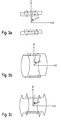
- FIG. 1 shows a deflection arrangement 1 according to the invention comprises a magnetic lens doublet 3 with two magnetic lenses 5 and 7, which are for electrons of 100 keV energy, respectively have a focal length f of 180 mm.
- the magnetic lens doublet 3 is used to map one in an object plane 9 of the doublet 3 arranged beam shaping aperture 11 on one arranged in an image plane 13 of the doublet 3 Mask 15. Defines the beam shaping diaphragm 11 the mask 15 a sharply outlined illuminated field 16.
- Each the magnetic lenses 5 and 7 comprise a winding 18 and pole pieces 17 in order to create a focusing magnetic field with the Provide focal length f.
- the bore diameter of the Pole is 80 mm and the pole shoe gap is 40 mm.
- the magnetic lenses 5 and 7 are each symmetrical about one Axis of symmetry 19 of the doublet 3 and at a distance of 2 f arranged from each other.
- the beam shaping aperture 11 is included their center also arranged on the axis of symmetry 19.
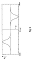
- the course of the axial component B z in the direction of the axis of symmetry 19 of the magnetic field generated by the lenses 5 and 7 is shown in FIG. 5 in arbitrary units.
- the course of the field is such that a crossover point 23 is formed in a plane of symmetry 21 of the doublet 3 for an electron beam passing through the doublet (antisymmetric doublet).
- the lens 5 centrally penetrating electron beam by an amount M laterally the axis of symmetry 19 offset.
- the one through the deflection unit 25 particle beam offset by the amount M from the axis of symmetry 19 27 thus occurs decentrally in the lens 7 of the doublet 3, its offset by the amount M of the Axis of symmetry 19 is maintained, so that it also around the amount M strikes the mask 15. nevertheless however, the beam 27 passes through the lens 7 onto the image plane 13 focused.
- the necessary for this purpose Magnetic field is provided by the focusing Field of the lens 7, which by the coil 15 and the Pole shoes 17 is provided, a correction magnetic field is superimposed by an axle shifting device 29 is generated.
- the axle displacement device 29 comprises two deflection windings 31 and 33, each radial within radially inward to the axis of symmetry 19 indicative ends 35 of the pole piece 17 of the lens 7 arranged are.
- the deflection windings 31 and 33 here are transverse magnetic field directed towards the axis of symmetry 19, whose size is proportional to the first derivative of that in FIG. 5 shown axial component of the generated by the lens 7 Magnetic field.
- Such a course of the correction magnetic field is by suitable choice of the geometry for the deflection coils 31 and 33 possible.
- the correction magnetic field is also proportional to the size the axis offset generated by the beam displacement arrangement M and points in its direction.
- Each of the lenses 5 and 7 further comprises a stigmator winding 37 to correct an astigmatic aberration the lens 5 or 7 and a dynamic focus coil 39 by a focus error of the field curvature of the lens 5 or 7 to correct.
- the radiation displacement assembly 25 includes two the symmetry plane 21 symmetrical deflection coils 41 and 43 and another arranged on the axis of symmetry 21 dynamic focus coil 45.
- FIG. 3 Possible embodiments for turns of the deflection coils 31, 33, 41 and 43 are shown schematically in FIG. 3. in this connection 3a shows the execution of turns as a toroid coil, Figure 3b the execution as a saddle coil and Figure 3c the design as a composite saddle coil.
- a stack 49 of nine Ferrite rings 51 of the same diameter are arranged equidistantly.
- the ferrite rings 55 of the inner set 53 have an inner radius Ri of 28 mm and an outer radius Ra of 32 mm.
- the deflection windings 31 and 33 encompass each of them axially outer three ferrite rings 55 of the inner stack 53, while the stigmator winding 37 the middle in the axial direction Grips ferrite ring 55 of stack 53.
- the dynamic Focus coil 39 is made radially inside the inner stack 53 Ferrite rings 55 arranged. Axial centers of the coils 31, 33 each point from a plane of symmetry 56 of the lens 7 an axial distance s of 23 mm; the axial length of the Coils 31 and 33 are also 24 mm each.
- the distribution of the turns of the deflection windings 31 and 33 4 can be seen in the circumferential direction of the ferrite rings 55.
- FIG. 4a shows the turns which are used to generate a magnetic dipole field By directed in a y direction
- FIG. 4b shows turns which are used to generate a dipole field B x orthogonal to this
- FIG. 4c shows the combination of the turns shown in FIGS. 4a and 4b on the ferrite rings 55.
- the arrangement of the windings 41 and 43 of the radiation displacement arrangement 25 can be seen in detail from FIG.
- the Radiation displacement assembly 25 includes a set 59 of 17 Ferrite rings 61 of the same diameter, which are equidistant in Arranged axially and symmetrically to the axis of symmetry 21 are. Radially outside of each ferrite ring 61 is one Ferrite ring 63 of larger diameter of a second set 65 arranged by ferrite rings.
- the deflection coils 41 and 43 are wound on ferrite rings 61 of the radially inner set 59, the turn shown in Figures 3a to 3c Forms of turns are possible.
- the distribution in the circumferential direction corresponds to the ferrite rings 61 of the turns again the arrangement shown in Figure 4.
- the Windings of the deflection windings 41 and 43 encompass the seen from the axially outside, second to sixth ferrite rings 61.
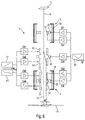
- FIG 6 is a functional diagram for controlling the individual windings of the deflection arrangement shown in Figure 1 1 explained.
- the windings 18 of the lenses 5 and 7 of the doublet 3 are driven with a constant current, so that each of the lenses 5 and 7 has a focal length f of Provides 180 mm for the electrons.
- the proportionality constants are included Cd1 and Cd2 designated.
- the Coils 31 and 33 of the lens 7 also with a current driven, which has a proportional portion 61, wherein the corresponding proportionality constants with Cd3 and Cd4 are designated.
- a current driven which has a proportional portion 61, wherein the corresponding proportionality constants with Cd3 and Cd4 are designated.
- the ratios of the proportionality constants Cd1, Cd2, Cd3 and Cd4, with ideal adherence to the geometry in the manufacture of the arrangement, preferably satisfy the relation
- 1.
- Radiation displacement arrangement 25 and axis displacement device 29 it is possible to use the beam shaping diaphragm 11 very slight distortions on an illuminated field 16 the mask 15, with the illuminated field 16 off the axis of symmetry 19 can be moved out. A steepness (Increase in intensity from 20% to 80%) to the Edges of the illuminated field 16 of 0.2 ⁇ m can be achieved become.
- the imaging beam 25, 27 passes through both the field shaping aperture 11 and the mask 15 are vertical (Telecentricity).
- the ring sets 49, 53, 59 and 65 can, for example, as follows are manufactured:
- FIGS. 1 to 8 Variants of those shown in FIGS. 1 to 8 are described below shown deflection arrangement explained. Regarding her Structure and their corresponding components are designated by the reference numbers from FIGS. 1 to 8, for distinction, however, with an additional letter Mistake. For explanation, reference is made to the entire preceding Description referred.
- Figure 9 shows a magnetic lens doublet 3b of focusing Magnetic lenses 5b and 7b.
- the doublet 3b serves one in mask 15b arranged on an object plane 9b of doublet 3b on one arranged in an image plane 13b of the doublet Imaging semiconductor wafer 75.
- a Electron beam directed onto the mask 15b for which purpose, for example the arrangement shown in Figure 1 can be used can, which by means of a beam shaping aperture a well Defined field illuminated on the mask 15b.
- the electron beam is deflected with respect to an axis of symmetry 19b, uniformly and in stripes around the illuminated field to move over the mask 15b.
- Figure 9 is the beam path a central ray of the illuminated field for three different deflection positions M are shown.
- the doublet 3b offers a 1: 4 reduction Image of the mask 15b on the wafer 75 two lenses 5b and 7b "symmetrically" with respect to a plane of symmetry 21b of the doublet 3b.
- the symmetry is here not to be understood in the strictly geometric sense, but taking into account the reduction 1: 4, whereby also the Size relationships of the two lenses 5b and 7b and their Scale distances to the plane of symmetry 21b as 1: 4.
- FIG. 10 shows an electron microscopy system 81, which works as a scanning electron microscope.
- This includes a sample holder 83 for receiving a sample 85 with a Sample surface 87 such that an area to be observed the sample surface 87 with respect to a major axis 19c of the Microscope 81 is centered.
- An electron source 89 emits a divergent bounded by an aperture diaphragm 91
- Electron beam 90 from a lens 93 such that is focused in the plane of a scattering electron aperture 95 a reduced image of the electron source 89 is produced.
- the reduced image of the electron source will by means of a magnetic lens doublet 3c on the sample surface 87 mapped, so there in the area of a point 97 the smallest possible spot of the sample surface 87 is illuminated becomes.
- the on the sample surface 87 with a Energy of, for example, 20 keV occurring electrons
- Electron source 89 generate secondary electrons there, which by means of an auxiliary field to an electron detector 99 be drawn in and registered by the latter.
- the magnetic lens doublet 3c has a structure that in essentially the structure of the magnetic lens doublet shown in Figure 1 corresponds, and here it is also a Deflection arrangement 25c provided to the of the electrons illuminated point 97 on the sample surface 87 by one deflect changeable amount M from the axis of symmetry 19c.
- the lens 7c also has one in FIG. 10 Axis shift device, not shown, so that even with comparatively large deflection values M of the illuminated Point 97 from the main axis 19c a precise and fine focused image of the reduced image of source 89 in level 95 and thus a high resolution of the electron microscope 89 can be achieved.
- the lens doublet 3c can be a symmetrical doublet, the lenses 5c and 7c have the same focal lengths. This has the advantage that certain aberrations of the Compensate lenses 5c or 7c and a particularly finely focused one Image of the source essentially independent of the Deflection M can be generated on the sample surface 87.
- the Use of the symmetrical magnetic lens doublet 3c Focusing in particular enables imaging with a particularly low coma error.
- the doublet 3c but also be constructed asymmetrically, the Focal lengths of the lenses 5c and 7c are different. Also here certain aberrations of the lenses are compensated partially. In particular, the lens 7c then has a smaller one Focal length than the lens 5c, so that further reduction of the image generated in the plane of the aperture 95 Electron source 89 is generated on the sample surface 87.
- Figure 11 shows a variant of that shown in Figure 10 Electron microscope.
- the electron microscope 81 of FIG. 11 differs from the microscope shown in FIG only one focusing lens 7d to one of one Electron source 89d emitted and through an aperture stop 91d shaped divergent beam 90d onto a sample surface Focus 87d.
- the focusing lens 7d is like that beam 90d initially emitted by electron source 89d, centered with respect to an axis of symmetry 19d.
- a deflection unit 25d provided to the beam 90d by an amount M to be offset parallel to the axis of symmetry 19d.
- the deflector For this purpose, 25d comprises deflection coils 41d and 43d and a dynamic focus coil 45d.
- the electron beam then enters the focusing lens 7d, which has an axle displacement device 29d, around also the center of that provided by the lens 7d Deflection field in accordance with the offset Electron beam by the amount M from the axis of symmetry 19d wegzuver## So that the lens 7d for the beam Effect of a centrally penetrating focusing lens, and a Point 97d where the beam focuses on the sample surface 87d is also related to the amount M the axis of symmetry 19d deflected.
- FIG. 12 shows an electron microscopy system 81e, which works as a transmission electron microscope.
- a sample 85e is taken from one side illuminated with electrons in an extended field 16e, and those passing through the sample 85e in the field 16e Transmission electrons are created using imaging optics 101 is imaged on a spatially resolving detector 99e.
- the Object 85e here is a lithography mask to represent one Structure 102 on a wafer in a lithography process.
- the Quality of structure 102 is assessed using the electron microscope 81e checked.
- the imaging optics 101 is included formed such that the entire illuminated field 16e the detector 99e is imaged.
- the imaging optics 101 in such a way that the field 16e, which is imaged on the detector 99e from an axis of symmetry 19e of the microscope 81e out by an adjustable Amount M is shiftable.
- the imaging optics 101 after changing the Deflection M different areas of the Sample 85e are imaged on the detector 99e so that overall a comparatively large area of sample 85e can be examined without this relative to the microscope 81e to move mechanically.
- an illumination system 103 for illuminating the The area 16e imaged in the detector 99e is designed in such a way that that not the entire sample surface 85e at the same time is illuminated with electrons, only the Area 16e that is on detector 99e at a time is mapped.
- the illumination optics 103 comprise a focusing lens doublet 3e with focusing lenses 5e and 7e, which sequentially from one emitted from an electron source 89e and an aperture stop 91e shaped electron beam 90d are run through. Between the two lenses 5e and 7e is a deflection unit 25e with deflection coils 41e and 43e provided to extend the beam 90d by an amount M from the To shift axis of symmetry 19e.
- the one from the axis of symmetry 19e displaced beam 90d then enters the second Focussing lens 7e and is so by this on the Sample surface 85e directed that there is only the area 16e is illuminated, which is also by the amount M of the axis of symmetry 19e is shifted away.
- 7e includes an axle displacement device 29e two deflection windings 31e and 33e, also a dynamic one Focus coil 45e is provided.
- the imaging system 101 for imaging the area 16e emerging transmission electrons on the detector 99e comprises a lens doublet 3e 'and for further enlargement a magnetic lens 105.
- the lens doublet 3e ' is made up of components that are related to sample 85e symmetrical to the components of the lens doublet 3e Illumination optics 103 are arranged.
- a deflection unit 25e' provided whose components are also related to the sample 85e symmetrical to the components of the deflection unit 25e are arranged.
- the components of the lens doublet 3e 'and the deflection unit 25e 'of the imaging optics 101 are in view to this symmetry with the same reference numerals as the corresponding components of the illumination optics 103 designated, but additionally provided with an apostrophe.
- the imaging optics 101 form an object size 107 above Intermediate image 109 into an image 110 on the detector 99e.
- a control is shown in FIG. 12 with reference number 112 denotes which currents in the coils 41e, 43e, 31e, 33e, 45e and 33e ', 31e', 45e ', 43e' and 41e ' that both the lighting of field 16e and its Imaging onto the detector 99e when the field is deflected 16e by the amount M away from the axis of symmetry 19e high quality.
Landscapes
- Chemical & Material Sciences (AREA)
- Analytical Chemistry (AREA)
- Electron Beam Exposure (AREA)
- Electron Sources, Ion Sources (AREA)
Applications Claiming Priority (2)
| Application Number | Priority Date | Filing Date | Title |
|---|---|---|---|
| DE10044199A DE10044199B9 (de) | 2000-09-07 | 2000-09-07 | Ablenkanordnung und Projektionssystem für geladene Teilchen |
| DE10044199 | 2000-09-07 |
Publications (2)
| Publication Number | Publication Date |
|---|---|
| EP1187169A2 true EP1187169A2 (fr) | 2002-03-13 |
| EP1187169A3 EP1187169A3 (fr) | 2007-11-07 |
Family
ID=7655369
Family Applications (1)
| Application Number | Title | Priority Date | Filing Date |
|---|---|---|---|
| EP01121374A Withdrawn EP1187169A3 (fr) | 2000-09-07 | 2001-09-06 | Composants d'optique corpusculaire et dispositif comportant de tels composants |
Country Status (6)
| Country | Link |
|---|---|
| US (1) | US6642525B2 (fr) |
| EP (1) | EP1187169A3 (fr) |
| JP (1) | JP2002164011A (fr) |
| KR (1) | KR100898971B1 (fr) |
| DE (1) | DE10044199B9 (fr) |
| TW (1) | TW541567B (fr) |
Cited By (1)
| Publication number | Priority date | Publication date | Assignee | Title |
|---|---|---|---|---|
| WO2011069493A1 (fr) * | 2009-12-10 | 2011-06-16 | Ferrotec Gmbh | Dispositif de déviation pour faisceaux d'électrons, unité de déviation magnétique pour un tel dispositif de déviation et dispositif pour vaporiser un substrat plat muni d'un tel dispositif de déviation |
Families Citing this family (21)
| Publication number | Priority date | Publication date | Assignee | Title |
|---|---|---|---|---|
| DE10044199B9 (de) | 2000-09-07 | 2005-07-28 | Carl Zeiss Smt Ag | Ablenkanordnung und Projektionssystem für geladene Teilchen |
| TW579536B (en) | 2001-07-02 | 2004-03-11 | Zeiss Carl Semiconductor Mfg | Examining system for the particle-optical imaging of an object, deflector for charged particles as well as method for the operation of the same |
| DE10136190A1 (de) * | 2001-07-25 | 2003-02-06 | Ceos Gmbh | Schlitzlinsenanordnung für Teilchenstrahlen |
| DE10159308A1 (de) * | 2001-12-04 | 2003-06-12 | Ceos Gmbh | Teilchenoptischer Korrektor |
| DE10230929A1 (de) | 2002-07-09 | 2004-01-29 | Leo Elektronenmikroskopie Gmbh | Verfahren zum elektronenmikroskopischen Beobachten einer Halbleiteranordnung und Vorrichtung hierfür |
| DE10232689A1 (de) * | 2002-07-18 | 2004-02-05 | Leo Elektronenmikroskopie Gmbh | Mit Strahlen geladener Teilchen arbeitende Anwendungen |
| DE10235455B9 (de) | 2002-08-02 | 2008-01-24 | Leo Elektronenmikroskopie Gmbh | Teilchenoptische Vorrichtung und Verfahren zum Betrieb derselben |
| US7157703B2 (en) | 2002-08-30 | 2007-01-02 | Ebara Corporation | Electron beam system |
| JP3968334B2 (ja) * | 2002-09-11 | 2007-08-29 | 株式会社日立ハイテクノロジーズ | 荷電粒子線装置及び荷電粒子線照射方法 |
| US20080026077A1 (en) * | 2002-11-12 | 2008-01-31 | John Hilfinger | Methods and compositions of gene delivery agents for systemic and local therapy |
| JP2007525249A (ja) * | 2003-06-02 | 2007-09-06 | フォックス・チェイス・キャンサー・センター | 高エネルギー連続エネルギーイオン選択システム、イオン線治療システム、およびイオン線治療施設 |
| CN101014383A (zh) * | 2003-12-02 | 2007-08-08 | 福克斯·彻斯癌症中心 | 调制用于放射治疗的激光-加速质子的方法 |
| DE102004019835B4 (de) * | 2004-04-23 | 2007-08-02 | Vistec Electron Beam Gmbh | Beleuchtungskondensor für ein Partikeloptik-Projektionssystem |
| DE102004019834B4 (de) * | 2004-04-23 | 2007-03-22 | Vistec Electron Beam Gmbh | Korrekturlinsen-System für ein Partikelstrahl-Projektionsgerät |
| EP1914785B1 (fr) * | 2006-10-20 | 2016-09-14 | JEOL Ltd. | Correcteur d'aberrations et procédé pour la correction d'aberrations |
| JP5097512B2 (ja) * | 2006-11-21 | 2012-12-12 | 株式会社日立ハイテクノロジーズ | 荷電粒子ビーム用軌道補正器、及び荷電粒子ビーム装置 |
| US8878147B2 (en) * | 2010-09-07 | 2014-11-04 | Joseph C. Robinson | Method and apparatus for in situ preparation of serial planar surfaces for microscopy |
| JP5879549B2 (ja) * | 2011-09-20 | 2016-03-08 | パナソニックIpマネジメント株式会社 | ライトフィールド撮像装置、および画像処理装置 |
| US20190287759A1 (en) * | 2014-01-27 | 2019-09-19 | Mochii, Inc. (D/B/A Voxa) | Transmission Electron Microscopy |
| TWI506666B (zh) | 2014-08-08 | 2015-11-01 | Nat Univ Tsing Hua | 桌上型電子顯微鏡及其複合多極-聚焦可調式磁透鏡 |
| US9799484B2 (en) | 2014-12-09 | 2017-10-24 | Hermes Microvision, Inc. | Charged particle source |
Citations (6)
| Publication number | Priority date | Publication date | Assignee | Title |
|---|---|---|---|---|
| US4376249A (en) * | 1980-11-06 | 1983-03-08 | International Business Machines Corporation | Variable axis electron beam projection system |
| US5530251A (en) * | 1994-12-21 | 1996-06-25 | International Business Machines Corporation | Inductively coupled dual-stage magnetic deflection yoke |
| US5747819A (en) * | 1995-11-01 | 1998-05-05 | Nikon Corporation | Charged particle beam transfer device exhibiting low aberration |
| US5757010A (en) * | 1996-12-18 | 1998-05-26 | International Business Machines Corporation | Curvilinear variable axis lens correction with centered dipoles |
| US5793048A (en) * | 1996-12-18 | 1998-08-11 | International Business Machines Corporation | Curvilinear variable axis lens correction with shifted dipoles |
| US6060711A (en) * | 1997-01-27 | 2000-05-09 | Nikon Corporation | Charged-particle optical systems and pattern transfer apparatus comprising same |
Family Cites Families (37)
| Publication number | Priority date | Publication date | Assignee | Title |
|---|---|---|---|---|
| US3984687A (en) * | 1975-03-17 | 1976-10-05 | International Business Machines Corporation | Shielded magnetic lens and deflection yoke structure for electron beam column |
| JPS57206173A (en) | 1981-06-15 | 1982-12-17 | Nippon Telegr & Teleph Corp <Ntt> | Focusing deflecting device for charged corpuscule beam |
| US4544846A (en) | 1983-06-28 | 1985-10-01 | International Business Machines Corporation | Variable axis immersion lens electron beam projection system |
| NL8602177A (nl) | 1986-08-27 | 1988-03-16 | Philips Nv | Electronen detectie met energie discriminatie. |
| KR920000941B1 (ko) * | 1988-02-16 | 1992-01-31 | 후지쓰 가부시끼가이샤 | 전자빔 노광장치 |
| NL8801208A (nl) | 1988-05-09 | 1989-12-01 | Philips Nv | Geladen deeltjes bundel apparaat. |
| US4945246A (en) | 1989-03-24 | 1990-07-31 | International Business Machines Corporation | Tri-deflection electron beam system |
| US5258246A (en) | 1989-08-07 | 1993-11-02 | At&T Bell Laboratories | Device manufacture involving lithographic processing |
| US5264706A (en) * | 1991-04-26 | 1993-11-23 | Fujitsu Limited | Electron beam exposure system having an electromagnetic deflector configured for efficient cooling |
| US5285074A (en) | 1992-06-03 | 1994-02-08 | International Business Machines Corporation | Dynamic compensation of non-linear electron beam landing angle in variable axis lenses |
| US5389858A (en) | 1992-07-16 | 1995-02-14 | International Business Machines Corporation | Variable axis stigmator |
| US5382498A (en) | 1992-12-16 | 1995-01-17 | At&T Corp. | Processes for electron lithography |
| US5674413A (en) | 1993-12-23 | 1997-10-07 | International Business Machines Corporation | Scattering reticle for electron beam systems |
| US5466904A (en) * | 1993-12-23 | 1995-11-14 | International Business Machines Corporation | Electron beam lithography system |
| US5523580A (en) | 1993-12-23 | 1996-06-04 | International Business Machines Corporation | Reticle having a number of subfields |
| US5545920A (en) * | 1994-09-13 | 1996-08-13 | Texas Instruments Incorporated | Leadframe-over-chip having off-chip conducting leads for increased bond pad connectivity |
| US5633507A (en) | 1995-09-19 | 1997-05-27 | International Business Machines Corporation | Electron beam lithography system with low brightness |
| US5770863A (en) | 1995-10-24 | 1998-06-23 | Nikon Corporation | Charged particle beam projection apparatus |
| JP3455006B2 (ja) | 1996-03-25 | 2003-10-06 | 株式会社東芝 | 荷電粒子ビーム装置 |
| US5635719A (en) | 1996-07-23 | 1997-06-03 | International Business Machines Corporation | Variable curvilinear axis deflection means for particle optical lenses |
| JPH1040848A (ja) | 1996-07-25 | 1998-02-13 | Nikon Corp | 荷電粒子線装置 |
| JPH1097979A (ja) | 1996-09-25 | 1998-04-14 | Nikon Corp | 縮小投影装置 |
| US5825043A (en) | 1996-10-07 | 1998-10-20 | Nikon Precision Inc. | Focusing and tilting adjustment system for lithography aligner, manufacturing apparatus or inspection apparatus |
| US5747814A (en) | 1996-12-06 | 1998-05-05 | International Business Machines Corporation | Method for centering a lens in a charged-particle system |
| US5708274A (en) | 1996-12-18 | 1998-01-13 | International Business Machines Corporation | Curvilinear variable axis lens correction with crossed coils |
| US6064071A (en) * | 1997-04-23 | 2000-05-16 | Nikon Corporation | Charged-particle-beam optical systems |
| JPH10303117A (ja) | 1997-04-30 | 1998-11-13 | Nikon Corp | 電子線光学系 |
| JPH10303118A (ja) | 1997-04-30 | 1998-11-13 | Nikon Corp | 電子線投影光学系 |
| JPH1131470A (ja) | 1997-07-08 | 1999-02-02 | Nikon Corp | 電子光学系 |
| JPH1173900A (ja) | 1997-08-28 | 1999-03-16 | Nikon Corp | 荷電粒子線光学系 |
| US6066855A (en) | 1997-10-07 | 2000-05-23 | Nikon Corporation | Charged-particle-beam optical system exhibiting aberration correction |
| US6069684A (en) | 1998-02-04 | 2000-05-30 | International Business Machines Corporation | Electron beam projection lithography system (EBPS) |
| EP0969326B1 (fr) * | 1998-07-01 | 2012-10-17 | ASML Netherlands B.V. | Appareil lithographique |
| US6023067A (en) | 1998-08-22 | 2000-02-08 | Nikon Corporation | Blanking system for electron beam projection system |
| US6005250A (en) | 1998-08-22 | 1999-12-21 | Nikon Corporation | Illumination deflection system for E-beam projection |
| US6420713B1 (en) * | 1999-04-28 | 2002-07-16 | Nikon Corporation | Image position and lens field control in electron beam systems |
| DE10044199B9 (de) | 2000-09-07 | 2005-07-28 | Carl Zeiss Smt Ag | Ablenkanordnung und Projektionssystem für geladene Teilchen |
-
2000
- 2000-09-07 DE DE10044199A patent/DE10044199B9/de not_active Expired - Fee Related
-
2001
- 2001-09-06 TW TW090122060A patent/TW541567B/zh not_active IP Right Cessation
- 2001-09-06 KR KR1020010054790A patent/KR100898971B1/ko not_active IP Right Cessation
- 2001-09-06 EP EP01121374A patent/EP1187169A3/fr not_active Withdrawn
- 2001-09-07 JP JP2001272363A patent/JP2002164011A/ja not_active Withdrawn
- 2001-09-07 US US09/949,193 patent/US6642525B2/en not_active Expired - Fee Related
Patent Citations (6)
| Publication number | Priority date | Publication date | Assignee | Title |
|---|---|---|---|---|
| US4376249A (en) * | 1980-11-06 | 1983-03-08 | International Business Machines Corporation | Variable axis electron beam projection system |
| US5530251A (en) * | 1994-12-21 | 1996-06-25 | International Business Machines Corporation | Inductively coupled dual-stage magnetic deflection yoke |
| US5747819A (en) * | 1995-11-01 | 1998-05-05 | Nikon Corporation | Charged particle beam transfer device exhibiting low aberration |
| US5757010A (en) * | 1996-12-18 | 1998-05-26 | International Business Machines Corporation | Curvilinear variable axis lens correction with centered dipoles |
| US5793048A (en) * | 1996-12-18 | 1998-08-11 | International Business Machines Corporation | Curvilinear variable axis lens correction with shifted dipoles |
| US6060711A (en) * | 1997-01-27 | 2000-05-09 | Nikon Corporation | Charged-particle optical systems and pattern transfer apparatus comprising same |
Non-Patent Citations (1)
| Title |
|---|
| PFEIFFER H C ET AL: "ADVANCED DEFLECTION CONCEPT FOR LARGE AREA, HIGH RESOLUTION E-BEAM LITHOGRAPHY" JOURNAL OF VACUUM SCIENCE AND TECHNOLOGY, NEW YORK, NY, US, Bd. 19, Nr. 4, November 1981 (1981-11), Seiten 1058-1063, XP009054054 ISSN: 0022-5355 * |
Cited By (2)
| Publication number | Priority date | Publication date | Assignee | Title |
|---|---|---|---|---|
| WO2011069493A1 (fr) * | 2009-12-10 | 2011-06-16 | Ferrotec Gmbh | Dispositif de déviation pour faisceaux d'électrons, unité de déviation magnétique pour un tel dispositif de déviation et dispositif pour vaporiser un substrat plat muni d'un tel dispositif de déviation |
| US9218936B2 (en) | 2009-12-10 | 2015-12-22 | Ferrotec Europe Gmbh | Deflecting device for electron beams, magnetic deflecting unit for such a deflecting device, and device for vapor coating a planar substrate using such a deflecting device |
Also Published As
| Publication number | Publication date |
|---|---|
| TW541567B (en) | 2003-07-11 |
| EP1187169A3 (fr) | 2007-11-07 |
| JP2002164011A (ja) | 2002-06-07 |
| KR20020020231A (ko) | 2002-03-14 |
| DE10044199A1 (de) | 2002-06-06 |
| DE10044199B4 (de) | 2005-03-03 |
| US6642525B2 (en) | 2003-11-04 |
| KR100898971B1 (ko) | 2009-05-25 |
| DE10044199B9 (de) | 2005-07-28 |
| US20020084422A1 (en) | 2002-07-04 |
Similar Documents
| Publication | Publication Date | Title |
|---|---|---|
| EP1187169A2 (fr) | Composants d'optique corpusculaire et dispositif comportant de tels composants | |
| DE102018007652B4 (de) | Teilchenstrahl-System sowie Verfahren zur Stromregulierung von Einzel-Teilchenstrahlen | |
| EP1280184B9 (fr) | Système d'inspection d'optique corpusculaire pour l'imagerie d'un objet, dispositif pour la déflection des particules chargées et procédé pour son fonctionnement | |
| EP0333018B1 (fr) | Lentille d'objectif pour la focalisation de particules chargées | |
| EP1385193B9 (fr) | Lentille d'objectif pour système de microscopie électronique, et système de microscopie électronique | |
| DE2842527B2 (de) | Elektrostatische Emissionslinse | |
| EP0274622A1 (fr) | Assemblage de détecteur avec un objectif muni d'un détecteur pour instruments à rayons corpusculaires | |
| DE112015001235B4 (de) | Vorrichtung und verfahren zur abbildung mittels eines elektronenstrahls unter verwendung eines monochromators mit doppeltem wien-filter sowie monochromator | |
| EP3712924B1 (fr) | Dispositif et procédé de transfert d'électrons d'un échantillon à un analyseur d'énergie et dispositif spectromètre d'électrons | |
| DE69920182T2 (de) | Korpuskularstrahloptisches gerät mit auger-elektronendetektion | |
| DE102018115012A1 (de) | Teilchenstrahlsystem | |
| EP0911860B1 (fr) | Appareil à faisceau de particules chargées avec filtre en énergie | |
| DE69202782T2 (de) | Feldemissions-Elektronenkanone geringer Aberration. | |
| EP1239510B1 (fr) | Assemblage de lentilles optiques à particules et méthode utilisante un tel assemblage de lentilles | |
| EP1738392B1 (fr) | Condensateur d'eclairage destine a un systeme projecteur a particules | |
| DE102010001346A1 (de) | Teilchenstrahlgerät und Verfahren zum Betreiben eines Teilchenstrahlgeräts | |
| EP0564438A1 (fr) | Système de formation d'images par faisceau de particules notamment système d'imagerie en optique ionique | |
| EP1410416B1 (fr) | Systeme de lentilles a fentes pour faisceaux de particules | |
| DE102020102854B4 (de) | Teilchenstrahlgerät | |
| DE10190535B4 (de) | Emissionselektronenmikroskop | |
| DE10131931A1 (de) | Untersuchungssystem zum teilchenoptischen Abbilden eines Objekts, Ablenkvorrichtung für geladene Teilchen sowie Verfahren zum Betrieb derselben | |
| DE102014019408A1 (de) | Abbildende Energiefiltervorrichtung und Verfahren zu deren Betrieb | |
| WO2003052790A2 (fr) | Systeme de lentilles presentant un axe optique lateralement deplaçable conçu pour un rayonnement corpusculaire | |
| DE69913100T2 (de) | Projektionslithographie mittels ladungsträgern | |
| DE3017365C2 (de) | Korpuskularstrahlgerät zur Erzeugung eines Bestrahlungsmusters auf einem Werkstück und Verfahren zum Betrieb |
Legal Events
| Date | Code | Title | Description |
|---|---|---|---|
| PUAI | Public reference made under article 153(3) epc to a published international application that has entered the european phase |
Free format text: ORIGINAL CODE: 0009012 |
|
| AK | Designated contracting states |
Kind code of ref document: A2 Designated state(s): AT BE CH CY DE DK ES FI FR GB GR IE IT LI LU MC NL PT SE TR |
|
| AX | Request for extension of the european patent |
Free format text: AL;LT;LV;MK;RO;SI |
|
| RAP1 | Party data changed (applicant data changed or rights of an application transferred) |
Owner name: CARL ZEISS SMT AG |
|
| RAP1 | Party data changed (applicant data changed or rights of an application transferred) |
Owner name: CARL ZEISS SMT AG |
|
| PUAL | Search report despatched |
Free format text: ORIGINAL CODE: 0009013 |
|
| AK | Designated contracting states |
Kind code of ref document: A3 Designated state(s): AT BE CH CY DE DK ES FI FR GB GR IE IT LI LU MC NL PT SE TR |
|
| AX | Request for extension of the european patent |
Extension state: AL LT LV MK RO SI |
|
| 17P | Request for examination filed |
Effective date: 20080505 |
|
| 17Q | First examination report despatched |
Effective date: 20080611 |
|
| AKX | Designation fees paid |
Designated state(s): DE FR GB NL |
|
| GRAP | Despatch of communication of intention to grant a patent |
Free format text: ORIGINAL CODE: EPIDOSNIGR1 |
|
| STAA | Information on the status of an ep patent application or granted ep patent |
Free format text: STATUS: THE APPLICATION IS DEEMED TO BE WITHDRAWN |
|
| 18D | Application deemed to be withdrawn |
Effective date: 20100622 |