EP1184986B1 - LVDS circuits connected in series for the supply current - Google Patents
LVDS circuits connected in series for the supply current Download PDFInfo
- Publication number
- EP1184986B1 EP1184986B1 EP20010307196 EP01307196A EP1184986B1 EP 1184986 B1 EP1184986 B1 EP 1184986B1 EP 20010307196 EP20010307196 EP 20010307196 EP 01307196 A EP01307196 A EP 01307196A EP 1184986 B1 EP1184986 B1 EP 1184986B1
- Authority
- EP
- European Patent Office
- Prior art keywords
- circuit
- current
- current steering
- line driver
- steering stage
- Prior art date
- Legal status (The legal status is an assumption and is not a legal conclusion. Google has not performed a legal analysis and makes no representation as to the accuracy of the status listed.)
- Expired - Lifetime
Links
- 238000000034 method Methods 0.000 claims description 14
- 230000000087 stabilizing effect Effects 0.000 claims 3
- 238000003491 array Methods 0.000 description 20
- 238000004064 recycling Methods 0.000 description 15
- 230000005540 biological transmission Effects 0.000 description 12
- 238000010586 diagram Methods 0.000 description 11
- 101100102627 Oscarella pearsei VIN1 gene Proteins 0.000 description 5
- 238000005192 partition Methods 0.000 description 2
- 239000004065 semiconductor Substances 0.000 description 2
- 239000002131 composite material Substances 0.000 description 1
- 230000007423 decrease Effects 0.000 description 1
- 230000002939 deleterious effect Effects 0.000 description 1
- 230000001419 dependent effect Effects 0.000 description 1
- 239000000284 extract Substances 0.000 description 1
- 238000000605 extraction Methods 0.000 description 1
- 230000036039 immunity Effects 0.000 description 1
- 230000003116 impacting effect Effects 0.000 description 1
- 229910044991 metal oxide Inorganic materials 0.000 description 1
- 150000004706 metal oxides Chemical class 0.000 description 1
- 230000001902 propagating effect Effects 0.000 description 1
Images


Classifications
-
- H—ELECTRICITY
- H03—ELECTRONIC CIRCUITRY
- H03K—PULSE TECHNIQUE
- H03K19/00—Logic circuits, i.e. having at least two inputs acting on one output; Inverting circuits
- H03K19/0008—Arrangements for reducing power consumption
- H03K19/0019—Arrangements for reducing power consumption by energy recovery or adiabatic operation
Definitions
- the present invention relates to the field of circuits and, more particularly, to a method and apparatus for current recycling for circuits.
- FIG. 10 An example of a conventional low voltage differential swing (LVDS) driver circuit 800 used for differential data transmission is shown in Figure 10.
- a pair of differential signals means two signals whose current waveforms are out of phase with one another.
- the individual signals of a pair of differential signals are indicated by reference symbols respectively ending with "+” and "-" notation (e.g., S+ and S-).
- the composite notation "+/-" is employed to indicate both differential signals using a single reference symbol, e.g., S+/-.
- the LVDS driver circuit 800 includes a direct current (DC) constant current source I1 coupled to voltage supply VDD, four n-channel metal oxide semiconductor (NMOS) switches M11-M14, and a resistor R1 coupled between the common node COM and voltage supply VSS.
- the four transistor switches M11-M14 are controlled by input voltage signals VIN1, VIN2 and direct current through load resistor Rt as indicated by arrows A and B.
- the input voltage signals VIN1, VIN2 are typically rail-to-rail voltage swings.
- the gates of NMOS switches M11 and M14 couple together to receive input voltage signal VIN1.
- the gates of NMOS switches M12 and M13 couple together to receive input voltage signal VIN2.
- the prior differential LVDS driver circuit 800 sources current from VDD and sinks this current to VSS.
- a switching array controlled by a Boolean signal routes the source current through the interconnect to an external resistive load.
- the return current is routed back to the array and sunk to VSS.
- the polarity of the voltage drop across the resistor carries the digital value. Changing the polarity of the array causes the current to route through the interconnect and resistor in the opposite direction and transfer the other digital value.
- the differential LVDS offers reduced power consumption as compared with other drivers.
- the disadvantage is the need to have a set of interconnects for each signal because a differential LVDS driver is provided for each of the interconnects. It is this need to have a set of interconnects for each signal that drives the power of an integrated circuit using differential LVDS driver circuits.
- the present invention is directed to a process and circuitry for drawing current from a power source to produce a first operation, such as a Boolean operation, and reusing the current to generate a further operation.
- a first operation such as a Boolean operation
- the current from the first operation may be used to perform a second or subsequent operation instead of sinking the current to ground or another power source. This process is referred generally herein as current recycling.
- the present invention provides a process for drawing current from a power source to produce a first operation, such as a Boolean operation, and reusing the current to generate further operations.
- a first operation such as a Boolean operation
- the current from the first operation may be used to perform a second or subsequent operation.
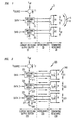
- FIG. 1 is a block diagram of a line driver 5 useful for illustrating an exemplary embodiment of the present invention.
- the line driver 5 includes current recycling output buffer 10 that has at least a first switching array 15 and a second switching array 20.
- the current recycling buffer 10 is electrically coupled to an interconnect section 25 which is in turn electrically coupled to a load that forms a terminating resistance 30.
- the switching arrays 15, 20 are arranged so that the current I1 being supplied from the supply Vdd is applied to the first switching array 15.
- the first switching array 15 routes the current to the terminating resistance and back transferring a first Boolean operation, shown as V s1 , across the load R1.
- the current I2 is applied to the second switching array 20 so that the second switching array 20 can perform a second Boolean operation, shown as V s2 , across load R2.
- the current I3 is returned to ground Gnd.
- the currents I1, I2, and I3 are the same or substantially the same.
- the power dissipation P is shared among N Boolean transfers where N is, for example, the number of switching arrays.
- N is, for example, the number of switching arrays.
- the power dissipation for each Boolean transfer P B is defined in Equation (2).
- P B IV/N
- the power saving is inversely proportional to the number of switching arrays that are coupled between the power source Vdd and ground Gnd. In other words, the power consumption may be reduced by a factor of N.
- the transmission line may be used as a current source because transmission lines can store/release a uniform amount of energy.
- the release of this stored energy is usually in the form of a propagating wave.
- the characteristics of this wave are a constant current of V s /Z o , where Z o is the characteristic impedance of the line.
- the current source I1 in Figure 1 is used to charge/discharge the transmission lines uniformly. This causes the transmission line to behave as a current source.
- the transmission lines regulate the current flow as well. In essence, they behave as a distributed current source.
- a conventional LVDS generates a voltage swing at constant common mode voltage value of, for example, 1.2 V. This makes the extraction of the signal at the receiver easier since the common mode voltage of the input signal is a constant.
- the common mode voltages of the signals in Figure 1 have the relation shown in (3).
- the receiver extracting this signal operates to extract the signal regardless of the common mode voltage. In other words, the receiver extracts the signal over a wide common mode voltage range. Circuits to perform this function exist and are shown in, for example, U.S. Patent No. 5,708,389 entitled INTEGRATED CIRCUIT EMPLOYING QUANTIZED FEEDBACK and issued on January 13, 1998. This patent is incorporated in its entirety herein by reference.
- FIG. 2 is a block diagram of a line driver according to another illustrative embodiment of the present invention.
- the line driver 205 includes current recycling output buffer 210 that has at least a first switching array 215, a second switching array 220, and a third switching array 225.
- the current recycling buffer 210 is electrical coupled to a load that forms a terminating resistance 230 via interconnects 235.
- the switching arrays 215, 220, 225 are arranged so that the current I 0 being supplied from the supply Vdd is applied to the first switching array 215.
- the first switching array 215 routes the current I 11 to the load 240 and back, transferring a first Boolean operation, shown as V s11 , across the load 240.
- a voltage V s11 is generated in response to the current I 11 passing through the load 240.
- the current is applied to the second switching array 220 via line 217 so that the second switching 220 array can perform a second Boolean operation represented by voltage V s22 .
- the rerouted current from this process is provided to the third switching array 225 via line 222 to generate a third Boolean operation represented by voltage V s33 .
- the current is then returned to ground Gnd via line 227.
- the circuitry of Figure 2 operates to pass the current from stage to stage so that the current from a previous stage powers a subsequent stage.
- FIG. 5 illustrates a conventional differential LVDS driver where the typical swing of V s is 300mV and Vdd is 2.5V.
- the voltage swing is about 1/8 that of the power supply.
- one Boolean operation occurs using 1/8 of the supply voltage drop.
- the remaining 7/8 of the supply is dropped in the active circuit comprising the buffer. This includes the devices in the switching array and the current sources.
- the voltage drop loss of 7/8 Vdd is effectively a loss of energy that heats up the integrated circuit.
- the available energy that is currently wasted can be used more effectively using the present invention.
- the basic premise is to obtain additional functionality such as additional Boolean functions from energy that would be otherwise wasted.
- the illustrative embodiment shown in Figure 2 produces three Boolean operations (an additional two operations) using approximately the same power as the prior systems use to perform one Boolean operation.
- the number of Boolean operations that can be performed is dependent upon the particular circuit design. The inventor has recognized, however, the remaining energy from one operation may be used to generate subsequent operations.
- the switching arrays 15, 20, 215, 220, and 225 may be implemented in a number of forms.
- Figure 3 illustrates one embodiment for implementing a switching array.
- the switching array of Figure 3 includes n-channels transistors 305, 310, 315, 320.
- transistors 310 and 315 are enabled when the data signal DATA is high.
- the transistor 310 routes current from the upper line 345 to line 335 while transistor 315 routes current on the lower line 350 to exit the switching array 300.
- the current provided via line 335 is provided to ground or a subsequent switching array.
- the current flow is reversed when the data signal is low.
- Line 335 may correspond to lines 217, 222, or 227 in Figure 2.
- data lines data and data collectively correspond to data lines data1, data2, or data3. Current is provided to the switching array via line 340 from the supply or a previous switching array or stage.
- the data signals provide sufficient gate to source voltage to insure the devices behave as switches.
- the source voltage of the transistors 305, 310, 315, 320 should be less than the gate voltage. This may cause a limitation on the allowable voltage range developed across the load resistance. For instance, assume that in Figure 2 the input data data1, data2, and data3 swing between the voltage Vdd and the voltage Vss. Because the average of each of the voltages Vs11, Vs22, and Vs33 has the relationship Avg(Vs11) > Avg(Vs22) > Avg(Vs33), the switching array 215 would have a smaller voltage applied to the transistors that form the array assuming that the arrays are formed using N-channel devices. Turning to Figure 3, we see that the transistors 310 and 315 would then have a smaller gate to source voltage applied.
- Figure 4 illustrates an alternative switching array that addresses this issue.
- transmission gates 405, 407, 409, 411, 413, 415, 417, and 419 are utilized.
- the switching array 400 can be enabled independent of the voltage range developed across the load resistance. This occurs because parallel N and P-channel transistors are used and which enable the conductive path of the switching array. When one device of the parallel pair is not turned on well, the other device of the parallel pair may be more enabled. If the polarity of the data signal is reversed, the switching array is reconfigured to allow a reversal of current flow through the load. Current is supplied to the array via line 440 and current is supplied from the switching array via line 435.
- circuits shown in Figures 3 and 4 are illustrative current steering switching arrays. Alternative switching circuits arrangements may be employed. In this case, however, the circuitry is modified to use current recycling. Further, the circuitry and the operation of the circuitry shown in Figures 3 and 4 is conventional except for the recognition that current may be received from a previous stage or provided to a subsequent stage. In other words, a first circuit performing a first functionality provides current to enable a second circuit to perform a second function or operation. The first circuit and the second circuit may perform the same function such as the line drivers shown in Figures 2 or 3, or different functions as is described below.
- FIG. 9 Another illustrative embodiment is shown in Figure 9.
- the current from the top array 1005 is split and applied to N arrays 1010 and 1015, each performing a function such as driving a line as described above with regard to Figures 1 and 2. Although only two of the N switching arrays are shown, there may be more than two switching arrays.
- the recycled current I/N from all N arrays is then combined and applied to the array 1020.
- This embodiment can allow up to N x H operations per current path, where N is number of horizontal partitions (e.g. the arrays 1010 and 1015) and H is the number of vertical partitions.
- One disadvantage of this embodiment is that the voltage swing V s2-1 and V s2-N decreases causing the noise immunity to degrade.
- This embodiment operates and employs the same current recycling principles described above with regard to the other embodiments such as those shown in Figures 1 and 2. Further, the switching arrays may be switching arrays as described herein.
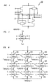
- FIG. 6 illustrates a NOR switching array 600 that employs current recycling according to an exemplary embodiment of the present invention.
- the corresponding block representation of the array is shown in Figure 7.
- current Is1 provided from circuitry such as is shown in Figures 3 and 4 or another NOR switching array or a current source may be utilized to drive the desired outputs C and C in response to the inputs A, A , B, or B .
- Figure 8 is a block diagram illustrating a low noise logic block using current recycling.
- the low noise logic block is a three tier Boolean circuit. Signals from the same tier can be sent to any logic gate in the same tier. An impedance (not shown) is placed at the output of each gate to insure a continuous circuit. Signals sent between tiers may be level shifted to account for a voltage shift between arrays.
- the NAND array 925, the NOR array 905, and the AOI array 940 receive current I from a current source or current from a previous circuit stage such as a line diver.
- the rerouted current I reroutedx from each array 905, 930, 925, 915, 940, 920 are provided to a respective subsequent array.
- the rerouted current I rerouted7 from arrays 910, 935, 945 are provided to other circuitry or to ground.
- the NOR arrays 905, 910, 915, and 920 may be formed using the circuitry shown in Figure 6.
- the circuitry shown in Figure 6 may also be used to form NAND array 925. In this case circuitry is provided to reverse the polarity of the inputs to the NOR array making the circuitry perform as a NAND gate.
- the remaining components including the Exclusive OR (EXOR) arrays 930 and 935, the AND-OR-INVERT (AOI) array 940, and OR-AND-INVERT (OAI) array 945 each may be formed using conventional circuitry except that the circuits are modified to receive current from another circuit or provide current to another circuit according to the present invention.
- Inputs A through L represent digital inputs into the NOR switching array.
- additional circuitry may be added to, for example, the line drivers without increasing or without significantly increasing the power consumption of the driver. In this way, complex functions may be included in the line drivers. Further, this may potentially lower the propagation delay of the cell.
- an output buffer may include a line driver and some other circuitry for performing some function.
- the line driver and the other circuitry would be interconnected so that current from the line driver may be provided to the other circuitry or the current from the other circuitry may be provided to the line driver.
- the present invention provides circuitry that performs one operation and passes current to other circuitry so that it can perform another operation. Therefore, the invention should not be limited to the specific circuits shown herein.
Landscapes
- Physics & Mathematics (AREA)
- Engineering & Computer Science (AREA)
- Computer Hardware Design (AREA)
- Computing Systems (AREA)
- General Engineering & Computer Science (AREA)
- Mathematical Physics (AREA)
- Logic Circuits (AREA)
- Dc Digital Transmission (AREA)
Applications Claiming Priority (2)
| Application Number | Priority Date | Filing Date | Title |
|---|---|---|---|
| US09/648,162 US6552581B1 (en) | 2000-08-25 | 2000-08-25 | Current recycling circuit and a method of current recycling |
| US648162 | 2000-08-25 |
Publications (2)
| Publication Number | Publication Date |
|---|---|
| EP1184986A1 EP1184986A1 (en) | 2002-03-06 |
| EP1184986B1 true EP1184986B1 (en) | 2004-10-20 |
Family
ID=24599682
Family Applications (1)
| Application Number | Title | Priority Date | Filing Date |
|---|---|---|---|
| EP20010307196 Expired - Lifetime EP1184986B1 (en) | 2000-08-25 | 2001-08-23 | LVDS circuits connected in series for the supply current |
Country Status (4)
| Country | Link |
|---|---|
| US (1) | US6552581B1 (cg-RX-API-DMAC7.html) |
| EP (1) | EP1184986B1 (cg-RX-API-DMAC7.html) |
| JP (1) | JP4019168B2 (cg-RX-API-DMAC7.html) |
| DE (1) | DE60106541T2 (cg-RX-API-DMAC7.html) |
Cited By (1)
| Publication number | Priority date | Publication date | Assignee | Title |
|---|---|---|---|---|
| US7683673B2 (en) | 2007-04-24 | 2010-03-23 | National Semiconductor Corporation | Stacked differential signal transmission circuitry |
Families Citing this family (45)
| Publication number | Priority date | Publication date | Assignee | Title |
|---|---|---|---|---|
| US7355358B2 (en) * | 2003-10-23 | 2008-04-08 | Hewlett-Packard Development Company, L.P. | Configurable H-bridge circuit |
| US7342420B2 (en) * | 2004-09-24 | 2008-03-11 | Integrated Device Technology, Inc. | Low power output driver |
| US7215173B2 (en) * | 2005-01-31 | 2007-05-08 | Intel Corporation | Low-swing level shifter |
| TWI309101B (en) * | 2005-08-16 | 2009-04-21 | Realtek Semiconductor Corp | Voltage converting circuit, voltage converting apparatus, and related circuit systems |
| US7411431B2 (en) * | 2006-02-06 | 2008-08-12 | Fairchild Semiconductor Corporation | Dual output differential line driver using single current |
| US7551006B2 (en) * | 2007-10-04 | 2009-06-23 | International Business Machines Corporation | Low voltage differential signalling driver |
| JP5420847B2 (ja) * | 2008-02-19 | 2014-02-19 | ピーエスフォー ルクスコ エスエイアールエル | 信号伝送回路及びこれを用いた信号伝送システム |
| US20110035540A1 (en) * | 2009-08-10 | 2011-02-10 | Adtron, Inc. | Flash blade system architecture and method |
| US8169257B2 (en) * | 2009-11-18 | 2012-05-01 | Freescale Semiconductor, Inc. | System and method for communicating between multiple voltage tiers |
| US8476962B2 (en) * | 2009-11-18 | 2013-07-02 | Freescale Semiconductor, Inc. | System having multiple voltage tiers and method therefor |
| US8909851B2 (en) | 2011-02-08 | 2014-12-09 | SMART Storage Systems, Inc. | Storage control system with change logging mechanism and method of operation thereof |
| US8368426B2 (en) * | 2011-02-24 | 2013-02-05 | Via Technologies, Inc. | Low voltage differential signal driving circuit and digital signal transmitter |
| US8952725B2 (en) | 2011-02-24 | 2015-02-10 | Via Technologies, Inc. | Low voltage differential signal driving circuit and electronic device compatible with wired transmission |
| US8935466B2 (en) | 2011-03-28 | 2015-01-13 | SMART Storage Systems, Inc. | Data storage system with non-volatile memory and method of operation thereof |
| US9098399B2 (en) | 2011-08-31 | 2015-08-04 | SMART Storage Systems, Inc. | Electronic system with storage management mechanism and method of operation thereof |
| US9021319B2 (en) | 2011-09-02 | 2015-04-28 | SMART Storage Systems, Inc. | Non-volatile memory management system with load leveling and method of operation thereof |
| US9021231B2 (en) | 2011-09-02 | 2015-04-28 | SMART Storage Systems, Inc. | Storage control system with write amplification control mechanism and method of operation thereof |
| US9063844B2 (en) | 2011-09-02 | 2015-06-23 | SMART Storage Systems, Inc. | Non-volatile memory management system with time measure mechanism and method of operation thereof |
| US20130132623A1 (en) * | 2011-11-17 | 2013-05-23 | Velocio Networks, Inc. | Method for Interconnecting Modules for High Speed Bidirectional Communications |
| US9239781B2 (en) | 2012-02-07 | 2016-01-19 | SMART Storage Systems, Inc. | Storage control system with erase block mechanism and method of operation thereof |
| US9298252B2 (en) | 2012-04-17 | 2016-03-29 | SMART Storage Systems, Inc. | Storage control system with power down mechanism and method of operation thereof |
| US8949689B2 (en) | 2012-06-11 | 2015-02-03 | SMART Storage Systems, Inc. | Storage control system with data management mechanism and method of operation thereof |
| US9671962B2 (en) | 2012-11-30 | 2017-06-06 | Sandisk Technologies Llc | Storage control system with data management mechanism of parity and method of operation thereof |
| US9123445B2 (en) | 2013-01-22 | 2015-09-01 | SMART Storage Systems, Inc. | Storage control system with data management mechanism and method of operation thereof |
| US9214965B2 (en) | 2013-02-20 | 2015-12-15 | Sandisk Enterprise Ip Llc | Method and system for improving data integrity in non-volatile storage |
| US9329928B2 (en) | 2013-02-20 | 2016-05-03 | Sandisk Enterprise IP LLC. | Bandwidth optimization in a non-volatile memory system |
| US9183137B2 (en) | 2013-02-27 | 2015-11-10 | SMART Storage Systems, Inc. | Storage control system with data management mechanism and method of operation thereof |
| US9470720B2 (en) | 2013-03-08 | 2016-10-18 | Sandisk Technologies Llc | Test system with localized heating and method of manufacture thereof |
| US9043780B2 (en) | 2013-03-27 | 2015-05-26 | SMART Storage Systems, Inc. | Electronic system with system modification control mechanism and method of operation thereof |
| US10049037B2 (en) | 2013-04-05 | 2018-08-14 | Sandisk Enterprise Ip Llc | Data management in a storage system |
| US9170941B2 (en) | 2013-04-05 | 2015-10-27 | Sandisk Enterprises IP LLC | Data hardening in a storage system |
| US9543025B2 (en) | 2013-04-11 | 2017-01-10 | Sandisk Technologies Llc | Storage control system with power-off time estimation mechanism and method of operation thereof |
| US10546648B2 (en) | 2013-04-12 | 2020-01-28 | Sandisk Technologies Llc | Storage control system with data management mechanism and method of operation thereof |
| US9898056B2 (en) | 2013-06-19 | 2018-02-20 | Sandisk Technologies Llc | Electronic assembly with thermal channel and method of manufacture thereof |
| US9313874B2 (en) | 2013-06-19 | 2016-04-12 | SMART Storage Systems, Inc. | Electronic system with heat extraction and method of manufacture thereof |
| US9367353B1 (en) | 2013-06-25 | 2016-06-14 | Sandisk Technologies Inc. | Storage control system with power throttling mechanism and method of operation thereof |
| US9244519B1 (en) | 2013-06-25 | 2016-01-26 | Smart Storage Systems. Inc. | Storage system with data transfer rate adjustment for power throttling |
| US9146850B2 (en) | 2013-08-01 | 2015-09-29 | SMART Storage Systems, Inc. | Data storage system with dynamic read threshold mechanism and method of operation thereof |
| US9361222B2 (en) | 2013-08-07 | 2016-06-07 | SMART Storage Systems, Inc. | Electronic system with storage drive life estimation mechanism and method of operation thereof |
| US9448946B2 (en) | 2013-08-07 | 2016-09-20 | Sandisk Technologies Llc | Data storage system with stale data mechanism and method of operation thereof |
| US9431113B2 (en) | 2013-08-07 | 2016-08-30 | Sandisk Technologies Llc | Data storage system with dynamic erase block grouping mechanism and method of operation thereof |
| US9152555B2 (en) | 2013-11-15 | 2015-10-06 | Sandisk Enterprise IP LLC. | Data management with modular erase in a data storage system |
| US12021029B2 (en) | 2022-02-16 | 2024-06-25 | Zetagig Inc. | Systems, methods, and apparatuses for an array of devices |
| US12046601B2 (en) | 2022-02-16 | 2024-07-23 | Zetagig Inc. | Apparatuses, methods, and systems for an array of devices |
| US11953963B2 (en) * | 2022-02-16 | 2024-04-09 | Zetagig Inc. | Apparatuses and methods for an array of devices |
Citations (1)
| Publication number | Priority date | Publication date | Assignee | Title |
|---|---|---|---|---|
| EP0310359A2 (en) * | 1987-09-29 | 1989-04-05 | Kabushiki Kaisha Toshiba | Logic circuit using Schottky barrier FETs |
Family Cites Families (11)
| Publication number | Priority date | Publication date | Assignee | Title |
|---|---|---|---|---|
| JPS58210722A (ja) | 1982-06-02 | 1983-12-08 | Hitachi Ltd | 半導体集積回路 |
| US5032745A (en) * | 1989-02-22 | 1991-07-16 | National Semiconductor Corporation | Current sensing of DC or a stepper motor |
| KR920010346B1 (ko) * | 1990-05-23 | 1992-11-27 | 삼성전자 주식회사 | 반도체 메모리의 센스앰프 구동회로 |
| JP2806050B2 (ja) * | 1991-02-06 | 1998-09-30 | 日本電気株式会社 | 電源回路 |
| JP3525195B2 (ja) * | 1994-08-02 | 2004-05-10 | 光洋精工株式会社 | 電動パワーステアリング装置 |
| FR2731570B1 (fr) * | 1995-03-07 | 1997-05-23 | Sgs Thomson Microelectronics | Circuit logique a etage differentiel |
| US5867057A (en) * | 1996-02-02 | 1999-02-02 | United Microelectronics Corp. | Apparatus and method for generating bias voltages for liquid crystal display |
| US5708389A (en) * | 1996-03-15 | 1998-01-13 | Lucent Technologies Inc. | Integrated circuit employing quantized feedback |
| JPH09261038A (ja) | 1996-03-22 | 1997-10-03 | Nec Corp | 論理回路 |
| US5977796A (en) | 1997-06-26 | 1999-11-02 | Lucent Technologies, Inc. | Low voltage differential swing interconnect buffer circuit |
| US6154044A (en) * | 1998-11-20 | 2000-11-28 | Trw Inc. | Superconductive logic gate and random access memory |
-
2000
- 2000-08-25 US US09/648,162 patent/US6552581B1/en not_active Expired - Lifetime
-
2001
- 2001-08-23 EP EP20010307196 patent/EP1184986B1/en not_active Expired - Lifetime
- 2001-08-23 DE DE2001606541 patent/DE60106541T2/de not_active Expired - Lifetime
- 2001-08-24 JP JP2001253858A patent/JP4019168B2/ja not_active Expired - Fee Related
Patent Citations (1)
| Publication number | Priority date | Publication date | Assignee | Title |
|---|---|---|---|---|
| EP0310359A2 (en) * | 1987-09-29 | 1989-04-05 | Kabushiki Kaisha Toshiba | Logic circuit using Schottky barrier FETs |
Cited By (2)
| Publication number | Priority date | Publication date | Assignee | Title |
|---|---|---|---|---|
| US7683673B2 (en) | 2007-04-24 | 2010-03-23 | National Semiconductor Corporation | Stacked differential signal transmission circuitry |
| TWI400916B (zh) * | 2007-04-24 | 2013-07-01 | Nat Semiconductor Corp | 堆疊式差動信號傳輸電路 |
Also Published As
| Publication number | Publication date |
|---|---|
| US6552581B1 (en) | 2003-04-22 |
| EP1184986A1 (en) | 2002-03-06 |
| DE60106541D1 (de) | 2004-11-25 |
| DE60106541T2 (de) | 2005-10-13 |
| JP4019168B2 (ja) | 2007-12-12 |
| JP2002111478A (ja) | 2002-04-12 |
Similar Documents
| Publication | Publication Date | Title |
|---|---|---|
| EP1184986B1 (en) | LVDS circuits connected in series for the supply current | |
| US5568077A (en) | Latch circuit | |
| US7868790B2 (en) | Single ended pseudo differential interconnection circuit and single ended pseudo differential signaling method | |
| JP3590557B2 (ja) | レベルシフタを有する半導体装置のデータ出力回路及びデータ出力方法、該データ出力回路を有する半導体装置 | |
| JP4814791B2 (ja) | レベル・シフター | |
| US6498514B2 (en) | Domino circuit | |
| JPH09214314A (ja) | ドライバ回路装置 | |
| US5986489A (en) | Slew rate control circuit for an integrated circuit | |
| JPH0334719A (ja) | 半導体集積回路 | |
| US6111455A (en) | Method for controlling delays in silicon on insulator circuits | |
| CA2201853A1 (en) | High voltage level shifter for switching high voltage in non-volatile memory integrated circuits | |
| JP3759121B2 (ja) | 半導体装置 | |
| EP0823786A2 (en) | Pseudo differential bus driver/receiver for field programmable devices | |
| US6847225B2 (en) | CML (current mode logic) OCD (off chip driver)—ODT (on die termination) circuit for bidirectional data transmission | |
| US6762625B1 (en) | Programmable differential current mode line driver with multiple classes of circuit operation | |
| JP2000059199A (ja) | 出力バッファ及びそのバッファリング方法 | |
| US5517186A (en) | EPROM-based crossbar switch with zero standby power | |
| WO1998006177A9 (en) | Combined logic gate and latch | |
| JP3143750B2 (ja) | クロック回路 | |
| WO1998006177A1 (en) | Combined logic gate and latch | |
| US20030058001A1 (en) | Fast, symmetrical XOR/XNOR gate | |
| KR20040010206A (ko) | 버스 인터페이스 회로 및 리시버 회로 | |
| US7449940B2 (en) | Buffer circuit | |
| KR100428818B1 (ko) | 출력버퍼회로 | |
| US5495182A (en) | Fast-fully restoring polarity control circuit |
Legal Events
| Date | Code | Title | Description |
|---|---|---|---|
| PUAI | Public reference made under article 153(3) epc to a published international application that has entered the european phase |
Free format text: ORIGINAL CODE: 0009012 |
|
| AK | Designated contracting states |
Kind code of ref document: A1 Designated state(s): AT BE CH CY DE DK ES FI FR GB GR IE IT LI LU MC NL PT SE TR Kind code of ref document: A1 Designated state(s): DE GB |
|
| AX | Request for extension of the european patent |
Free format text: AL;LT;LV;MK;RO;SI |
|
| 17P | Request for examination filed |
Effective date: 20020906 |
|
| AKX | Designation fees paid |
Free format text: DE GB |
|
| 17Q | First examination report despatched |
Effective date: 20021025 |
|
| GRAH | Despatch of communication of intention to grant a patent |
Free format text: ORIGINAL CODE: EPIDOS IGRA |
|
| GRAS | Grant fee paid |
Free format text: ORIGINAL CODE: EPIDOSNIGR3 |
|
| GRAA | (expected) grant |
Free format text: ORIGINAL CODE: 0009210 |
|
| AK | Designated contracting states |
Kind code of ref document: B1 Designated state(s): DE GB |
|
| REG | Reference to a national code |
Ref country code: GB Ref legal event code: FG4D |
|
| REG | Reference to a national code |
Ref country code: IE Ref legal event code: FG4D |
|
| REF | Corresponds to: |
Ref document number: 60106541 Country of ref document: DE Date of ref document: 20041125 Kind code of ref document: P |
|
| PLBE | No opposition filed within time limit |
Free format text: ORIGINAL CODE: 0009261 |
|
| STAA | Information on the status of an ep patent application or granted ep patent |
Free format text: STATUS: NO OPPOSITION FILED WITHIN TIME LIMIT |
|
| 26N | No opposition filed |
Effective date: 20050721 |
|
| PGFP | Annual fee paid to national office [announced via postgrant information from national office to epo] |
Ref country code: DE Payment date: 20140821 Year of fee payment: 14 |
|
| PGFP | Annual fee paid to national office [announced via postgrant information from national office to epo] |
Ref country code: GB Payment date: 20140820 Year of fee payment: 14 |
|
| REG | Reference to a national code |
Ref country code: DE Ref legal event code: R082 Ref document number: 60106541 Country of ref document: DE Representative=s name: DILG HAEUSLER SCHINDELMANN PATENTANWALTSGESELL, DE |
|
| REG | Reference to a national code |
Ref country code: DE Ref legal event code: R119 Ref document number: 60106541 Country of ref document: DE |
|
| GBPC | Gb: european patent ceased through non-payment of renewal fee |
Effective date: 20150823 |
|
| PG25 | Lapsed in a contracting state [announced via postgrant information from national office to epo] |
Ref country code: GB Free format text: LAPSE BECAUSE OF NON-PAYMENT OF DUE FEES Effective date: 20150823 Ref country code: DE Free format text: LAPSE BECAUSE OF NON-PAYMENT OF DUE FEES Effective date: 20160301 |