EP1184913A1 - Nitride semiconductor device and its manufacturino method - Google Patents
Nitride semiconductor device and its manufacturino method Download PDFInfo
- Publication number
- EP1184913A1 EP1184913A1 EP00902126A EP00902126A EP1184913A1 EP 1184913 A1 EP1184913 A1 EP 1184913A1 EP 00902126 A EP00902126 A EP 00902126A EP 00902126 A EP00902126 A EP 00902126A EP 1184913 A1 EP1184913 A1 EP 1184913A1
- Authority
- EP
- European Patent Office
- Prior art keywords
- layer
- gan
- nitride semiconductor
- substrate
- forming
- Prior art date
- Legal status (The legal status is an assumption and is not a legal conclusion. Google has not performed a legal analysis and makes no representation as to the accuracy of the status listed.)
- Granted
Links
Images


Classifications
-
- C—CHEMISTRY; METALLURGY
- C30—CRYSTAL GROWTH
- C30B—SINGLE-CRYSTAL GROWTH; UNIDIRECTIONAL SOLIDIFICATION OF EUTECTIC MATERIAL OR UNIDIRECTIONAL DEMIXING OF EUTECTOID MATERIAL; REFINING BY ZONE-MELTING OF MATERIAL; PRODUCTION OF A HOMOGENEOUS POLYCRYSTALLINE MATERIAL WITH DEFINED STRUCTURE; SINGLE CRYSTALS OR HOMOGENEOUS POLYCRYSTALLINE MATERIAL WITH DEFINED STRUCTURE; AFTER-TREATMENT OF SINGLE CRYSTALS OR A HOMOGENEOUS POLYCRYSTALLINE MATERIAL WITH DEFINED STRUCTURE; APPARATUS THEREFOR
- C30B29/00—Single crystals or homogeneous polycrystalline material with defined structure characterised by the material or by their shape
- C30B29/10—Inorganic compounds or compositions
- C30B29/40—AIIIBV compounds wherein A is B, Al, Ga, In or Tl and B is N, P, As, Sb or Bi
- C30B29/403—AIII-nitrides
-
- C—CHEMISTRY; METALLURGY
- C30—CRYSTAL GROWTH
- C30B—SINGLE-CRYSTAL GROWTH; UNIDIRECTIONAL SOLIDIFICATION OF EUTECTIC MATERIAL OR UNIDIRECTIONAL DEMIXING OF EUTECTOID MATERIAL; REFINING BY ZONE-MELTING OF MATERIAL; PRODUCTION OF A HOMOGENEOUS POLYCRYSTALLINE MATERIAL WITH DEFINED STRUCTURE; SINGLE CRYSTALS OR HOMOGENEOUS POLYCRYSTALLINE MATERIAL WITH DEFINED STRUCTURE; AFTER-TREATMENT OF SINGLE CRYSTALS OR A HOMOGENEOUS POLYCRYSTALLINE MATERIAL WITH DEFINED STRUCTURE; APPARATUS THEREFOR
- C30B25/00—Single-crystal growth by chemical reaction of reactive gases, e.g. chemical vapour-deposition growth
- C30B25/02—Epitaxial-layer growth
- C30B25/18—Epitaxial-layer growth characterised by the substrate
- C30B25/20—Epitaxial-layer growth characterised by the substrate the substrate being of the same materials as the epitaxial layer
-
- H—ELECTRICITY
- H01—ELECTRIC ELEMENTS
- H01S—DEVICES USING THE PROCESS OF LIGHT AMPLIFICATION BY STIMULATED EMISSION OF RADIATION [LASER] TO AMPLIFY OR GENERATE LIGHT; DEVICES USING STIMULATED EMISSION OF ELECTROMAGNETIC RADIATION IN WAVE RANGES OTHER THAN OPTICAL
- H01S5/00—Semiconductor lasers
- H01S5/04—Processes or apparatus for excitation, e.g. pumping, e.g. by electron beams
- H01S5/042—Electrical excitation ; Circuits therefor
- H01S5/0421—Electrical excitation ; Circuits therefor characterised by the semiconducting contacting layers
-
- H—ELECTRICITY
- H01—ELECTRIC ELEMENTS
- H01S—DEVICES USING THE PROCESS OF LIGHT AMPLIFICATION BY STIMULATED EMISSION OF RADIATION [LASER] TO AMPLIFY OR GENERATE LIGHT; DEVICES USING STIMULATED EMISSION OF ELECTROMAGNETIC RADIATION IN WAVE RANGES OTHER THAN OPTICAL
- H01S5/00—Semiconductor lasers
- H01S5/30—Structure or shape of the active region; Materials used for the active region
- H01S5/32—Structure or shape of the active region; Materials used for the active region comprising PN junctions, e.g. hetero- or double- heterostructures
- H01S5/323—Structure or shape of the active region; Materials used for the active region comprising PN junctions, e.g. hetero- or double- heterostructures in AIIIBV compounds, e.g. AlGaAs-laser, InP-based laser
- H01S5/32308—Structure or shape of the active region; Materials used for the active region comprising PN junctions, e.g. hetero- or double- heterostructures in AIIIBV compounds, e.g. AlGaAs-laser, InP-based laser emitting light at a wavelength less than 900 nm
- H01S5/32341—Structure or shape of the active region; Materials used for the active region comprising PN junctions, e.g. hetero- or double- heterostructures in AIIIBV compounds, e.g. AlGaAs-laser, InP-based laser emitting light at a wavelength less than 900 nm blue laser based on GaN or GaP
-
- H—ELECTRICITY
- H10—SEMICONDUCTOR DEVICES; ELECTRIC SOLID-STATE DEVICES NOT OTHERWISE PROVIDED FOR
- H10H—INORGANIC LIGHT-EMITTING SEMICONDUCTOR DEVICES HAVING POTENTIAL BARRIERS
- H10H20/00—Individual inorganic light-emitting semiconductor devices having potential barriers, e.g. light-emitting diodes [LED]
- H10H20/01—Manufacture or treatment
- H10H20/011—Manufacture or treatment of bodies, e.g. forming semiconductor layers
- H10H20/013—Manufacture or treatment of bodies, e.g. forming semiconductor layers having light-emitting regions comprising only Group III-V materials
- H10H20/0137—Manufacture or treatment of bodies, e.g. forming semiconductor layers having light-emitting regions comprising only Group III-V materials the light-emitting regions comprising nitride materials
-
- H—ELECTRICITY
- H10—SEMICONDUCTOR DEVICES; ELECTRIC SOLID-STATE DEVICES NOT OTHERWISE PROVIDED FOR
- H10P—GENERIC PROCESSES OR APPARATUS FOR THE MANUFACTURE OR TREATMENT OF DEVICES COVERED BY CLASS H10
- H10P14/00—Formation of materials, e.g. in the shape of layers or pillars
- H10P14/20—Formation of materials, e.g. in the shape of layers or pillars of semiconductor materials
- H10P14/29—Formation of materials, e.g. in the shape of layers or pillars of semiconductor materials characterised by the substrates
- H10P14/2901—Materials
- H10P14/2902—Materials being Group IVA materials
- H10P14/2904—Silicon carbide
-
- H—ELECTRICITY
- H10—SEMICONDUCTOR DEVICES; ELECTRIC SOLID-STATE DEVICES NOT OTHERWISE PROVIDED FOR
- H10P—GENERIC PROCESSES OR APPARATUS FOR THE MANUFACTURE OR TREATMENT OF DEVICES COVERED BY CLASS H10
- H10P14/00—Formation of materials, e.g. in the shape of layers or pillars
- H10P14/20—Formation of materials, e.g. in the shape of layers or pillars of semiconductor materials
- H10P14/29—Formation of materials, e.g. in the shape of layers or pillars of semiconductor materials characterised by the substrates
- H10P14/2901—Materials
- H10P14/2921—Materials being crystalline insulating materials
-
- H—ELECTRICITY
- H10—SEMICONDUCTOR DEVICES; ELECTRIC SOLID-STATE DEVICES NOT OTHERWISE PROVIDED FOR
- H10P—GENERIC PROCESSES OR APPARATUS FOR THE MANUFACTURE OR TREATMENT OF DEVICES COVERED BY CLASS H10
- H10P14/00—Formation of materials, e.g. in the shape of layers or pillars
- H10P14/20—Formation of materials, e.g. in the shape of layers or pillars of semiconductor materials
- H10P14/29—Formation of materials, e.g. in the shape of layers or pillars of semiconductor materials characterised by the substrates
- H10P14/2924—Structures
- H10P14/2925—Surface structures
-
- H—ELECTRICITY
- H10—SEMICONDUCTOR DEVICES; ELECTRIC SOLID-STATE DEVICES NOT OTHERWISE PROVIDED FOR
- H10P—GENERIC PROCESSES OR APPARATUS FOR THE MANUFACTURE OR TREATMENT OF DEVICES COVERED BY CLASS H10
- H10P14/00—Formation of materials, e.g. in the shape of layers or pillars
- H10P14/20—Formation of materials, e.g. in the shape of layers or pillars of semiconductor materials
- H10P14/32—Formation of materials, e.g. in the shape of layers or pillars of semiconductor materials characterised by intermediate layers between substrates and deposited layers
- H10P14/3202—Materials thereof
- H10P14/3214—Materials thereof being Group IIIA-VA semiconductors
- H10P14/3216—Nitrides
-
- H—ELECTRICITY
- H10—SEMICONDUCTOR DEVICES; ELECTRIC SOLID-STATE DEVICES NOT OTHERWISE PROVIDED FOR
- H10P—GENERIC PROCESSES OR APPARATUS FOR THE MANUFACTURE OR TREATMENT OF DEVICES COVERED BY CLASS H10
- H10P14/00—Formation of materials, e.g. in the shape of layers or pillars
- H10P14/20—Formation of materials, e.g. in the shape of layers or pillars of semiconductor materials
- H10P14/34—Deposited materials, e.g. layers
- H10P14/3402—Deposited materials, e.g. layers characterised by the chemical composition
- H10P14/3414—Deposited materials, e.g. layers characterised by the chemical composition being group IIIA-VIA materials
- H10P14/3416—Nitrides
-
- H—ELECTRICITY
- H01—ELECTRIC ELEMENTS
- H01S—DEVICES USING THE PROCESS OF LIGHT AMPLIFICATION BY STIMULATED EMISSION OF RADIATION [LASER] TO AMPLIFY OR GENERATE LIGHT; DEVICES USING STIMULATED EMISSION OF ELECTROMAGNETIC RADIATION IN WAVE RANGES OTHER THAN OPTICAL
- H01S2301/00—Functional characteristics
- H01S2301/17—Semiconductor lasers comprising special layers
- H01S2301/173—The laser chip comprising special buffer layers, e.g. dislocation prevention or reduction
-
- H—ELECTRICITY
- H01—ELECTRIC ELEMENTS
- H01S—DEVICES USING THE PROCESS OF LIGHT AMPLIFICATION BY STIMULATED EMISSION OF RADIATION [LASER] TO AMPLIFY OR GENERATE LIGHT; DEVICES USING STIMULATED EMISSION OF ELECTROMAGNETIC RADIATION IN WAVE RANGES OTHER THAN OPTICAL
- H01S2304/00—Special growth methods for semiconductor lasers
- H01S2304/04—MOCVD or MOVPE
-
- H—ELECTRICITY
- H01—ELECTRIC ELEMENTS
- H01S—DEVICES USING THE PROCESS OF LIGHT AMPLIFICATION BY STIMULATED EMISSION OF RADIATION [LASER] TO AMPLIFY OR GENERATE LIGHT; DEVICES USING STIMULATED EMISSION OF ELECTROMAGNETIC RADIATION IN WAVE RANGES OTHER THAN OPTICAL
- H01S5/00—Semiconductor lasers
- H01S5/02—Structural details or components not essential to laser action
- H01S5/0206—Substrates, e.g. growth, shape, material, removal or bonding
- H01S5/021—Silicon based substrates
-
- H—ELECTRICITY
- H01—ELECTRIC ELEMENTS
- H01S—DEVICES USING THE PROCESS OF LIGHT AMPLIFICATION BY STIMULATED EMISSION OF RADIATION [LASER] TO AMPLIFY OR GENERATE LIGHT; DEVICES USING STIMULATED EMISSION OF ELECTROMAGNETIC RADIATION IN WAVE RANGES OTHER THAN OPTICAL
- H01S5/00—Semiconductor lasers
- H01S5/04—Processes or apparatus for excitation, e.g. pumping, e.g. by electron beams
- H01S5/042—Electrical excitation ; Circuits therefor
- H01S5/0421—Electrical excitation ; Circuits therefor characterised by the semiconducting contacting layers
- H01S5/0422—Electrical excitation ; Circuits therefor characterised by the semiconducting contacting layers with n- and p-contacts on the same side of the active layer
-
- H—ELECTRICITY
- H01—ELECTRIC ELEMENTS
- H01S—DEVICES USING THE PROCESS OF LIGHT AMPLIFICATION BY STIMULATED EMISSION OF RADIATION [LASER] TO AMPLIFY OR GENERATE LIGHT; DEVICES USING STIMULATED EMISSION OF ELECTROMAGNETIC RADIATION IN WAVE RANGES OTHER THAN OPTICAL
- H01S5/00—Semiconductor lasers
- H01S5/30—Structure or shape of the active region; Materials used for the active region
- H01S5/32—Structure or shape of the active region; Materials used for the active region comprising PN junctions, e.g. hetero- or double- heterostructures
- H01S5/3201—Structure or shape of the active region; Materials used for the active region comprising PN junctions, e.g. hetero- or double- heterostructures incorporating bulkstrain effects, e.g. strain compensation, strain related to polarisation
-
- H—ELECTRICITY
- H10—SEMICONDUCTOR DEVICES; ELECTRIC SOLID-STATE DEVICES NOT OTHERWISE PROVIDED FOR
- H10P—GENERIC PROCESSES OR APPARATUS FOR THE MANUFACTURE OR TREATMENT OF DEVICES COVERED BY CLASS H10
- H10P14/00—Formation of materials, e.g. in the shape of layers or pillars
- H10P14/20—Formation of materials, e.g. in the shape of layers or pillars of semiconductor materials
- H10P14/24—Formation of materials, e.g. in the shape of layers or pillars of semiconductor materials using chemical vapour deposition [CVD]
-
- H—ELECTRICITY
- H10—SEMICONDUCTOR DEVICES; ELECTRIC SOLID-STATE DEVICES NOT OTHERWISE PROVIDED FOR
- H10P—GENERIC PROCESSES OR APPARATUS FOR THE MANUFACTURE OR TREATMENT OF DEVICES COVERED BY CLASS H10
- H10P14/00—Formation of materials, e.g. in the shape of layers or pillars
- H10P14/20—Formation of materials, e.g. in the shape of layers or pillars of semiconductor materials
- H10P14/27—Formation of materials, e.g. in the shape of layers or pillars of semiconductor materials using selective deposition, e.g. simultaneous growth of monocrystalline and non-monocrystalline semiconductor materials
- H10P14/271—Formation of materials, e.g. in the shape of layers or pillars of semiconductor materials using selective deposition, e.g. simultaneous growth of monocrystalline and non-monocrystalline semiconductor materials characterised by the preparation of substrate for selective deposition
Definitions
- This invention relates to a device provided with a nitride semiconductor (In x Al y Ga 1-x-y N, 0 ⁇ x, 0 ⁇ y, x+y ⁇ 1) including light emitting diode (LED), laser diode (LD), or other electronic devices and power devices.
- a nitride semiconductor In x Al y Ga 1-x-y N, 0 ⁇ x, 0 ⁇ y, x+y ⁇ 1
- LED light emitting diode
- LD laser diode
- the present invention relates to a prevention of a small cracking in nitride semiconductor layers, which occurs in the nitride semiconductor device using a GaN substrate.
- Blue LEDs using nitride semiconductors have already been provided for practical use. Recently, it becomes possible to provide a practical blue laser diode made of nitride semiconductor by using a GaN substrate.
- the inventors have disclosed a nitride semiconductor laser diode using a GaN substrate in, for example, Japanese Journal of Applied Physics. Vol.37(1998) pp.L309-L312.
- the GaN substrate can be formed, for example, by the following method: A GaN layer is formed on a sapphire substrate and a protective film made of SiO 2 is formed partially on the surface of the GaN film. Then, GaN is grown again on the GaN film and the sapphire substrate is removed. The secondly-formed GaN layer grows mainly in a lateral direction, so that a proceeding of dislocations is prevented. By using this method, a GaN substrate having low dislocation density can be obtained.
- the nitride semiconductor laser device made with such a low dislocation-density GaN substrate showed continuous-wave oscillation and can be operated continuously for more than ten thousand hours.
- the nitride semiconductor laser diode with lifetime of more than ten thousand hours can be applied for practical use. However, in some applications, much longer lifetime is desired.
- the inventors examined the nitride semiconductor laser device obtained by the above-described method and found that extremely small cracks tend to occur in the nitride semiconductor layers grown on the GaN substrate, particularly in the n-type GaN contact layer which is grown directly on the GaN substrate.
- the crack is too small to observe by a typical optical microscope, however, it can be observed by a fluorescence microscope. It is a surprising fact that small cracks tend to occur in the GaN layer which is directly grown on the same-composition GaN substrate.
- the occurrence of small cracks is a specific phenomenon for the GaN substrate which is manufactured by the lateral-growth method.
- small cracks occur for an unknown reason. In any case, it is probable that the small cracks cause an increase of thresholds and a deterioration of lifetime of the laser device.
- the small cracks may also cause a decrease in reliability for other nitride semiconductor devices, as well as in the laser device.
- the object of the present invention is to reduce extremely small cracks in the nitride semiconductor layers and to extend a lifetime of the nitride semiconductor device using a GaN substrate, thus improving a reliability of the nitride semiconductor device.
- the compressive strain may be achieved by forming a device-forming layer having a smaller coefficient of thermal expansion than that of GaN directly on the GaN substrate.
- the device-forming layer directly grown on the GaN substrate is preferably Al a Ga 1-a N, (0 ⁇ a ⁇ 1). Because Al a Ga 1-a N, (0 ⁇ a ⁇ 1) has a smaller coefficient of thermal expansion than that of GaN and can be grown on the GaN substrate as a good crystalline.
- the device structure constructed by the device-forming layers preferably comprises an n-type cladding layer containing Al, an active layer containing InGaN and a p-type cladding layer containing Al. Employing this structure together with the cracks-reducing structure, a good-characteristics device is provided.
- the device-forming layer directly grown on the GaN substrate may play various kinds of rolls according to the device structure.
- the layer may be an buffer layer for preventing small cracks, or an n-contact layer.
- the layer may be an n-clad layer.
- the GaN substrate is preferably manufactured by using the lateral-growth method.
- the laterally grown GaN substrate not only the occurrence of the small cracks but also a propagation of dislocations is prevented.
- a nitride semiconductor device having good characteristics is provided.
- the manufacturing method of the nitride semiconductor element of the present invention comprises the steps of:
- the auxiliary substrate may be removed from the GaN substrate after forming the single-crystal GaN layer.
- a thermal expansion coefficient of the nitride layer contacting on the GaN substrate is preferably smaller than that of GaN so as to provide the compressive strain in the nitride semiconductor layer.
- the compressive strain prevents formation of small cracks in the nitride semiconductor layers.
- the relation of coefficients of thermal expansion is ⁇ 1 ⁇ ⁇ 2 and a tensile strain is laid in the in-plane direction on the GaN layer grown on the SiC substrate.
- the relation of coefficients of thermal expansion is ⁇ 2 ⁇ ⁇ 3 and a compressive strain is laid in the in-plane direction on the GaN layer grown on the sapphire substrate.
- the liability of cracks to occur depends on whether the strain laid on the layer is a tensile strain or a compressive strain.
- GaN substrate refers to a substrate having a low-dislocation-density single-crystal GaN layer on its surface.
- the GaN substrate may be composed only of a single-crystal GaN layer, or it may be composed of an auxiliary substrate made of different material from nitride semiconductor such as sapphire or SiC and a low-dislocation-density single -crystal GaN layer formed on the auxiliary substrate.
- the GaN substrate may be manufactured by any suitable method, as long as a single-crystal GaN formed by the method has low dislocation density enough for forming electric devices thereon. It is preferable to use a growing method in which a single-crystal GaN layer is formed via a lateral-growth process.
- the lateral-growth process suppresses a dislocation propagation into the single-crystal GaN layer, and a low-dislocation-density GaN substrate is obtained.
- the term "the lateral-growth process” includes any process in which a single-crystal GaN layer grows not only in a vertical direction but also in a parallel direction to the substrate surface to suppress a propagation of dislocation in the vertical direction.
- the GaN obtained according to the ELOG growth method as described in each above-mentioned specifications can be a substrate having a low dislocation density and such a substrate is preferable in view of device characteristics such as lifetime.
- the obtained substrate can be used in the present invention, resulting in much better lifetime property.
- a nitride semiconductor layer such as GaN or AIGaN is grown on a heterogeneous substrate, such as sapphire substrate.
- a stripe-like or island-like periodical concave-convex structure is formed so that a subsequently grown single-crystal GaN layer grows laterally.
- a single-crystal GaN is grown to cover the concave-convax structure.
- the single-crystal GaN layer can grow laterally, so that the propagations of dislocations are prevented and a low-dislocation-density GaN substrate is obtained. If a GaN substrate composed only of nitride semiconductor is required, the single-crystal GaN layer is grown thick and, after that, the auxiliary substrate is removed.
- the auxiliary substrate is removed after ELOG growth to make a GaN substrate made only of nitride semiconductor.
- the auxiliary substrate may be left after ELOG growth, and, in this case, the substrate is used as a GaN substrate consisting of auxiliary substrate and nitride semiconductor layers.
- the GaN substrate made of only nitride semiconductor When the GaN substrate made of only nitride semiconductor is used, an n-electrode can be formed on the back surface, which is opposite to the surface on which the device structure is formed. This minimizes the chip size. Also, when the GaN substrate is made of only nitride semiconductors, a good heat radiation characteristic can be obtained. Further, it becomes easy to form a resonation facet by cleavage. In view of device characteristics, the device structure is preferably formed on the surface opposite to the surface from which the auxiliary substrate is removed.
- the GaN substrate comprising a heterogeneous substrate and nitride semiconductor layers
- the breakage and chipping of the wafer can be prevented, with the result that good handling properties can be achieved.
- the step of removing the auxiliary substrate can be eliminated and the manufacturing time is shortened.
- the GaN substrate comprises a heterogeneous substrate, if the substrate is electrically conductive, the n-electrode can be formed on the back surface of the substrate.
- the surface of the GaN substrate may be etched. Because the surface of the GaN substrate may become uneven during the manufacturing process, it is preferable to grow the nitride semiconductor after the surface of the GaN substrate is made smooth by etching. This treatment further suppresses the occurring of the small cracks.
- Fig. 5 is a schematic sectional view of the nitride semiconductor device according to the present invention.
- Device-forming layers 1 ⁇ 10 is formed to construct a semiconductor laser device on a GaN substrate 30.
- the device-forming layer 1 which is contacting on the GaN substrate 30 has a smaller coefficient of thermal expansion than that of GaN, so that a compressive strain is laid on the device-forming layer 1 to suppress the occurrence of the small cracks.
- any nitride semiconductor having a coefficient of thermal expansion smaller than that of GaN can be employed as the material for the nitride semiconductor layer which is grown on the GaN substrate.
- the nitride semiconductor material does not have such a composition as spoils crystallinity.
- Al a Ga 1-a N, (0 ⁇ a ⁇ 1) is preferable. More preferably, the value of a is 0 ⁇ a ⁇ 0.3 and most preferably, the value of a is 0 ⁇ a ⁇ 0.1.
- the nitride semiconductor having such a composition is preferable to prevent small cracks and also, obtain a good crystallinity.
- the surface of the GaN substrate may be etched before the nitride semiconductor layer having a small coefficient of thermal expansion is formed on the GaN substrate. Since the surface of the GaN may be uneven, depending on the manufacturing process of the GaN substrate, it is preferable to form the nitride semiconductor layer having a small coefficient of thermal expansion after the surface of the GaN substrate is made smooth by etching, in view of prevention of small cracks.
- the thickness of the nitride semiconductor layer grown directly on the GaN substrate is not limited to a specific value. But the thickness is preferably not less than 1 ⁇ m and more preferably, is in a range from 3 to 10 ⁇ m. Such a thickness is preferable in view of prevention of small cracks.
- the device-forming layer directly grown on the GaN substrate may be a various kinds of function layers in the device, which function depends on the device structure.
- the thickness of the device-forming layer 1 is controlled adequately according to its function within the above-mentioned range.
- the device-forming layer 1 functions as a n-type contact layer together with the device-forming layer 2, on which an n-electrode 21 is formed.
- An n-cladding layer 4 containing Al, an active layer 6 containing InGaN and a p-cladding layer 9 is formed thereon to construct a semiconductor laser device.
- the GaN substrate 30 is an electrically conductive one such as, for example, a substrate having a single-crystal GaN layer formed on SiC or a substrate made only of single-crystal GaN layer
- the n-electrode may be formed on the back surface of the GaN substrate.
- the device-forming layer 1 contacting on the GaN substrate may be a cladding layer for enclosing light.
- the device-forming layer 1 When growing the device-forming layer 1 on the GaN substrate, the device-forming layer 1 may be doped with an impurity.
- an impurity may be either n-type or p-type.
- the amount of the doped impurity is controlled depending on the functions of the nitride semiconductor layer, such as a cladding layer or a contact layer.
- an undoped n-type Al a Ga 1-a N contact layer 1 is formed as the device-forming layer 1 and an n-type Al a Ga 1-a N contact layer 2 is formed thereon.
- the growth of n-type Al a Ga 1-a N contact layer 2 on undoped n-type Al a Ga 1-a N is preferable in view of preventing of small cracks and improving crystallinity.
- the undoped Al a Ga 1-a N layer 1 also functions as a buffer layer and the like.
- the thickness of the undoped n-type Al a Ga 1-a N layer is preferably several ⁇ m.
- the nitride semiconductor layer doped with an n-type impurity (preferably, Si) is grown on the GaN substrate 30 as the device-forming layer 1.
- the amount of the doped n-type impurity is preferably in a range from 1 ⁇ 10 18 /cm 3 to 5 ⁇ 10 18 /cm 3 .
- the thickness of the device-forming layer 1 which solely functions as an n-type contact layer is preferably in a range of 1 to 10 ⁇ m. The thickness in such a range is preferable to prevent small cracks and can make the nitride semiconductor layer function as an n-type contact layer.
- the GaN substrate may be either a substrate made only of nitride semiconductor or a substrate comprising an auxiliary substrate and nitride semiconductor layers.
- the GaN substrate is preferably manufactured through the lateral-growth process. The use of the GaN substrate manufactured through the lateral-growth process suppresses a generation of dislocations in the device-forming layers 1 ⁇ 10 and improves the device characteristics.
- the GaN substrate 30 may be manufactured as described below.
- a nitride semiconductor layer 12 such as a GaN or AIGaN layer is formed on an auxiliary substrate 11 made of different material form nitride semiconductor via an adequate buffer layer.
- the auxiliary substrate is, for example, a sapphire, a SiC or a spinel.
- a periodical stripe-shaped or island-shaped concave-convex structure is formed on the surface of the nitride semiconductor layer 12 so that a single-crystal GaN layer which is subsequently grown thereon grows in the horizontal direction.
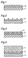
- the stripe-shaped or island-shaped concave-convex structure may be formed so as to leave semiconductor layer 12 as shown in Fig.2.
- the concave-convex structure may be formed so as to penetrate the nitride layer 12 and remove a part of the auxiliary substrate 11. Forming concave-convex structure in such a depth as removing the part of the auxiliary substrate 11, a distortion of crystal is suppressed at a point that the single-crystal GaN laterally grown from the convex part meets with each other. This improves the crystallinity of the single-crystal GaN.
- the nitride semiconductor 12 may has a two-layer structure of GaN-on-AIGaN, in which concave-convex structure is formed in such a depth that a part of the AIGaN is removed. Next, as shown in Fig.
- a single-crystal GaN 13 is grown over the concave-convex structure of the nitride semiconductor layer 12. In this manner, a GaN substrate comprising nitride semiconductor layers and an auxiliary substrate is obtained. If a GaN substrate made only of nitride semiconductor is required, the single-crystal GaN layer is grown thick by, for example, a HVPE method and, then, the auxiliary substrate 11 such as a sapphire substrate is removed.
- the thickness of the nitride semiconductor part of the GaN substrate is preferably not more than 100 ⁇ m, more preferably not more than 50 ⁇ m and most preferably, not more than 20 ⁇ m.
- the lower limit of the thickness may be any value as long as the protective film or the unevenness is covered by ELOG grown GaN to decrease dislocations.
- the lower limit of the thickness is not less than several ⁇ m.
- the thickness of the GaN substrate made only of nitride semiconductor is not limited to a specific value in the present invention. But the thickness is preferably in a range of 50 to 500 ⁇ m and more preferably, in a range of 100 to 300 ⁇ m. When the thickness of the GaN substrate is within the above-mentioned range, the dislocations can be decreased and the mechanical strength can be held.
- a mask made of, for example, SiO 2 is formed on the single-crystal GaN layer 13 in a stripe-like or island-like shape periodically, and a single-crystal GaN layer is laterally grown over the mask by the CVD method (Second growth of single-crystal GaN).
- the removal procedure is preferably done after the first growth of the single-crystal GaN 13. It is preferable that the surface of the firstly grown single-crystal GaN 13 is made smooth by etching before the second growth of the single-crystal GaN.
- the single-crystal GaN With the first growth of the single-crystal GaN in which the concave-convex structure is made and the GaN is grown by the HVPE method, a thick single-crystal GaN layer is easily obtained. However, this single-crystal GaN layer is apt to have voids near the concave structure and have an insufficient crystallinity.
- the second growth of the single-crystal GaN layer by the MOCVD method using the SiO 2 mask provides a single-crystal GaN layer having better crystallinity.
- the GaN substrate tends to be warped a little. This indicates that the surface of the GaN layer from which the auxiliary substrate is removed is different in physical properties from the grown surface of the GaN layer.
- the problem of occurring small cracks may be caused by the difference in physical properties of the surfaces. In any case, growing a layer having a small coefficient of thermal expansion, for example Al a Ga 1- a N, on a GaN substrate, small cracks are prevented and semiconductor device having good crystalinity is obtained.
- the small cracks are prevented by the compressive strain laid on the device-forming layer contacting the GaN substrate.
- the device is preferably a light-emitting device comprising a n-type cladding layer containing Al, an active layer containing InGaN and a p-type cladding layer containing Al. Taking this device structure, with the effect of the prevention of crack forming, a good characteristics device is obtained.
- every method to grow nitride semiconductors which is known, such as MOVPE(metal-organic vapor-phase epitaxy), MOCVD(metal-organic chemical vapor deposition), HVPE(halide vapor-phase epitaxy), MBE(molecular beam epitaxy) and the like, can be used.
- MOVPE metal-organic vapor-phase epitaxy
- MOCVD metal-organic chemical vapor deposition
- HVPE halide vapor-phase epitaxy
- MBE molecular beam epitaxy
- Example 1 the nitride semiconductor laser device as shown in Fig. 5 was manufactured.
- the GaN substrate was manufactured according to each step as shown in Figs. 1 to 4.
- a sapphire substrate 11 of two-inch in diameter having its principal surface represented by a C-face and an orientation flat face represented by an A-face was set in the reactor and the temperature was adjusted to 510 °C.
- a buffer layer (not shown) made of GaN which has a thickness of about 200 angstroms was grown using hydrogen as a carrier gas and ammonia and TMG (trimethylgallium) as a source of GaN on the sapphire substrate.
- a first nitride semiconductor layer 12 made of undoped GaN was grown to the thickness of 2 ⁇ m (Fig.1).
- a photo-mask having stripes was formed.
- the SiO 2 film which was patterned to have a stripe width (the upper part of the convex portion) of 5 ⁇ m and a stripe distance (the bottom part of the concave portion) of 15 ⁇ m was formed with a sputtering apparatus.
- the first nitride semiconductor layer 12 on which the SiO 2 film was not formed was etched with a RIE apparatus to the extent that the nitride semiconductor 12 remained, so as to form a concave-convex structure.
- the first nitride semiconductor 12 was exposed on the side face of the concave portion (Fig.2).
- SiO 2 was removed from the upper part of the convex portion.
- the stripe was formed in the direction perpendicular to the orientation flat face.
- a second nitride semiconductor layer 13 made of undoped GaN was grown to the thickness of about 320 ⁇ m using TMG and ammonia as a source of GaN (Fig.3 and Fig.4).
- the wafer was removed out of the reactor, so as to obtain a GaN substrate 30 made of undoped GaN.
- the sapphire substrate was removed from the resulting GaN substrate 30 and the device structure as described below was grown on the growth surface opposite to the removal surface, as shown in Flg.5.
- the thickness of the substrate made of GaN was about 300 ⁇ m.
- An undoped n-type contact layer 1 made of undoped Al 0.05 Ga 0.95 N was grown to the thickness of 1 ⁇ m on the GaN substrate 30, using TMA (trimethylalminium), TMG and ammonia gas as a source gas at 1050 °C.
- n-type contact layer 2 Al a Ga 1-a N of the present invention
- an n-type contact layer 2 made of Al 0.05 Ga 0.95 N doped with Si to 3 ⁇ 10 18 /cm 3 was grown to the thickness of 3 ⁇ m, using TMA, TMG and ammonia gas as a source gas and a silane gas (SIH 4 ) as an impurity gas.
- the cracks can be prevented well. If there are any small cracks in tha GaN substrate, the small cracks can be prevented from propagating by growing the n-type nitride semiconductor layer 2, so as to grow a device structure having a good crystallinity. The crystallinity was enhanced better in the case that both an n-type contact layer 2 and an undoped n-type contact layer 1 are formed as described above, compared with the case that only the n-type contact layer 2 was formed.
- a crack preventing layer 3 made of In 0.08 Ga 0.92 N doped with Si to 5 ⁇ 10 18 /cm 3 was grown to the thickness of 0.15 ⁇ m, using TMG, TMI (trimethylindium) and ammonia gas as a source gas and a silane gas as an impurity gas.
- a layer made of undoped Al 0.14 Ga 0.86 N was grown to the thickness of 25 angstroms using TMA, TMG and ammonia as a source gas.
- TMA was stopped and B layer made of GaN doped with Si to 5 ⁇ 10 18 /cm 3 was grown to the thickness of 25 angstroms, using a silane gas as an impurity gas.
- an n-type waveguide layer made of undoped GaN was grown to the thickness of 0.075 ⁇ m using TMG and ammonia as a source gas.
- a barrier layer made of In 0.01 Ga 0.99 N doped with Si to 5 ⁇ 10 18 /cm 3 was grown to the thickness of 100 angstroms using TMI, TMG and ammonia as a source gas and silane gas as an impurity gas. Subsequently, the silane gas was stopped and an well layer made. of undoped In 0.11 Ga 0.89 N was grown to the thickness of 50 angstroms. The operation was three times and finally, a barrier layer was laminated, with the result that the active layer 6 in the multiple quantum well structure (MQW) having a total thickness of 550 angstroms was obtained.
- MQW multiple quantum well structure
- a p-type electron confining layer 7 made of Al 0.4 Ga 0.6 N doped with Mg to 1 ⁇ 10 19 /cm 3 was grown to the thickness of 100 angstroms using TMA, TMG and ammonia as a source gas and Cp 2 Mg (cyclopentadienylmagnesium) as an impurity gas.
- a p-type waveguide layer 8 made of undoped GaN was grown to the thickness of 0.075 ⁇ m using TMG and ammonia as a source gas.
- This p-type guide layer 8 was an undoped one but due to the diffusion of Mg from the p-type electron confining layer 7, the concentration of Mg was 5 ⁇ 10 16 /cm 3 , resulting in showing a p-type conductivity.
- a layer made of undoped Al 0.1 Ga 0.9 N was grown to the thickness of 25 angstroms using TMA, TMG and ammonia as a source gas.
- TMA was stopped and B layer made of GaN doped with Mg to 5 ⁇ 10 18 /cm 3 was grown to the thickness of 25 angstroms, using Cp 2 Mg gas as an impurity gas.
- Cp 2 Mg gas as an impurity gas.
- a p-type contact layer 10 made of GaN doped with Mg to 1 ⁇ 10 20 /cm 3 was grown to the thickness of 150 angstroms, using TMG and ammonia as a source gas and Cp 2 Mg gas as an impurity gas.
- the wafer was annealed at 700°C in nitrogen atmosphere within the reactor, so as to make the p-type layers less resistive.
- etching was conducted by SiCl 4 with RIE (reactive ion etching) apparatus, to expose the surface of the n-side contact layer 2 on which an n-electrode was to be formed, as shown in Fig. 5.
- a first protective film 61 made of Si oxide (mainly, SiO 2 ) was formed to the thickness of 0.5 ⁇ m on the almost entire surface of the uppermost p-side contact layer 10 with PVD apparatus. Thereafter, a mask of a predetermined shape was placed on the first protective film 61 and a third protective film 63 made of photo resist having a stripe width of 1.8 ⁇ m and a thickness of 1 ⁇ m was formed.
- the p-side contact layer 10 and the p-side cladding layer 9 were again etched using SiCl 4 gas with the RIE to form a ridge stripe having a stripe width of 1.8 ⁇ m.
- a second protective film 62 made of Zr oxide (mainly ZrO 2 ) was formed to the thickness of 0.5 ⁇ m continuously on the first protective film 61 and on the p-side cladding layer 9 which had been exposed by etching.
- Zr oxide was formed in this way, the insulation of p-n surface can be established and the transverse mode can be stabilized.
- the wafer was soaked in hydrofluoric acid and as shown in Fig. 6F, the first protective film 61 was removed using a lift-off method.
- a p-electrode 20 made of Ni/Au was formed on the surface of the p-side contact layer 10 which was exposed by removing the first protective film 61 on said p-side contact layer.
- the p-electrode 20 had a stripe width of 100 ⁇ m and was formed in a manner to extend over the second protective film, as shown in this drawing.
- an n-electrode 21 made of Ti/Al was formed parallel to the stripe on the exposed n-side contact layer.
- the resulting laser device was set on the heat sink and each electrode was connected by wire-bonding.
- the laser oscillation was tried at room temperature.
- the continuous oscillation at a wavelength of 500 nm was observed at the threshold current density of 2.5 kA/cm 2 and the threshold voltage of 5V at room temperature.
- the lifetime was ten thousand hours or longer at room temperature.
- the laser device was fabricated in the same manner as in Example 1, except that the undoped n-type contact layer 1 was not grown and only the n-type contact layer 2 was grown.
- the resulting device had a crystallinity which was a little worse than that in Example 1. But small cracks could be prevented almost like in Example 1 and good device characteristics could be achieved.
- the laser device was fabricated in the same manner as in Example 1, except that the ratio of Al in the undoped n-type contact layer 1 and the Si-doped n-type contact layer 2 was changed from 0.05 to 0.2.
- the resulting device showed good result almost like in Example 1.
- the laser device was fabricated in the same manner as in Example 1, except that the ratio of Al in the undoped n-type contact layer 1 and the Si-doped n-type contact layer 2 was changed from 0.05 to 0.5.
- the resulting device had a crystallinity which was a little worse than that in Example 1 because the ratio of Al was larger than in Example 1. But small cracks could be prevented almost like in Example 1 and good device characteristics could be achieved.
- the laser device was fabricated in the same manner as in Example 1, except that the undoped n-type contact layer 1 and the Si-doped n-type contact layer 2 were made of AIN.
- the resulting device had a crystallinity which was a little worse than that in Example 1 because the ratio of Al in the n-type contact layer 1 and the n-type contact layer was larger than in Example 1. But small cracks could be prevented almost like in Example 1 and as long a lifetime as in Example 1 could be achieved.
- the laser device was fabricated in the same manner as in Example 1, except that the second nitride semiconductor 13 had a thickness of 15 ⁇ m and the sapphire substrate was not removed.
- the obtained GaN substrate comprised the auxiliary substrate and the nitride semiconductor.
- the resulting laser device tended to have a little large warp, compared with in Example 1, but small cracks could be prevented like in Example 1. Since the laser device of Example 6 had an isolating sapphire substrate, the heat radiation property of the device was a little bad, compared with in Example 1. But as long a lifetime as in Example 1 could be achieved.
Landscapes
- Chemical & Material Sciences (AREA)
- Physics & Mathematics (AREA)
- Crystallography & Structural Chemistry (AREA)
- Condensed Matter Physics & Semiconductors (AREA)
- Optics & Photonics (AREA)
- Materials Engineering (AREA)
- Metallurgy (AREA)
- Organic Chemistry (AREA)
- Electromagnetism (AREA)
- Engineering & Computer Science (AREA)
- General Physics & Mathematics (AREA)
- Chemical Kinetics & Catalysis (AREA)
- General Chemical & Material Sciences (AREA)
- Inorganic Chemistry (AREA)
- Semiconductor Lasers (AREA)
- Led Devices (AREA)
- Recrystallisation Techniques (AREA)
- Formation Of Insulating Films (AREA)
Abstract
Description
Claims (8)
- A nitride semiconductor device comprising a GaN substrate having a single-crystal GaN layer at least on its surface and plurality of device-forming layers made of nitride semiconductor and formed on said GaN substrate,
wherein a compressive strain is applied to said device-forming layer which is contacting said GaN substrate. - The nitride semiconductor device according to claim 1, wherein said device-forming layer contacting said GaN substrate has a coefficient of thermal expansion smaller than that of GaN.
- The nitride semiconductor device according to claim 1, wherein said device-forming layer contacting said GaN substrate is made of AlaGa1-aN, (0< a ≦ 1).
- The nitride semiconductor device according to claim 3, wherein said device-forming layers include an n-type cladding layer containing Al, an active layer containing InGaN and a p-type cladding layer containing Al.
- The nitride semiconductor device according to claim 4, wherein said device-forming layer made of AlaGa1-aN functions as an n-type contact layer.
- The nitride semiconductor device according to claim 1, wherein said single-crystal GaN layer is formed through lateral-growth process.
- A method of manufacturing a nitride semiconductor device, which includes a GaN substrate having a single-crystal GaN layer at least on its surface and plurality of device-forming layers made of nitride semiconductor formed on said GaN layer, comprising the steps of;forming a first nitride semiconductor layer on a auxiliary substrate made of different material from nitride semiconductor;forming a stripe-shaped or island-shaped periodical concave-convex structure on said first nitride semiconductor layer;forming a single-crystal GaN layer to make a GaN substrate; andforming a second nitride semiconductor layer on said GaN substrate, the second nitride semiconductor layer having a coefficient of thermal expansion smaller than that of GaN.
- The method of manufacturing a nitride semiconductor device acording to claim 7, wherein said auxiliary substrate is removed after forming said single-crystal GaN layer to make GaN substrate.
Applications Claiming Priority (5)
| Application Number | Priority Date | Filing Date | Title |
|---|---|---|---|
| JP3099099 | 1999-02-09 | ||
| JP3099099 | 1999-02-09 | ||
| JP33179799A JP3770014B2 (en) | 1999-02-09 | 1999-11-22 | Nitride semiconductor device |
| JP33179799 | 1999-11-22 | ||
| PCT/JP2000/000660 WO2000048254A1 (en) | 1999-02-09 | 2000-02-08 | Nitride semiconductor device and its manufacturino method |
Publications (3)
| Publication Number | Publication Date |
|---|---|
| EP1184913A1 true EP1184913A1 (en) | 2002-03-06 |
| EP1184913A4 EP1184913A4 (en) | 2007-07-04 |
| EP1184913B1 EP1184913B1 (en) | 2018-10-10 |
Family
ID=26369449
Family Applications (1)
| Application Number | Title | Priority Date | Filing Date |
|---|---|---|---|
| EP00902126.2A Expired - Lifetime EP1184913B1 (en) | 1999-02-09 | 2000-02-08 | Nitride semiconductor laser diode |
Country Status (8)
| Country | Link |
|---|---|
| US (2) | US6835956B1 (en) |
| EP (1) | EP1184913B1 (en) |
| JP (1) | JP3770014B2 (en) |
| KR (1) | KR100634340B1 (en) |
| CN (1) | CN1157804C (en) |
| AU (1) | AU771942B2 (en) |
| TW (1) | TW443018B (en) |
| WO (1) | WO2000048254A1 (en) |
Cited By (1)
| Publication number | Priority date | Publication date | Assignee | Title |
|---|---|---|---|---|
| US7177336B2 (en) | 2002-04-04 | 2007-02-13 | Sharp Kabushiki Kaisha | Semiconductor laser device |
Families Citing this family (40)
| Publication number | Priority date | Publication date | Assignee | Title |
|---|---|---|---|---|
| JP3587081B2 (en) | 1999-05-10 | 2004-11-10 | 豊田合成株式会社 | Method of manufacturing group III nitride semiconductor and group III nitride semiconductor light emitting device |
| JP3555500B2 (en) | 1999-05-21 | 2004-08-18 | 豊田合成株式会社 | Group III nitride semiconductor and method of manufacturing the same |
| US6580098B1 (en) | 1999-07-27 | 2003-06-17 | Toyoda Gosei Co., Ltd. | Method for manufacturing gallium nitride compound semiconductor |
| JP3427047B2 (en) * | 1999-09-24 | 2003-07-14 | 三洋電機株式会社 | Nitride-based semiconductor device, method of forming nitride-based semiconductor, and method of manufacturing nitride-based semiconductor device |
| JP2001185493A (en) * | 1999-12-24 | 2001-07-06 | Toyoda Gosei Co Ltd | Method of manufacturing group III nitride compound semiconductor and group III nitride compound semiconductor device |
| JP4432180B2 (en) | 1999-12-24 | 2010-03-17 | 豊田合成株式会社 | Group III nitride compound semiconductor manufacturing method, group III nitride compound semiconductor device, and group III nitride compound semiconductor |
| JP2001267242A (en) | 2000-03-14 | 2001-09-28 | Toyoda Gosei Co Ltd | Group III nitride compound semiconductor and method of manufacturing the same |
| EP1265273A4 (en) | 2000-03-14 | 2009-05-06 | Toyoda Gosei Kk | PROCESS FOR PRODUCING NITRIDE III COMPOUND SEMICONDUCTOR AND SEMICONDUCTOR COMPONENT BASED ON NITRIDE III COMPOUND |
| TW518767B (en) | 2000-03-31 | 2003-01-21 | Toyoda Gosei Kk | Production method of III nitride compound semiconductor and III nitride compound semiconductor element |
| JP2001313259A (en) | 2000-04-28 | 2001-11-09 | Toyoda Gosei Co Ltd | Method for manufacturing group III nitride compound semiconductor substrate and semiconductor device |
| AU2001279163A1 (en) * | 2000-08-04 | 2002-02-18 | The Regents Of The University Of California | Method of controlling stress in gallium nitride films deposited on substrates |
| US7619261B2 (en) | 2000-08-07 | 2009-11-17 | Toyoda Gosei Co., Ltd. | Method for manufacturing gallium nitride compound semiconductor |
| JP2002222746A (en) * | 2001-01-23 | 2002-08-09 | Matsushita Electric Ind Co Ltd | Nitride semiconductor wafer and method for manufacturing the same |
| EP1367150B1 (en) | 2001-02-14 | 2009-08-19 | Toyoda Gosei Co., Ltd. | Production method for semiconductor crystal and semiconductor luminous element |
| JP3679720B2 (en) | 2001-02-27 | 2005-08-03 | 三洋電機株式会社 | Nitride semiconductor device and method for forming nitride semiconductor |
| JP2002280314A (en) | 2001-03-22 | 2002-09-27 | Toyoda Gosei Co Ltd | Method of manufacturing group III nitride compound semiconductor and group III nitride compound semiconductor device based thereon |
| JP3690326B2 (en) | 2001-10-12 | 2005-08-31 | 豊田合成株式会社 | Method for producing group III nitride compound semiconductor |
| KR100427689B1 (en) * | 2002-02-21 | 2004-04-28 | 엘지전자 주식회사 | Method for manufacturing Nitride semiconductor substrate |
| US7485902B2 (en) * | 2002-09-18 | 2009-02-03 | Sanyo Electric Co., Ltd. | Nitride-based semiconductor light-emitting device |
| US7078743B2 (en) * | 2003-05-15 | 2006-07-18 | Matsushita Electric Industrial Co., Ltd. | Field effect transistor semiconductor device |
| JP4218597B2 (en) * | 2003-08-08 | 2009-02-04 | 住友電気工業株式会社 | Manufacturing method of semiconductor light emitting device |
| JP4011569B2 (en) | 2003-08-20 | 2007-11-21 | 株式会社東芝 | Semiconductor light emitting device |
| JP4540347B2 (en) | 2004-01-05 | 2010-09-08 | シャープ株式会社 | Nitride semiconductor laser device and manufacturing method thereof |
| JP4201725B2 (en) | 2004-02-20 | 2008-12-24 | シャープ株式会社 | Manufacturing method of nitride semiconductor light emitting device |
| JP2005294753A (en) * | 2004-04-05 | 2005-10-20 | Toshiba Corp | Semiconductor light emitting device |
| US7157297B2 (en) | 2004-05-10 | 2007-01-02 | Sharp Kabushiki Kaisha | Method for fabrication of semiconductor device |
| JP4651312B2 (en) | 2004-06-10 | 2011-03-16 | シャープ株式会社 | Manufacturing method of semiconductor device |
| JP4371029B2 (en) * | 2004-09-29 | 2009-11-25 | サンケン電気株式会社 | Semiconductor light emitting device and manufacturing method thereof |
| JP5155536B2 (en) * | 2006-07-28 | 2013-03-06 | 一般財団法人電力中央研究所 | Method for improving the quality of SiC crystal and method for manufacturing SiC semiconductor device |
| TWI341600B (en) * | 2007-08-31 | 2011-05-01 | Huga Optotech Inc | Light optoelectronic device and forming method thereof |
| JP2009190936A (en) * | 2008-02-14 | 2009-08-27 | Sumitomo Electric Ind Ltd | Method for producing group III nitride crystal |
| US20100200880A1 (en) * | 2008-06-06 | 2010-08-12 | Hong Kong Applied Science And Technology Research Institute Co. Ltd. | Semiconductor wafers and semiconductor devices and methods of making semiconductor wafers and devices |
| US8395168B2 (en) * | 2008-06-06 | 2013-03-12 | Hong Kong Applied Science And Technology Research Institute Co. Ltd. | Semiconductor wafers and semiconductor devices with polishing stops and method of making the same |
| JP5591800B2 (en) | 2008-06-30 | 2014-09-17 | ユニバーサル・ディスプレイ・コーポレーション | Hole transport material containing triphenylene |
| JP5536054B2 (en) | 2008-06-30 | 2014-07-02 | ユニバーサル・ディスプレイ・コーポレーション | Hole transport material having sulfur-containing groups |
| DE102011077542B4 (en) * | 2011-06-15 | 2020-06-18 | Osram Opto Semiconductors Gmbh | OPTOELECTRONIC SEMICONDUCTOR BODY AND METHOD FOR PRODUCING AN OPTOELECTRONIC SEMICONDUCTOR BODY |
| KR102369933B1 (en) * | 2015-08-03 | 2022-03-04 | 삼성전자주식회사 | Semiconductor light emitting device and method for manufacturing the same |
| DE102016125430A1 (en) * | 2016-12-22 | 2018-06-28 | Osram Opto Semiconductors Gmbh | Surface-mountable semiconductor laser, arrangement with such a semiconductor laser and operating method therefor |
| PL3767762T3 (en) | 2019-07-14 | 2022-12-12 | Instytut Wysokich Ciśnień Polskiej Akademii Nauk | Distributed feedback laser diode and method of making the same |
| CN110783176B (en) * | 2019-10-30 | 2022-07-12 | 广西大学 | Preparation method of low-stress semiconductor material |
Family Cites Families (352)
| Publication number | Priority date | Publication date | Assignee | Title |
|---|---|---|---|---|
| NL6405927A (en) | 1963-06-07 | 1964-12-08 | ||
| DE1614574A1 (en) | 1967-08-04 | 1970-10-29 | Siemens Ag | Semiconductor component, in particular a semiconductor component with a pn junction |
| FR1597033A (en) | 1968-06-19 | 1970-06-22 | ||
| DE1789061A1 (en) | 1968-09-30 | 1971-12-23 | Siemens Ag | Laser diode |
| DE1913676A1 (en) | 1969-03-18 | 1970-09-24 | Siemens Ag | Method for depositing layers of semiconducting or insulating material from a flowing reaction gas on heated semiconductor crystals or for doping such crystals from a flowing doping gas |
| US4020791A (en) | 1969-06-30 | 1977-05-03 | Siemens Aktiengesellschaft | Apparatus for indiffusing dopants into semiconductor material |
| US4404265A (en) | 1969-10-01 | 1983-09-13 | Rockwell International Corporation | Epitaxial composite and method of making |
| US3853974A (en) | 1970-04-06 | 1974-12-10 | Siemens Ag | Method of producing a hollow body of semiconductor material |
| DE2033444C3 (en) | 1970-07-06 | 1979-02-15 | Siemens Ag | Device for diffusing dopants into wafers made of semiconductor material |
| US3737737A (en) | 1970-10-09 | 1973-06-05 | Siemens Ag | Semiconductor diode for an injection laser |
| DE2125085C3 (en) | 1971-05-19 | 1979-02-22 | Siemens Ag, 1000 Berlin Und 8000 Muenchen | Device for manufacturing tubes closed on one side from semiconductor material |
| DE2158257A1 (en) | 1971-11-24 | 1973-05-30 | Siemens Ag | ARRANGEMENT FOR THE MANUFACTURING OF SINGLE-SIDED TUBES FROM SEMICONDUCTOR MATERIAL |
| US3941647A (en) | 1973-03-08 | 1976-03-02 | Siemens Aktiengesellschaft | Method of producing epitaxially semiconductor layers |
| US3819974A (en) | 1973-03-12 | 1974-06-25 | D Stevenson | Gallium nitride metal-semiconductor junction light emitting diode |
| DE2346198A1 (en) | 1973-07-27 | 1975-05-07 | Siemens Ag | METHOD FOR MANUFACTURING YELLOW LUMINOUS GALLIUMPHOSPHIDE DIODES |
| DE2340225A1 (en) | 1973-08-08 | 1975-02-20 | Siemens Ag | METHOD FOR MANUFACTURING DIRECT HEATABLE HOLLOW BODIES FROM SEMICONDUCTOR MATERIAL |
| IE39673B1 (en) | 1973-10-02 | 1978-12-06 | Siemens Ag | Improvements in or relating to semiconductor luminescence diodes |
| FR2251104B1 (en) | 1973-11-14 | 1978-08-18 | Siemens Ag | |
| US4062035A (en) | 1975-02-05 | 1977-12-06 | Siemens Aktiengesellschaft | Luminescent diode |
| DE2528192C3 (en) | 1975-06-24 | 1979-02-01 | Siemens Ag, 1000 Berlin Und 8000 Muenchen | Device for depositing elemental silicon on a rod-shaped support body made of elemental silicon |
| US4098223A (en) | 1976-05-03 | 1978-07-04 | Siemens Aktiengesellschaft | Apparatus for heat treating semiconductor wafers |
| DE2644208C3 (en) | 1976-09-30 | 1981-04-30 | Siemens AG, 1000 Berlin und 8000 München | Process for the production of a monocrystalline layer on a substrate |
| DE2643893C3 (en) | 1976-09-29 | 1981-01-08 | Siemens Ag, 1000 Berlin Und 8000 Muenchen | Process for the production of a layer provided with a structure on a substrate |
| US4108539A (en) | 1976-11-18 | 1978-08-22 | Hewlett-Packard Company | Reflecting lens system |
| US4113381A (en) | 1976-11-18 | 1978-09-12 | Hewlett-Packard Company | Surveying instrument and method |
| DE2716143A1 (en) | 1977-04-12 | 1978-10-19 | Siemens Ag | LIGHT-EMITTING SEMI-CONDUCTOR COMPONENT |
| US4154625A (en) | 1977-11-16 | 1979-05-15 | Bell Telephone Laboratories, Incorporated | Annealing of uncapped compound semiconductor materials by pulsed energy deposition |
| DE2910723A1 (en) | 1979-03-19 | 1980-09-25 | Siemens Ag | METHOD FOR PRODUCING EPITACTIC SEMICONDUCTOR MATERIAL LAYERS ON SINGLE CRYSTALLINE SUBSTRATES AFTER THE LIQUID PHASE SHIFT EPITAXY |
| DE3003285A1 (en) | 1980-01-30 | 1981-08-06 | Siemens AG, 1000 Berlin und 8000 München | METHOD FOR PRODUCING LOW-RESISTANT, SINGLE-CRYSTAL METAL OR ALLOY LAYERS ON SUBSTRATES |
| DE3016778A1 (en) | 1980-04-30 | 1981-11-05 | Siemens AG, 1000 Berlin und 8000 München | LASER DIODE |
| US4423349A (en) | 1980-07-16 | 1983-12-27 | Nichia Denshi Kagaku Co., Ltd. | Green fluorescence-emitting material and a fluorescent lamp provided therewith |
| DE3208638A1 (en) | 1982-03-10 | 1983-09-22 | Siemens AG, 1000 Berlin und 8000 München | SILICON CARBIDE LUMINESCENCE DIODE |
| JPS58158972A (en) | 1982-03-16 | 1983-09-21 | Toshiba Corp | Manufacture of semiconductor device |
| DE3210086A1 (en) | 1982-03-19 | 1983-09-22 | Siemens AG, 1000 Berlin und 8000 München | LUMINESCENCE DIODE, SUITABLE AS PRESSURE SENSOR |
| DE3227263C2 (en) | 1982-07-21 | 1984-05-30 | Siemens AG, 1000 Berlin und 8000 München | Method of manufacturing a planar avalanche photodiode with a long-wave sensitivity limit above 1.3 µm. |
| US4568206A (en) | 1983-04-25 | 1986-02-04 | Nichia Seimitsu Kogyo Co., Ltd. | Retainer for ball bearing |
| DE3328902A1 (en) | 1983-08-10 | 1985-02-28 | Siemens AG, 1000 Berlin und 8000 München | DISPLAY WITH A NUMBER OF LIGHT-EMITTING SEMICONDUCTOR COMPONENTS |
| DE3338335A1 (en) | 1983-10-21 | 1985-05-09 | Siemens AG, 1000 Berlin und 8000 München | METHOD FOR PRODUCING LARGE-SIDED SILICON CRYSTAL BODIES FOR SOLAR CELLS |
| DE3413667A1 (en) | 1984-04-11 | 1985-10-17 | Siemens AG, 1000 Berlin und 8000 München | METHOD FOR ADJUSTING A COUPLING OPTICS PROVIDED AT THE END OF AN OPTICAL WAVE GUIDE TO A SEMICONDUCTOR LASER, AND DEVICE FOR CARRYING OUT THE METHOD |
| DE3421215A1 (en) | 1984-06-07 | 1985-12-12 | Aeg-Telefunken Ag, 1000 Berlin Und 6000 Frankfurt | METHOD FOR PRODUCING INGAASP AND INGAAS - DOUBLE HETEROSTRUCTURAL LASERS AND LED'S BY MEANS OF LIQUID PHASE EPITAXY FOR A WAVELENGTH RANGE FROM (LAMBDA) = 1.2 (MY) M TO 1.7 (MY) M |
| US4599244A (en) | 1984-07-11 | 1986-07-08 | Siemens Aktiengesellschaft | Method large-area silicon bodies |
| US4722088A (en) | 1984-09-14 | 1988-01-26 | Siemens Aktiengesellschaft | Semiconductor laser for high optical output power with reduced mirror heating |
| DE3434741A1 (en) | 1984-09-21 | 1986-04-03 | Siemens AG, 1000 Berlin und 8000 München | COUPLED LASER DIODE ARRANGEMENT |
| DE3435148A1 (en) | 1984-09-25 | 1986-04-03 | Siemens AG, 1000 Berlin und 8000 München | LASER DIODE WITH BURNED ACTIVE LAYER AND WITH LATERAL CURRENT LIMITATION BY SELF-ADJUSTED PN TRANSITION AND METHOD FOR PRODUCING SUCH A LASER DIODE |
| US4683574A (en) | 1984-09-26 | 1987-07-28 | Siemens Aktiengesellschaft | Semiconductor laser diode with buried hetero-structure |
| EP0178497B1 (en) | 1984-10-03 | 1990-11-28 | Siemens Aktiengesellschaft | Method for producing in an integrated form a dfb laser coupled with a strip waveguide on a substrate |
| US4615766A (en) | 1985-02-27 | 1986-10-07 | International Business Machines Corporation | Silicon cap for annealing gallium arsenide |
| DE3610333A1 (en) | 1985-04-19 | 1986-11-27 | Siemens AG, 1000 Berlin und 8000 München | Method for producing a surface grating (lattice, grid) having a specific grating constant on a lower-lying surface region of a mesastructure |
| JPS62246988A (en) | 1986-04-18 | 1987-10-28 | Nichia Chem Ind Ltd | X-ray phosphor and x-ray sensitized paper |
| US5250366A (en) | 1985-05-18 | 1993-10-05 | Nichia Kagaku Kogyo K.K. | Phosphor which emits light by the excitation of X-ray, and a X-ray intensifying screen using the phosphor |
| US4959174A (en) | 1985-05-18 | 1990-09-25 | Nichia Kagaku Kogyo K.K. | Phosphor which emits light by the excitation of X-ray |
| DE3531734A1 (en) | 1985-09-05 | 1987-03-12 | Siemens Ag | DEVICE FOR POSITIONING A SEMICONDUCTOR LASER WITH SELF-ADJUSTING EFFECT FOR A FIBER TO BE COUPLED |
| DE3532821A1 (en) | 1985-09-13 | 1987-03-26 | Siemens Ag | LIGHT-EMITTING DIODE (LED) WITH SPHERICAL LENS |
| DE3534017A1 (en) | 1985-09-24 | 1987-03-26 | Siemens Ag | METHOD FOR COUPLING A LASER DIODE TO A MONOMODE LIGHT WAVE GUIDE, AND AN ARRANGEMENT OF A LASER DIODE AND A LIGHT WAVE GUIDE COUPLED TO IT |
| EP0236713A3 (en) | 1986-02-10 | 1988-06-29 | Siemens Aktiengesellschaft | Laser diode |
| EP0237812A3 (en) | 1986-03-20 | 1988-06-29 | Siemens Aktiengesellschaft | Semiconductor laser array with a collimated beam |
| DE3611167A1 (en) | 1986-04-03 | 1987-10-08 | Siemens Ag | ARRAY WITH COUPLED OPTICAL WAVE GUIDES |
| US4818722A (en) | 1986-09-29 | 1989-04-04 | Siemens Aktiengesellschaft | Method for generating a strip waveguide |
| JPH0662943B2 (en) | 1986-10-06 | 1994-08-17 | 日亜化学工業株式会社 | Fluorescent material for radiographic intensifying screen |
| US4911102A (en) | 1987-01-31 | 1990-03-27 | Toyoda Gosei Co., Ltd. | Process of vapor growth of gallium nitride and its apparatus |
| US5218216A (en) | 1987-01-31 | 1993-06-08 | Toyoda Gosei Co., Ltd. | Gallium nitride group semiconductor and light emitting diode comprising it and the process of producing the same |
| JPS63224252A (en) | 1987-02-06 | 1988-09-19 | シーメンス、アクチエンゲゼルシヤフト | Waveguide-photodiode array |
| DE3870651D1 (en) | 1987-02-20 | 1992-06-11 | Siemens Ag | LASER TRANSMITTER ARRANGEMENT. |
| JPH0630242B2 (en) | 1987-03-04 | 1994-04-20 | 陽一 峰松 | Ultraviolet fluorescent lamps for artificial accelerated exposure testing of polymeric materials |
| DE3810245A1 (en) | 1987-03-27 | 1988-10-06 | Japan Incubator Inc | LIGHT-EMITTING ELEMENT AND METHOD FOR THE PRODUCTION THEREOF |
| DE3711617A1 (en) | 1987-04-07 | 1988-10-27 | Siemens Ag | MONOLITHICALLY INTEGRATED WAVE GUIDE-PHOTODIODE-FET COMBINATION |
| US4855118A (en) | 1987-04-15 | 1989-08-08 | Nichia Kagaku Kogyo K.K. | Method of producing fluorapatite |
| US5011550A (en) * | 1987-05-13 | 1991-04-30 | Sharp Kabushiki Kaisha | Laminated structure of compound semiconductors |
| JPH0774333B2 (en) | 1987-06-29 | 1995-08-09 | 日亜化学工業株式会社 | Luminescent composition |
| DE3727546A1 (en) | 1987-08-18 | 1989-03-02 | Siemens Ag | LIGHT AMPLIFIER WITH RING-SHAPED RADIATION, IN PARTICULAR RING LASER DIODE |
| DE3731312C2 (en) | 1987-09-17 | 1997-02-13 | Siemens Ag | Process for separating monolithically manufactured laser diodes |
| EP0309744A3 (en) | 1987-09-29 | 1989-06-28 | Siemens Aktiengesellschaft | Arrangement with a thin-film waveguide extending in a flat manner |
| US4960728A (en) | 1987-10-05 | 1990-10-02 | Texas Instruments Incorporated | Homogenization anneal of II-VI compounds |
| DE8713875U1 (en) | 1987-10-15 | 1988-02-18 | Siemens AG, 1000 Berlin und 8000 München | Optical transmitter component |
| US4945394A (en) | 1987-10-26 | 1990-07-31 | North Carolina State University | Bipolar junction transistor on silicon carbide |
| US4947218A (en) | 1987-11-03 | 1990-08-07 | North Carolina State University | P-N junction diodes in silicon carbide |
| GB2212658B (en) | 1987-11-13 | 1992-02-12 | Plessey Co Plc | Solid state light source |
| JP2663483B2 (en) | 1988-02-29 | 1997-10-15 | 勝 西川 | Method of forming resist pattern |
| EP0331778B1 (en) | 1988-03-09 | 1992-01-15 | Hewlett-Packard GmbH | Output amplifier |
| US4864369A (en) | 1988-07-05 | 1989-09-05 | Hewlett-Packard Company | P-side up double heterojunction AlGaAs light-emitting diode |
| US5252499A (en) | 1988-08-15 | 1993-10-12 | Rothschild G F Neumark | Wide band-gap semiconductors having low bipolar resistivity and method of formation |
| US4904618A (en) | 1988-08-22 | 1990-02-27 | Neumark Gertrude F | Process for doping crystals of wide band gap semiconductors |
| EP0356059B1 (en) | 1988-08-15 | 2000-01-26 | Gertrude F. Neumark | Process for doping crystals of wide band gap semiconductors |
| DE3836802A1 (en) | 1988-10-28 | 1990-05-03 | Siemens Ag | SEMICONDUCTOR LASER ARRANGEMENT FOR HIGH OUTPUT PERFORMANCE IN LATERAL BASIC MODE |
| US4990466A (en) | 1988-11-01 | 1991-02-05 | Siemens Corporate Research, Inc. | Method for fabricating index-guided semiconductor laser |
| DE3838016A1 (en) | 1988-11-09 | 1990-05-10 | Siemens Ag | SEMICONDUCTOR LASER IN THE GAA1INAS SYSTEM |
| US4987576A (en) | 1988-11-30 | 1991-01-22 | Siemens Aktiengesellschaft | Electrically tunable semiconductor laser with ridge waveguide |
| US4982314A (en) | 1988-12-09 | 1991-01-01 | Nichia Kagaku Kogyo K.K. | Power source circuit apparatus for electro-luminescence device |
| US4907534A (en) | 1988-12-09 | 1990-03-13 | Siemens Aktiengesellschaft | Gas distributor for OMVPE Growth |
| US4918497A (en) | 1988-12-14 | 1990-04-17 | Cree Research, Inc. | Blue light emitting diode formed in silicon carbide |
| US5061972A (en) | 1988-12-14 | 1991-10-29 | Cree Research, Inc. | Fast recovery high temperature rectifying diode formed in silicon carbide |
| US5027168A (en) | 1988-12-14 | 1991-06-25 | Cree Research, Inc. | Blue light emitting diode formed in silicon carbide |
| CA2008176A1 (en) | 1989-01-25 | 1990-07-25 | John W. Palmour | Silicon carbide schottky diode and method of making same |
| JP2704181B2 (en) | 1989-02-13 | 1998-01-26 | 日本電信電話株式会社 | Method for growing compound semiconductor single crystal thin film |
| JPH0636349B2 (en) | 1989-02-22 | 1994-05-11 | 日亜化学工業株式会社 | Fluorescent lamp with ultraviolet reflective layer |
| JP3026087B2 (en) | 1989-03-01 | 2000-03-27 | 豊田合成株式会社 | Gas phase growth method of gallium nitride based compound semiconductor |
| DE59009909D1 (en) | 1989-04-19 | 1996-01-11 | Siemens Ag | Device with a crucible in an effusion cell of a molecular beam epitaxy system. |
| US5160492A (en) | 1989-04-24 | 1992-11-03 | Hewlett-Packard Company | Buried isolation using ion implantation and subsequent epitaxial growth |
| JP2809691B2 (en) | 1989-04-28 | 1998-10-15 | 株式会社東芝 | Semiconductor laser |
| JP2809692B2 (en) | 1989-04-28 | 1998-10-15 | 株式会社東芝 | Semiconductor light emitting device and method of manufacturing the same |
| US5049779A (en) | 1989-05-02 | 1991-09-17 | Nichia Kagaku Kogyo K.K. | Phosphor composition used for fluorescent lamp and fluorescent lamp using the same |
| EP0405214A3 (en) | 1989-06-27 | 1991-06-05 | Siemens Aktiengesellschaft | Pin-fet combination with buried p-type layer |
| US4985742A (en) | 1989-07-07 | 1991-01-15 | University Of Colorado Foundation, Inc. | High temperature semiconductor devices having at least one gallium nitride layer |
| JPH0357288A (en) | 1989-07-17 | 1991-03-12 | Siemens Ag | Devices with semiconductor lasers and their usage |
| US5119540A (en) | 1990-07-24 | 1992-06-09 | Cree Research, Inc. | Apparatus for eliminating residual nitrogen contamination in epitaxial layers of silicon carbide and resulting product |
| JPH07116429B2 (en) | 1989-08-25 | 1995-12-13 | 日亜化学工業株式会社 | Pigmented phosphor |
| US4966862A (en) | 1989-08-28 | 1990-10-30 | Cree Research, Inc. | Method of production of light emitting diodes |
| US4946547A (en) | 1989-10-13 | 1990-08-07 | Cree Research, Inc. | Method of preparing silicon carbide surfaces for crystal growth |
| US5366834A (en) | 1989-11-15 | 1994-11-22 | Nichia Kagaku Kogyo K.K. | Method of manufacturing a cathode ray tube phosphor screen |
| US5019746A (en) | 1989-12-04 | 1991-05-28 | Hewlett-Packard Company | Prefabricated wire leadframe for optoelectronic devices |
| US5008735A (en) | 1989-12-07 | 1991-04-16 | General Instrument Corporation | Packaged diode for high temperature operation |
| US5077145A (en) | 1989-12-26 | 1991-12-31 | Nichia Kagaku Kogyo K.K. | Phosphor for x-ray intensifying screen and x-ray intensifying screen |
| US5278433A (en) | 1990-02-28 | 1994-01-11 | Toyoda Gosei Co., Ltd. | Light-emitting semiconductor device using gallium nitride group compound with double layer structures for the n-layer and/or the i-layer |
| CA2037198C (en) | 1990-02-28 | 1996-04-23 | Toyoda Gosei Co., Ltd. | Light-emitting semiconductor device using gallium nitride group compound |
| US5210051A (en) | 1990-03-27 | 1993-05-11 | Cree Research, Inc. | High efficiency light emitting diodes from bipolar gallium nitride |
| JPH075883B2 (en) | 1990-04-21 | 1995-01-25 | 日亜化学工業株式会社 | Regeneration method of phosphor |
| DE59008666D1 (en) | 1990-05-28 | 1995-04-13 | Siemens Ag | Optoelectronic circuit. |
| JP3078821B2 (en) | 1990-05-30 | 2000-08-21 | 豊田合成株式会社 | Dry etching method for semiconductor |
| US5185207A (en) | 1990-08-12 | 1993-02-09 | Nichia Kagaku Kogyo K.K. | Phosphor for cathode ray tube and surface treatment method for the phosphor |
| JP2784255B2 (en) | 1990-10-02 | 1998-08-06 | 日亜化学工業株式会社 | Phosphor and discharge lamp using the same |
| EP0479298B1 (en) | 1990-10-02 | 1995-08-02 | Nichia Kagaku Kogyo K.K. | Phosphor composition, phosphor-coating composition, discharge lamp, and preparation method thereof |
| US5200022A (en) | 1990-10-03 | 1993-04-06 | Cree Research, Inc. | Method of improving mechanically prepared substrate surfaces of alpha silicon carbide for deposition of beta silicon carbide thereon and resulting product |
| JPH04144294A (en) | 1990-10-05 | 1992-05-18 | Seiko Epson Corp | Semiconductor laser |
| US5334277A (en) | 1990-10-25 | 1994-08-02 | Nichia Kagaky Kogyo K.K. | Method of vapor-growing semiconductor crystal and apparatus for vapor-growing the same |
| US5433169A (en) | 1990-10-25 | 1995-07-18 | Nichia Chemical Industries, Ltd. | Method of depositing a gallium nitride-based III-V group compound semiconductor crystal layer |
| US5281830A (en) | 1990-10-27 | 1994-01-25 | Toyoda Gosei Co., Ltd. | Light-emitting semiconductor device using gallium nitride group compound |
| US5208878A (en) | 1990-11-28 | 1993-05-04 | Siemens Aktiengesellschaft | Monolithically integrated laser-diode-waveguide combination |
| US5155062A (en) | 1990-12-20 | 1992-10-13 | Cree Research, Inc. | Method for silicon carbide chemical vapor deposition using levitated wafer system |
| JP3160914B2 (en) | 1990-12-26 | 2001-04-25 | 豊田合成株式会社 | Gallium nitride based compound semiconductor laser diode |
| US5290393A (en) | 1991-01-31 | 1994-03-01 | Nichia Kagaku Kogyo K.K. | Crystal growth method for gallium nitride-based compound semiconductor |
| US5146465A (en) | 1991-02-01 | 1992-09-08 | Apa Optics, Inc. | Aluminum gallium nitride laser |
| JP2786952B2 (en) | 1991-02-27 | 1998-08-13 | 株式会社豊田中央研究所 | Gallium nitride based compound semiconductor light emitting device and method of manufacturing the same |
| US5093576A (en) | 1991-03-15 | 1992-03-03 | Cree Research | High sensitivity ultraviolet radiation detector |
| US5202777A (en) | 1991-05-31 | 1993-04-13 | Hughes Aircraft Company | Liquid crystal light value in combination with cathode ray tube containing a far-red emitting phosphor |
| US5264713A (en) | 1991-06-14 | 1993-11-23 | Cree Research, Inc. | Junction field-effect transistor formed in silicon carbide |
| US5270554A (en) | 1991-06-14 | 1993-12-14 | Cree Research, Inc. | High power high frequency metal-semiconductor field-effect transistor formed in silicon carbide |
| US5164798A (en) | 1991-07-05 | 1992-11-17 | Hewlett-Packard Company | Diffusion control of P-N junction location in multilayer heterostructure light emitting devices |
| US5260960A (en) | 1991-07-26 | 1993-11-09 | Siemens Aktiengesellschaft | Tunable semiconductor laser on a semi-insulating substrate |
| US5182670A (en) | 1991-08-30 | 1993-01-26 | Apa Optics, Inc. | Narrow band algan filter |
| US5467291A (en) | 1991-09-09 | 1995-11-14 | Hewlett-Packard Company | Measurement-based system for modeling and simulation of active semiconductor devices over an extended operating frequency range |
| JP2666228B2 (en) | 1991-10-30 | 1997-10-22 | 豊田合成株式会社 | Gallium nitride based compound semiconductor light emitting device |
| US5306662A (en) | 1991-11-08 | 1994-04-26 | Nichia Chemical Industries, Ltd. | Method of manufacturing P-type compound semiconductor |
| JPH05152609A (en) | 1991-11-25 | 1993-06-18 | Nichia Chem Ind Ltd | Light emitting diode |
| US5465249A (en) | 1991-11-26 | 1995-11-07 | Cree Research, Inc. | Nonvolatile random access memory device having transistor and capacitor made in silicon carbide substrate |
| JP3352712B2 (en) | 1991-12-18 | 2002-12-03 | 浩 天野 | Gallium nitride based semiconductor device and method of manufacturing the same |
| JP2770629B2 (en) | 1991-12-26 | 1998-07-02 | 日亜化学工業株式会社 | Phosphor for cathode ray tube and surface treatment method thereof |
| US5233204A (en) | 1992-01-10 | 1993-08-03 | Hewlett-Packard Company | Light-emitting diode with a thick transparent layer |
| JP3251046B2 (en) * | 1992-03-03 | 2002-01-28 | シャープ株式会社 | Method for growing compound semiconductor, compound semiconductor light emitting device and method for manufacturing the same |
| US5312560A (en) | 1992-03-19 | 1994-05-17 | Nichia Chemical Industries, Ltd. | Rare earth phosphor |
| EP0562143B1 (en) | 1992-03-27 | 1997-06-25 | Nichia Kagaku Kogyo K.K. | Solid-state image converting device |
| JP3244529B2 (en) | 1992-04-16 | 2002-01-07 | アジレント・テクノロジーズ・インク | Surface-emitting type second harmonic generation device |
| US5394005A (en) | 1992-05-05 | 1995-02-28 | General Electric Company | Silicon carbide photodiode with improved short wavelength response and very low leakage current |
| US6344663B1 (en) | 1992-06-05 | 2002-02-05 | Cree, Inc. | Silicon carbide CMOS devices |
| US5629531A (en) | 1992-06-05 | 1997-05-13 | Cree Research, Inc. | Method of obtaining high quality silicon dioxide passivation on silicon carbide and resulting passivated structures |
| US5459107A (en) | 1992-06-05 | 1995-10-17 | Cree Research, Inc. | Method of obtaining high quality silicon dioxide passivation on silicon carbide and resulting passivated structures |
| US5252839A (en) | 1992-06-10 | 1993-10-12 | Hewlett-Packard Company | Superluminescent light-emitting diode with reverse biased absorber |
| US5343316A (en) | 1992-06-30 | 1994-08-30 | Nichia Chemical Industries, Ltd. | Phosphor for use in a cathode-ray tube and display device using one |
| EP0579897B1 (en) | 1992-07-23 | 2003-10-15 | Toyoda Gosei Co., Ltd. | Light-emitting device of gallium nitride compound semiconductor |
| US5359345A (en) | 1992-08-05 | 1994-10-25 | Cree Research, Inc. | Shuttered and cycled light emitting diode display and method of producing the same |
| US5724062A (en) | 1992-08-05 | 1998-03-03 | Cree Research, Inc. | High resolution, high brightness light emitting diode display and method and producing the same |
| US5265792A (en) | 1992-08-20 | 1993-11-30 | Hewlett-Packard Company | Light source and technique for mounting light emitting diodes |
| DE59308636D1 (en) | 1992-08-28 | 1998-07-09 | Siemens Ag | led |
| US5323022A (en) | 1992-09-10 | 1994-06-21 | North Carolina State University | Platinum ohmic contact to p-type silicon carbide |
| DE4323814A1 (en) | 1992-09-25 | 1994-03-31 | Siemens Ag | MISFET with minimal current - comprises diamond insulating layer between gate electrodes and semiconductor |
| US5381103A (en) | 1992-10-13 | 1995-01-10 | Cree Research, Inc. | System and method for accelerated degradation testing of semiconductor devices |
| JP2657743B2 (en) | 1992-10-29 | 1997-09-24 | 豊田合成株式会社 | Nitrogen-3 group element compound semiconductor light emitting device |
| US5578839A (en) | 1992-11-20 | 1996-11-26 | Nichia Chemical Industries, Ltd. | Light-emitting gallium nitride-based compound semiconductor device |
| US5506421A (en) | 1992-11-24 | 1996-04-09 | Cree Research, Inc. | Power MOSFET in silicon carbide |
| US5687391A (en) | 1992-12-11 | 1997-11-11 | Vibrametrics, Inc. | Fault tolerant multipoint control and data collection system |
| US5858277A (en) | 1992-12-23 | 1999-01-12 | Osram Sylvania Inc. | Aqueous phosphor coating suspension for lamps |
| JPH06264054A (en) | 1993-03-11 | 1994-09-20 | Nichia Chem Ind Ltd | Production of phosphor for cathode ray tube |
| US5376580A (en) | 1993-03-19 | 1994-12-27 | Hewlett-Packard Company | Wafer bonding of light emitting diode layers |
| EP0952617B1 (en) | 1993-04-28 | 2004-07-28 | Nichia Corporation | Gallium nitride-based III-V group compound semiconductor device |
| JPH06326350A (en) | 1993-05-12 | 1994-11-25 | Nichia Chem Ind Ltd | Infrared ray-visible ray converting element |
| US5416342A (en) | 1993-06-23 | 1995-05-16 | Cree Research, Inc. | Blue light-emitting diode with high external quantum efficiency |
| US5539217A (en) | 1993-08-09 | 1996-07-23 | Cree Research, Inc. | Silicon carbide thyristor |
| US5404282A (en) | 1993-09-17 | 1995-04-04 | Hewlett-Packard Company | Multiple light emitting diode module |
| US5338944A (en) | 1993-09-22 | 1994-08-16 | Cree Research, Inc. | Blue light-emitting diode with degenerate junction structure |
| US5363390A (en) | 1993-11-22 | 1994-11-08 | Hewlett-Packard Company | Semiconductor laser that generates second harmonic light by means of a nonlinear crystal in the laser cavity |
| US5390210A (en) | 1993-11-22 | 1995-02-14 | Hewlett-Packard Company | Semiconductor laser that generates second harmonic light with attached nonlinear crystal |
| US5846844A (en) | 1993-11-29 | 1998-12-08 | Toyoda Gosei Co., Ltd. | Method for producing group III nitride compound semiconductor substrates using ZnO release layers |
| US5393993A (en) | 1993-12-13 | 1995-02-28 | Cree Research, Inc. | Buffer structure between silicon carbide and gallium nitride and resulting semiconductor devices |
| US5433533A (en) | 1993-12-20 | 1995-07-18 | Nichia Precision Industry Co., Ltd. | Shield plate for bearing |
| JPH07202265A (en) | 1993-12-27 | 1995-08-04 | Toyoda Gosei Co Ltd | Method for manufacturing group III nitride semiconductor |
| TW289837B (en) | 1994-01-18 | 1996-11-01 | Hwelett Packard Co | |
| DE59500334D1 (en) | 1994-01-19 | 1997-07-31 | Siemens Ag | Tunable laser diode |
| US5514627A (en) | 1994-01-24 | 1996-05-07 | Hewlett-Packard Company | Method and apparatus for improving the performance of light emitting diodes |
| JPH07240561A (en) | 1994-02-23 | 1995-09-12 | Hewlett Packard Co <Hp> | II-VI group semiconductor laser and manufacturing method thereof |
| US5656832A (en) | 1994-03-09 | 1997-08-12 | Kabushiki Kaisha Toshiba | Semiconductor heterojunction device with ALN buffer layer of 3nm-10nm average film thickness |
| US5923118A (en) | 1997-03-07 | 1999-07-13 | Osram Sylvania Inc. | Neon gas discharge lamp providing white light with improved phospher |
| JPH07263748A (en) | 1994-03-22 | 1995-10-13 | Toyoda Gosei Co Ltd | Group III nitride semiconductor light emitting device and manufacturing method thereof |
| US5583879A (en) | 1994-04-20 | 1996-12-10 | Toyoda Gosei Co., Ltd. | Gallum nitride group compound semiconductor laser diode |
| JP2698796B2 (en) | 1994-04-20 | 1998-01-19 | 豊田合成株式会社 | Group III nitride semiconductor light emitting device |
| US5604763A (en) | 1994-04-20 | 1997-02-18 | Toyoda Gosei Co., Ltd. | Group III nitride compound semiconductor laser diode and method for producing same |
| JP3426699B2 (en) | 1994-04-27 | 2003-07-14 | 住友化学工業株式会社 | Process for producing polymer comprising unsaturated carboxylic acid and derivative thereof |
| US5808592A (en) | 1994-04-28 | 1998-09-15 | Toyoda Gosei Co., Ltd. | Integrated light-emitting diode lamp and method of producing the same |
| US5376303A (en) | 1994-06-10 | 1994-12-27 | Nichia Chemical Industries, Ltd. | Long Decay phoaphors |
| US5497012A (en) | 1994-06-15 | 1996-03-05 | Hewlett-Packard Company | Unipolar band minima devices |
| JP3717196B2 (en) | 1994-07-19 | 2005-11-16 | 豊田合成株式会社 | Light emitting element |
| JPH0832112A (en) | 1994-07-20 | 1996-02-02 | Toyoda Gosei Co Ltd | Group III nitride semiconductor light emitting device |
| US5604135A (en) | 1994-08-12 | 1997-02-18 | Cree Research, Inc. | Method of forming green light emitting diode in silicon carbide |
| JPH0864791A (en) * | 1994-08-23 | 1996-03-08 | Matsushita Electric Ind Co Ltd | Epitaxial growth method |
| US5650641A (en) | 1994-09-01 | 1997-07-22 | Toyoda Gosei Co., Ltd. | Semiconductor device having group III nitride compound and enabling control of emission color, and flat display comprising such device |
| EP0703649B1 (en) | 1994-09-14 | 2003-01-15 | Matsushita Electric Industrial Co., Ltd. | Method for stabilizing output of higher harmonic waves and short wavelength laser beam source using the same |
| US5686737A (en) | 1994-09-16 | 1997-11-11 | Cree Research, Inc. | Self-aligned field-effect transistor for high frequency applications |
| US5523589A (en) | 1994-09-20 | 1996-06-04 | Cree Research, Inc. | Vertical geometry light emitting diode with group III nitride active layer and extended lifetime |
| JP2666237B2 (en) | 1994-09-20 | 1997-10-22 | 豊田合成株式会社 | Group III nitride semiconductor light emitting device |
| US5592501A (en) | 1994-09-20 | 1997-01-07 | Cree Research, Inc. | Low-strain laser structures with group III nitride active layers |
| US5631190A (en) | 1994-10-07 | 1997-05-20 | Cree Research, Inc. | Method for producing high efficiency light-emitting diodes and resulting diode structures |
| GB9421329D0 (en) | 1994-10-22 | 1994-12-07 | Bt & D Technologies Ltd | Laser bias control system |
| FR2726126A1 (en) | 1994-10-24 | 1996-04-26 | Mitsubishi Electric Corp | LED device mfr. by thermally bonding LEDs |
| US5892784A (en) | 1994-10-27 | 1999-04-06 | Hewlett-Packard Company | N-drive p-common surface emitting laser fabricated on n+ substrate |
| US5892787A (en) | 1994-10-27 | 1999-04-06 | Hewlett-Packard Company | N-drive, p-common light-emitting devices fabricated on an n-type substrate and method of making same |
| US5491712A (en) | 1994-10-31 | 1996-02-13 | Lin; Hong | Integration of surface emitting laser and photodiode for monitoring power output of surface emitting laser |
| US5679153A (en) | 1994-11-30 | 1997-10-21 | Cree Research, Inc. | Method for reducing micropipe formation in the epitaxial growth of silicon carbide and resulting silicon carbide structures |
| US5777350A (en) | 1994-12-02 | 1998-07-07 | Nichia Chemical Industries, Ltd. | Nitride semiconductor light-emitting device |
| WO1996020298A1 (en) | 1994-12-27 | 1996-07-04 | Siemens Aktiengesellschaft | Method of producing boron-doped monocrystalline silicon carbide |
| US5585648A (en) | 1995-02-03 | 1996-12-17 | Tischler; Michael A. | High brightness electroluminescent device, emitting in the green to ultraviolet spectrum, and method of making the same |
| US5661074A (en) | 1995-02-03 | 1997-08-26 | Advanced Technology Materials, Inc. | High brightness electroluminescent device emitting in the green to ultraviolet spectrum and method of making the same |
| DE19508222C1 (en) | 1995-03-08 | 1996-06-05 | Siemens Ag | Opto-electronic converter |
| JPH08264833A (en) | 1995-03-10 | 1996-10-11 | Hewlett Packard Co <Hp> | Light emitting diode |
| US5850410A (en) | 1995-03-16 | 1998-12-15 | Fujitsu Limited | Semiconductor laser and method for fabricating the same |
| EP0732754B1 (en) | 1995-03-17 | 2007-10-31 | Toyoda Gosei Co., Ltd. | Light-emitting semiconductor device using group III nitride compound |
| JP3773282B2 (en) | 1995-03-27 | 2006-05-10 | 豊田合成株式会社 | Method for forming electrode of gallium nitride compound semiconductor |
| DE19511593C2 (en) | 1995-03-29 | 1997-02-13 | Siemens Ag | Micro-optical device |
| US5670798A (en) | 1995-03-29 | 1997-09-23 | North Carolina State University | Integrated heterostructures of Group III-V nitride semiconductor materials including epitaxial ohmic contact non-nitride buffer layer and methods of fabricating same |
| JP3691544B2 (en) | 1995-04-28 | 2005-09-07 | アジレント・テクノロジーズ・インク | Manufacturing method of surface emitting laser |
| US5739554A (en) | 1995-05-08 | 1998-04-14 | Cree Research, Inc. | Double heterojunction light emitting diode with gallium nitride active layer |
| US5659568A (en) | 1995-05-23 | 1997-08-19 | Hewlett-Packard Company | Low noise surface emitting laser for multimode optical link applications |
| JP3405049B2 (en) | 1995-05-29 | 2003-05-12 | 日亜化学工業株式会社 | Afterglow lamp |
| TW304310B (en) | 1995-05-31 | 1997-05-01 | Siemens Ag | |
| US5625202A (en) | 1995-06-08 | 1997-04-29 | University Of Central Florida | Modified wurtzite structure oxide compounds as substrates for III-V nitride compound semiconductor epitaxial thin film growth |
| US5596595A (en) | 1995-06-08 | 1997-01-21 | Hewlett-Packard Company | Current and heat spreading transparent layers for surface-emitting lasers |
| JP2839077B2 (en) | 1995-06-15 | 1998-12-16 | 日本電気株式会社 | Gallium nitride based compound semiconductor light emitting device |
| US5785404A (en) | 1995-06-29 | 1998-07-28 | Siemens Microelectronics, Inc. | Localized illumination device |
| US5903016A (en) | 1995-06-30 | 1999-05-11 | Siemens Components, Inc. | Monolithic linear optocoupler |
| DE19524655A1 (en) | 1995-07-06 | 1997-01-09 | Huang Kuo Hsin | LED structure - has p=type aluminium gallium indium phosphide top cover layer on potential well structure and p=type window structure of respective thin and thick films on top layer |
| US5999552A (en) | 1995-07-19 | 1999-12-07 | Siemens Aktiengesellschaft | Radiation emitter component |
| DE19527536A1 (en) | 1995-07-27 | 1997-01-30 | Siemens Ag | Process for the production of silicon carbide single crystals |
| US5919422A (en) | 1995-07-28 | 1999-07-06 | Toyoda Gosei Co., Ltd. | Titanium dioxide photo-catalyzer |
| DE19629920B4 (en) | 1995-08-10 | 2006-02-02 | LumiLeds Lighting, U.S., LLC, San Jose | Light-emitting diode with a non-absorbing distributed Bragg reflector |
| US5900650A (en) | 1995-08-31 | 1999-05-04 | Kabushiki Kaisha Toshiba | Semiconductor device and method of manufacturing the same |
| US5621749A (en) | 1995-09-06 | 1997-04-15 | Hewlett-Packard Company | Praseodymium-doped fluoride fiber upconversion laser for the generation of blue light |
| DE19533116A1 (en) | 1995-09-07 | 1997-03-13 | Siemens Ag | Driver circuit for a light emitting diode |
| JP3604205B2 (en) * | 1995-09-18 | 2004-12-22 | 日亜化学工業株式会社 | Method for growing nitride semiconductor |
| DE19536463C2 (en) | 1995-09-29 | 2002-02-07 | Infineon Technologies Ag | Method of manufacturing a plurality of laser diode devices |
| US5986317A (en) | 1995-09-29 | 1999-11-16 | Infineon Technologies Corporation | Optical semiconductor device having plural encapsulating layers |
| DE19536438A1 (en) | 1995-09-29 | 1997-04-03 | Siemens Ag | Semiconductor device and manufacturing process |
| US5642375A (en) | 1995-10-26 | 1997-06-24 | Hewlett-Packard Company | Passively-locked external optical cavity |
| US5727014A (en) | 1995-10-31 | 1998-03-10 | Hewlett-Packard Company | Vertical-cavity surface-emitting laser generating light with a defined direction of polarization |
| US5592578A (en) | 1995-11-01 | 1997-01-07 | Hewlett-Packard Company | Peripheral optical element for redirecting light from an LED |
| US5707139A (en) | 1995-11-01 | 1998-01-13 | Hewlett-Packard Company | Vertical cavity surface emitting laser arrays for illumination |
| US5972801A (en) | 1995-11-08 | 1999-10-26 | Cree Research, Inc. | Process for reducing defects in oxide layers on silicon carbide |
| JP3752739B2 (en) * | 1996-03-22 | 2006-03-08 | 住友化学株式会社 | Light emitting element |
| TW425722B (en) | 1995-11-27 | 2001-03-11 | Sumitomo Chemical Co | Group III-V compound semiconductor and light-emitting device |
| US5635146A (en) | 1995-11-30 | 1997-06-03 | Osram Sylvania Inc. | Method for the dissolution and purification of tantalum pentoxide |
| US5724376A (en) | 1995-11-30 | 1998-03-03 | Hewlett-Packard Company | Transparent substrate vertical cavity surface emitting lasers fabricated by semiconductor wafer bonding |
| EP0781619A1 (en) | 1995-12-15 | 1997-07-02 | Cree Research, Inc. | Method of making silicone carbide wafers from silicon carbide bulk crystals |
| US5917202A (en) | 1995-12-21 | 1999-06-29 | Hewlett-Packard Company | Highly reflective contacts for light emitting semiconductor devices |
| FR2742926B1 (en) | 1995-12-22 | 1998-02-06 | Alsthom Cge Alcatel | METHOD AND DEVICE FOR PREPARING LASER FACES |
| JP3757339B2 (en) * | 1995-12-26 | 2006-03-22 | 富士通株式会社 | Method for manufacturing compound semiconductor device |
| US5991160A (en) | 1995-12-27 | 1999-11-23 | Infineon Technologies Corporation | Surface mount LED alphanumeric display |
| US5855924A (en) | 1995-12-27 | 1999-01-05 | Siemens Microelectronics, Inc. | Closed-mold for LED alphanumeric displays |
| US5812105A (en) | 1996-06-10 | 1998-09-22 | Cree Research, Inc. | Led dot matrix drive method and apparatus |
| US5828684A (en) | 1995-12-29 | 1998-10-27 | Xerox Corporation | Dual polarization quantum well laser in the 200 to 600 nanometers range |
| DE19600306C1 (en) | 1996-01-05 | 1997-04-10 | Siemens Ag | Semiconductor component with hermetically-sealed housing for opto-electronic component |
| JPH09193137A (en) | 1996-01-16 | 1997-07-29 | Cree Res Inc | Production of silicon carbide wafer and wafer of 4h silicon carbide |
| WO1997027629A1 (en) | 1996-01-24 | 1997-07-31 | Cree Research, Inc. | Mesa schottky diode with guard ring |
| US5923690A (en) | 1996-01-25 | 1999-07-13 | Matsushita Electric Industrial Co., Ltd. | Semiconductor laser device |
| US5835514A (en) | 1996-01-25 | 1998-11-10 | Hewlett-Packard Company | Laser-based controlled-intensity light source using reflection from a convex surface and method of making same |
| US5809050A (en) | 1996-01-25 | 1998-09-15 | Hewlett-Packard Company | Integrated controlled intensity laser-based light source using diffraction, scattering and transmission |
| US5771254A (en) | 1996-01-25 | 1998-06-23 | Hewlett-Packard Company | Integrated controlled intensity laser-based light source |
| US5761229A (en) | 1996-01-25 | 1998-06-02 | Hewlett-Packard Company | Integrated controlled intensity laser-based light source |
| US5718760A (en) | 1996-02-05 | 1998-02-17 | Cree Research, Inc. | Growth of colorless silicon carbide crystals |
| JP3441329B2 (en) | 1996-02-26 | 2003-09-02 | 株式会社東芝 | Gallium nitride based semiconductor device |
| US5811931A (en) | 1996-03-04 | 1998-09-22 | Hewlett Packard Company | Capped edge emitter |
| JP3336599B2 (en) | 1996-03-11 | 2002-10-21 | 日亜化学工業株式会社 | Nitride semiconductor laser device |
| US5867516A (en) | 1996-03-12 | 1999-02-02 | Hewlett-Packard Company | Vertical cavity surface emitting laser with reduced turn-on jitter and increased single-mode output |
| US5684623A (en) | 1996-03-20 | 1997-11-04 | Hewlett Packard Company | Narrow-band tunable optical source |
| US5779924A (en) | 1996-03-22 | 1998-07-14 | Hewlett-Packard Company | Ordered interface texturing for a light emitting device |
| JP3431389B2 (en) | 1996-03-25 | 2003-07-28 | 日亜化学工業株式会社 | Nitride semiconductor laser device |
| US5861190A (en) | 1996-03-25 | 1999-01-19 | Hewlett-Packard Co. | Arrangement for growing a thin dielectric layer on a semiconductor wafer at low temperatures |
| JP3727106B2 (en) | 1996-04-17 | 2005-12-14 | 豊田合成株式会社 | Method of manufacturing group III nitride semiconductor laser diode |
| JP3209096B2 (en) | 1996-05-21 | 2001-09-17 | 豊田合成株式会社 | Group III nitride compound semiconductor light emitting device |
| DE19621124A1 (en) | 1996-05-24 | 1997-11-27 | Siemens Ag | Optoelectronic converter and its manufacturing process |
| US5719409A (en) | 1996-06-06 | 1998-02-17 | Cree Research, Inc. | Silicon carbide metal-insulator semiconductor field effect transistor |
| EP1441395B9 (en) | 1996-06-26 | 2012-08-15 | OSRAM Opto Semiconductors GmbH | Light-emitting semiconductor device with luminescence conversion element |
| JP2919362B2 (en) | 1996-06-26 | 1999-07-12 | 日本電気株式会社 | Slow electron beam excited fluorescent display and method of manufacturing the same |
| DE19638667C2 (en) | 1996-09-20 | 2001-05-17 | Osram Opto Semiconductors Gmbh | Mixed-color light-emitting semiconductor component with luminescence conversion element |
| US5777433A (en) | 1996-07-11 | 1998-07-07 | Hewlett-Packard Company | High refractive index package material and a light emitting device encapsulated with such material |
| US5925898A (en) | 1996-07-18 | 1999-07-20 | Siemens Aktiengesellschaft | Optoelectronic transducer and production methods |
| US5818861A (en) | 1996-07-19 | 1998-10-06 | Hewlett-Packard Company | Vertical cavity surface emitting laser with low band gap highly doped contact layer |
| TW383508B (en) | 1996-07-29 | 2000-03-01 | Nichia Kagaku Kogyo Kk | Light emitting device and display |
| US5805624A (en) | 1996-07-30 | 1998-09-08 | Hewlett-Packard Company | Long-wavelength infra-red vertical cavity surface-emitting laser on a gallium arsenide substrate |
| JPH1056236A (en) | 1996-08-08 | 1998-02-24 | Toyoda Gosei Co Ltd | Group III nitride semiconductor laser device |
| US5729029A (en) | 1996-09-06 | 1998-03-17 | Hewlett-Packard Company | Maximizing electrical doping while reducing material cracking in III-V nitride semiconductor devices |
| JP3742203B2 (en) | 1996-09-09 | 2006-02-01 | 株式会社東芝 | Semiconductor laser |
| DE59712346D1 (en) | 1996-09-19 | 2005-07-21 | Infineon Technologies Ag | Optical waveguide and method for its production |
| DE19645035C1 (en) | 1996-10-31 | 1998-04-30 | Siemens Ag | Multi-color light emitting image display device |
| US5724373A (en) | 1996-11-15 | 1998-03-03 | Hewlett-Packard Company | Microphotonic acousto-optic tunable laser |
| US5835522A (en) | 1996-11-19 | 1998-11-10 | Hewlett-Packard Co. | Robust passively-locked optical cavity system |
| DE19649650B4 (en) | 1996-11-29 | 2005-02-24 | Siemens Ag | Surface-mountable radiation-emitting semiconductor component |
| US6177292B1 (en) * | 1996-12-05 | 2001-01-23 | Lg Electronics Inc. | Method for forming GaN semiconductor single crystal substrate and GaN diode with the substrate |
| US5966393A (en) | 1996-12-13 | 1999-10-12 | The Regents Of The University Of California | Hybrid light-emitting sources for efficient and cost effective white lighting and for full-color applications |
| DE19652528A1 (en) | 1996-12-17 | 1998-06-18 | Siemens Ag | LED with all-round light decoupling |
| DE19652548C1 (en) | 1996-12-17 | 1998-03-12 | Siemens Ag | Continuous epitaxy of nitrogen-containing semiconductor layers |
| US5741724A (en) | 1996-12-27 | 1998-04-21 | Motorola | Method of growing gallium nitride on a spinel substrate |
| US5838707A (en) | 1996-12-27 | 1998-11-17 | Motorola, Inc. | Ultraviolet/visible light emitting vertical cavity surface emitting laser and method of fabrication |
| US6677619B1 (en) * | 1997-01-09 | 2004-01-13 | Nichia Chemical Industries, Ltd. | Nitride semiconductor device |
| US5868837A (en) | 1997-01-17 | 1999-02-09 | Cornell Research Foundation, Inc. | Low temperature method of preparing GaN single crystals |
| JPH10215031A (en) | 1997-01-30 | 1998-08-11 | Hewlett Packard Co <Hp> | Semiconductor laser device |
| JP3679914B2 (en) | 1997-02-12 | 2005-08-03 | 株式会社東芝 | Semiconductor light emitting device and manufacturing method thereof |
| JPH10233529A (en) | 1997-02-14 | 1998-09-02 | Hewlett Packard Co <Hp> | Nitride semiconductor device and method of manufacturing the same |
| JPH10242565A (en) | 1997-02-21 | 1998-09-11 | Pioneer Electron Corp | Semiconductor laser |
| JPH10242074A (en) | 1997-02-21 | 1998-09-11 | Hewlett Packard Co <Hp> | Method for manufacturing nitride semiconductor device |
| TW353202B (en) | 1997-02-28 | 1999-02-21 | Hewlett Packard Co | Scribe and break of hard-to-scribe materials |
| SG63757A1 (en) | 1997-03-12 | 1999-03-30 | Hewlett Packard Co | Adding impurities to improve the efficiency of allngan quantum well led's |
| JPH10256645A (en) | 1997-03-12 | 1998-09-25 | Matsushita Electric Ind Co Ltd | Semiconductor light emitting element and fabrication thereof |
| EP0974675B1 (en) | 1997-03-21 | 2003-06-04 | Nippon Steel Corporation | Pressure converter steel making method |
| US6217662B1 (en) | 1997-03-24 | 2001-04-17 | Cree, Inc. | Susceptor designs for silicon carbide thin films |
| EP0874405A3 (en) * | 1997-03-25 | 2004-09-15 | Mitsubishi Cable Industries, Ltd. | GaN group crystal base member having low dislocation density, use thereof and manufacturing methods thereof |
| JP3897186B2 (en) | 1997-03-27 | 2007-03-22 | シャープ株式会社 | Compound semiconductor laser |
| US5927995A (en) | 1997-04-09 | 1999-07-27 | Hewlett-Packard Company | Reduction of threading dislocations by amorphization and recrystallization |
| EP0942459B1 (en) * | 1997-04-11 | 2012-03-21 | Nichia Corporation | Method of growing nitride semiconductors |
| US5923946A (en) | 1997-04-17 | 1999-07-13 | Cree Research, Inc. | Recovery of surface-ready silicon carbide substrates |
| US6011279A (en) | 1997-04-30 | 2000-01-04 | Cree Research, Inc. | Silicon carbide field controlled bipolar switch |
| US5741431A (en) | 1997-05-15 | 1998-04-21 | Industrial Technology Research Institute | Laser assisted cryoetching |
| JP3957359B2 (en) | 1997-05-21 | 2007-08-15 | シャープ株式会社 | Gallium nitride compound semiconductor light emitting device and method for manufacturing the same |
| US6100586A (en) | 1997-05-23 | 2000-08-08 | Agilent Technologies, Inc. | Low voltage-drop electrical contact for gallium (aluminum, indium) nitride |
| US6121633A (en) | 1997-06-12 | 2000-09-19 | Cree Research, Inc. | Latch-up free power MOS-bipolar transistor |
| US5969378A (en) | 1997-06-12 | 1999-10-19 | Cree Research, Inc. | Latch-up free power UMOS-bipolar transistor |
| US5847507A (en) | 1997-07-14 | 1998-12-08 | Hewlett-Packard Company | Fluorescent dye added to epoxy of light emitting diode lens |
| JP3822318B2 (en) | 1997-07-17 | 2006-09-20 | 株式会社東芝 | Semiconductor light emitting device and manufacturing method thereof |
| AU9295098A (en) | 1997-08-29 | 1999-03-16 | Cree Research, Inc. | Robust group iii light emitting diode for high reliability in standard packagingapplications |
| US5958295A (en) | 1997-09-24 | 1999-09-28 | Osram Sylvania Inc. | Terbium-activated rare earth oxysulfide phosphor with enhanced blue emission |
| US5879588A (en) | 1997-09-24 | 1999-03-09 | Osram Sylvania Inc. | Terbium-activated gadolinium oxysulfide phosphor with reduced blue emission |
| US5879587A (en) | 1997-09-24 | 1999-03-09 | Osram Sylvania Inc. | Terbium-activated rare earth oxysulfide phosphor with enhanced green:blue emission ratio |
| JP3283802B2 (en) * | 1997-09-29 | 2002-05-20 | 日本電気株式会社 | Semiconductor layer using selective growth method and method for growing the same, nitride semiconductor layer using selective growth method and method for growing the same, nitride semiconductor light emitting device and method for manufacturing the same |
| JP3955367B2 (en) | 1997-09-30 | 2007-08-08 | フィリップス ルミレッズ ライティング カンパニー リミテッド ライアビリティ カンパニー | Optical semiconductor device and manufacturing method thereof |
| US5972781A (en) | 1997-09-30 | 1999-10-26 | Siemens Aktiengesellschaft | Method for producing semiconductor chips |
| US6201262B1 (en) | 1997-10-07 | 2001-03-13 | Cree, Inc. | Group III nitride photonic devices on silicon carbide substrates with conductive buffer interlay structure |
| US5935705A (en) | 1997-10-15 | 1999-08-10 | National Science Council Of Republic Of China | Crystalline Six Cy Nz with a direct optical band gap of 3.8 eV |
| JP3036495B2 (en) * | 1997-11-07 | 2000-04-24 | 豊田合成株式会社 | Method for manufacturing gallium nitride-based compound semiconductor |
| JP3589000B2 (en) * | 1997-12-26 | 2004-11-17 | 松下電器産業株式会社 | Gallium nitride based compound semiconductor light emitting device |
| US5920766A (en) | 1998-01-07 | 1999-07-06 | Xerox Corporation | Red and blue stacked laser diode array by wafer fusion |
| US6051849A (en) * | 1998-02-27 | 2000-04-18 | North Carolina State University | Gallium nitride semiconductor structures including a lateral gallium nitride layer that extends from an underlying gallium nitride layer |
| JPH11251685A (en) * | 1998-03-05 | 1999-09-17 | Toshiba Corp | Semiconductor laser |
| US6194742B1 (en) * | 1998-06-05 | 2001-02-27 | Lumileds Lighting, U.S., Llc | Strain engineered and impurity controlled III-V nitride semiconductor films and optoelectronic devices |
| JP2000031599A (en) | 1998-07-14 | 2000-01-28 | Sony Corp | Nitride III-V compound semiconductor laser |
| US5959316A (en) | 1998-09-01 | 1999-09-28 | Hewlett-Packard Company | Multiple encapsulation of phosphor-LED devices |
| US6645885B2 (en) * | 2001-09-27 | 2003-11-11 | The National University Of Singapore | Forming indium nitride (InN) and indium gallium nitride (InGaN) quantum dots grown by metal-organic-vapor-phase-epitaxy (MOCVD) |
| EP1363318A1 (en) * | 2001-12-20 | 2003-11-19 | Matsushita Electric Industrial Co., Ltd. | Method for making nitride semiconductor substrate and method for making nitride semiconductor device |
-
1999
- 1999-11-22 JP JP33179799A patent/JP3770014B2/en not_active Expired - Lifetime
-
2000
- 2000-02-08 CN CNB008035571A patent/CN1157804C/en not_active Expired - Fee Related
- 2000-02-08 AU AU23272/00A patent/AU771942B2/en not_active Ceased
- 2000-02-08 US US09/500,288 patent/US6835956B1/en not_active Expired - Fee Related
- 2000-02-08 WO PCT/JP2000/000660 patent/WO2000048254A1/en not_active Ceased
- 2000-02-08 KR KR1020017009965A patent/KR100634340B1/en not_active Expired - Fee Related
- 2000-02-08 EP EP00902126.2A patent/EP1184913B1/en not_active Expired - Lifetime
- 2000-02-09 TW TW089102140A patent/TW443018B/en not_active IP Right Cessation
-
2004
- 2004-09-29 US US10/951,767 patent/US7083996B2/en not_active Expired - Fee Related
Cited By (2)
| Publication number | Priority date | Publication date | Assignee | Title |
|---|---|---|---|---|
| US7177336B2 (en) | 2002-04-04 | 2007-02-13 | Sharp Kabushiki Kaisha | Semiconductor laser device |
| US7421000B2 (en) | 2002-04-04 | 2008-09-02 | Sharp Kabushiki Kaisha | Semiconductor laser device |
Also Published As
| Publication number | Publication date |
|---|---|
| KR100634340B1 (en) | 2006-10-17 |
| JP3770014B2 (en) | 2006-04-26 |
| EP1184913B1 (en) | 2018-10-10 |
| AU2327200A (en) | 2000-08-29 |
| TW443018B (en) | 2001-06-23 |
| CN1157804C (en) | 2004-07-14 |
| JP2000299497A (en) | 2000-10-24 |
| EP1184913A4 (en) | 2007-07-04 |
| WO2000048254A1 (en) | 2000-08-17 |
| AU771942B2 (en) | 2004-04-08 |
| US6835956B1 (en) | 2004-12-28 |
| US7083996B2 (en) | 2006-08-01 |
| US20050054132A1 (en) | 2005-03-10 |
| CN1340215A (en) | 2002-03-13 |
| KR20010110430A (en) | 2001-12-13 |
Similar Documents
| Publication | Publication Date | Title |
|---|---|---|
| US7083996B2 (en) | Nitride semiconductor device and manufacturing method thereof | |
| JP3372226B2 (en) | Nitride semiconductor laser device | |
| JP4288743B2 (en) | Nitride semiconductor growth method | |
| JP3930161B2 (en) | Nitride-based semiconductor device, light-emitting device, and manufacturing method thereof | |
| US6690700B2 (en) | Nitride semiconductor device | |
| JPWO2000004615A1 (en) | Semiconductor laser, semiconductor device and manufacturing method thereof | |
| US8748868B2 (en) | Nitride semiconductor light emitting device and epitaxial substrate | |
| JP2000277437A5 (en) | ||
| JP2002009004A (en) | Method for manufacturing nitride semiconductor, method for manufacturing nitride semiconductor device, nitride semiconductor device, semiconductor light emitting device, and method for manufacturing the same | |
| JP2000357843A (en) | Method for growing nitride semiconductor | |
| JP2001007447A (en) | Nitride semiconductor laser element | |
| JP3446660B2 (en) | Nitride semiconductor light emitting device | |
| JP3794530B2 (en) | Nitride semiconductor laser device | |
| JP2001039800A (en) | Method for growing nitride semiconductor and nitride semiconductor device | |
| JP2003124576A (en) | Nitride semiconductor substrate and growth method thereof | |
| JP3329753B2 (en) | Nitride semiconductor laser device | |
| JP2001044570A (en) | Nitride semiconductor laser device | |
| JP4211358B2 (en) | Nitride semiconductor, nitride semiconductor device and manufacturing method thereof | |
| JP4639571B2 (en) | Nitride semiconductor laser device and manufacturing method thereof | |
| JP2003115641A (en) | Nitride semiconductor laser device | |
| JP4628651B2 (en) | Manufacturing method of nitride semiconductor light emitting device | |
| JP3438675B2 (en) | Method for growing nitride semiconductor | |
| JP5532082B2 (en) | Nitride semiconductor laser device | |
| JP2002359436A (en) | Nitride semiconductor laser diode and method of manufacturing the same | |
| JP4826052B2 (en) | Nitride semiconductor laser device |
Legal Events
| Date | Code | Title | Description |
|---|---|---|---|
| PUAI | Public reference made under article 153(3) epc to a published international application that has entered the european phase |
Free format text: ORIGINAL CODE: 0009012 |
|
| 17P | Request for examination filed |
Effective date: 20010825 |
|
| AK | Designated contracting states |
Kind code of ref document: A1 Designated state(s): AT BE CH CY DE DK ES FI FR GB GR IE IT LI LU MC NL PT SE |
|
| AX | Request for extension of the european patent |
Free format text: AL;LT;LV;MK;RO;SI |
|
| A4 | Supplementary search report drawn up and despatched |
Effective date: 20070605 |
|
| 17Q | First examination report despatched |
Effective date: 20080520 |
|
| REG | Reference to a national code |
Ref country code: DE Ref legal event code: R079 Ref document number: 60049875 Country of ref document: DE Free format text: PREVIOUS MAIN CLASS: H01L0033000000 Ipc: H01S0005323000 |
|
| GRAP | Despatch of communication of intention to grant a patent |
Free format text: ORIGINAL CODE: EPIDOSNIGR1 |
|
| STAA | Information on the status of an ep patent application or granted ep patent |
Free format text: STATUS: GRANT OF PATENT IS INTENDED |
|
| RIC1 | Information provided on ipc code assigned before grant |
Ipc: C30B 29/40 19800101ALI20180531BHEP Ipc: H01S 5/02 20000101ALN20180531BHEP Ipc: H01S 5/323 20000101AFI20180531BHEP Ipc: C30B 25/20 19800101ALI20180531BHEP Ipc: H01S 5/042 20000101ALN20180531BHEP Ipc: H01L 21/20 19740701ALN20180531BHEP |
|
| INTG | Intention to grant announced |
Effective date: 20180614 |
|
| RIC1 | Information provided on ipc code assigned before grant |
Ipc: C30B 29/40 19800101ALI20180601BHEP Ipc: H01S 5/02 20000101ALN20180601BHEP Ipc: H01S 5/323 20000101AFI20180601BHEP Ipc: C30B 25/20 19800101ALI20180601BHEP Ipc: H01S 5/042 20000101ALN20180601BHEP Ipc: H01L 21/20 19740701ALN20180601BHEP |
|
| GRAS | Grant fee paid |
Free format text: ORIGINAL CODE: EPIDOSNIGR3 |
|
| GRAA | (expected) grant |
Free format text: ORIGINAL CODE: 0009210 |
|
| STAA | Information on the status of an ep patent application or granted ep patent |
Free format text: STATUS: THE PATENT HAS BEEN GRANTED |
|
| AK | Designated contracting states |
Kind code of ref document: B1 Designated state(s): AT BE CH CY DE DK ES FI FR GB GR IE IT LI LU MC NL PT SE |
|
| REG | Reference to a national code |
Ref country code: GB Ref legal event code: FG4D |
|
| REG | Reference to a national code |
Ref country code: CH Ref legal event code: EP Ref country code: AT Ref legal event code: REF Ref document number: 1052337 Country of ref document: AT Kind code of ref document: T Effective date: 20181015 |
|
| REG | Reference to a national code |
Ref country code: DE Ref legal event code: R096 Ref document number: 60049875 Country of ref document: DE Ref country code: IE Ref legal event code: FG4D |
|
| REG | Reference to a national code |
Ref country code: CH Ref legal event code: PK Free format text: BERICHTIGUNGEN |
|
| REG | Reference to a national code |
Ref country code: NL Ref legal event code: MP Effective date: 20181010 |
|
| RIC2 | Information provided on ipc code assigned after grant |
Ipc: H01S 5/042 20060101ALN20180601BHEP Ipc: H01L 21/20 20060101ALN20180601BHEP Ipc: C30B 29/40 20060101ALI20180601BHEP Ipc: H01S 5/02 20060101ALN20180601BHEP Ipc: H01S 5/323 20060101AFI20180601BHEP Ipc: C30B 25/20 20060101ALI20180601BHEP |
|
| REG | Reference to a national code |
Ref country code: AT Ref legal event code: MK05 Ref document number: 1052337 Country of ref document: AT Kind code of ref document: T Effective date: 20181010 |
|
| PG25 | Lapsed in a contracting state [announced via postgrant information from national office to epo] |
Ref country code: NL Free format text: LAPSE BECAUSE OF FAILURE TO SUBMIT A TRANSLATION OF THE DESCRIPTION OR TO PAY THE FEE WITHIN THE PRESCRIBED TIME-LIMIT Effective date: 20181010 |
|
| PG25 | Lapsed in a contracting state [announced via postgrant information from national office to epo] |
Ref country code: AT Free format text: LAPSE BECAUSE OF FAILURE TO SUBMIT A TRANSLATION OF THE DESCRIPTION OR TO PAY THE FEE WITHIN THE PRESCRIBED TIME-LIMIT Effective date: 20181010 Ref country code: FI Free format text: LAPSE BECAUSE OF FAILURE TO SUBMIT A TRANSLATION OF THE DESCRIPTION OR TO PAY THE FEE WITHIN THE PRESCRIBED TIME-LIMIT Effective date: 20181010 Ref country code: ES Free format text: LAPSE BECAUSE OF FAILURE TO SUBMIT A TRANSLATION OF THE DESCRIPTION OR TO PAY THE FEE WITHIN THE PRESCRIBED TIME-LIMIT Effective date: 20181010 |
|
| PGFP | Annual fee paid to national office [announced via postgrant information from national office to epo] |
Ref country code: DE Payment date: 20190129 Year of fee payment: 20 Ref country code: GB Payment date: 20190206 Year of fee payment: 20 |
|
| PG25 | Lapsed in a contracting state [announced via postgrant information from national office to epo] |
Ref country code: SE Free format text: LAPSE BECAUSE OF FAILURE TO SUBMIT A TRANSLATION OF THE DESCRIPTION OR TO PAY THE FEE WITHIN THE PRESCRIBED TIME-LIMIT Effective date: 20181010 Ref country code: GR Free format text: LAPSE BECAUSE OF FAILURE TO SUBMIT A TRANSLATION OF THE DESCRIPTION OR TO PAY THE FEE WITHIN THE PRESCRIBED TIME-LIMIT Effective date: 20190111 Ref country code: PT Free format text: LAPSE BECAUSE OF FAILURE TO SUBMIT A TRANSLATION OF THE DESCRIPTION OR TO PAY THE FEE WITHIN THE PRESCRIBED TIME-LIMIT Effective date: 20190210 |
|
| REG | Reference to a national code |
Ref country code: DE Ref legal event code: R097 Ref document number: 60049875 Country of ref document: DE |
|
| PG25 | Lapsed in a contracting state [announced via postgrant information from national office to epo] |
Ref country code: DK Free format text: LAPSE BECAUSE OF FAILURE TO SUBMIT A TRANSLATION OF THE DESCRIPTION OR TO PAY THE FEE WITHIN THE PRESCRIBED TIME-LIMIT Effective date: 20181010 Ref country code: IT Free format text: LAPSE BECAUSE OF FAILURE TO SUBMIT A TRANSLATION OF THE DESCRIPTION OR TO PAY THE FEE WITHIN THE PRESCRIBED TIME-LIMIT Effective date: 20181010 |
|
| PLBE | No opposition filed within time limit |
Free format text: ORIGINAL CODE: 0009261 |
|
| STAA | Information on the status of an ep patent application or granted ep patent |
Free format text: STATUS: NO OPPOSITION FILED WITHIN TIME LIMIT |
|
| 26N | No opposition filed |
Effective date: 20190711 |
|
| REG | Reference to a national code |
Ref country code: CH Ref legal event code: PL |
|
| PG25 | Lapsed in a contracting state [announced via postgrant information from national office to epo] |
Ref country code: MC Free format text: LAPSE BECAUSE OF FAILURE TO SUBMIT A TRANSLATION OF THE DESCRIPTION OR TO PAY THE FEE WITHIN THE PRESCRIBED TIME-LIMIT Effective date: 20181010 Ref country code: LU Free format text: LAPSE BECAUSE OF NON-PAYMENT OF DUE FEES Effective date: 20190208 |
|
| REG | Reference to a national code |
Ref country code: BE Ref legal event code: MM Effective date: 20190228 |
|
| REG | Reference to a national code |
Ref country code: IE Ref legal event code: MM4A |
|
| PG25 | Lapsed in a contracting state [announced via postgrant information from national office to epo] |
Ref country code: CH Free format text: LAPSE BECAUSE OF NON-PAYMENT OF DUE FEES Effective date: 20190228 Ref country code: LI Free format text: LAPSE BECAUSE OF NON-PAYMENT OF DUE FEES Effective date: 20190228 |
|
| PG25 | Lapsed in a contracting state [announced via postgrant information from national office to epo] |
Ref country code: IE Free format text: LAPSE BECAUSE OF NON-PAYMENT OF DUE FEES Effective date: 20190208 |
|
| REG | Reference to a national code |
Ref country code: DE Ref legal event code: R071 Ref document number: 60049875 Country of ref document: DE |
|
| PG25 | Lapsed in a contracting state [announced via postgrant information from national office to epo] |
Ref country code: BE Free format text: LAPSE BECAUSE OF NON-PAYMENT OF DUE FEES Effective date: 20190228 Ref country code: FR Free format text: LAPSE BECAUSE OF NON-PAYMENT OF DUE FEES Effective date: 20190228 |
|
| REG | Reference to a national code |
Ref country code: GB Ref legal event code: PE20 Expiry date: 20200207 |
|
| PG25 | Lapsed in a contracting state [announced via postgrant information from national office to epo] |
Ref country code: GB Free format text: LAPSE BECAUSE OF EXPIRATION OF PROTECTION Effective date: 20200207 |
|
| PG25 | Lapsed in a contracting state [announced via postgrant information from national office to epo] |
Ref country code: CY Free format text: LAPSE BECAUSE OF FAILURE TO SUBMIT A TRANSLATION OF THE DESCRIPTION OR TO PAY THE FEE WITHIN THE PRESCRIBED TIME-LIMIT Effective date: 20181010 |