JP4628651B2 - Manufacturing method of nitride semiconductor light emitting device - Google Patents
Manufacturing method of nitride semiconductor light emitting device Download PDFInfo
- Publication number
- JP4628651B2 JP4628651B2 JP2003098976A JP2003098976A JP4628651B2 JP 4628651 B2 JP4628651 B2 JP 4628651B2 JP 2003098976 A JP2003098976 A JP 2003098976A JP 2003098976 A JP2003098976 A JP 2003098976A JP 4628651 B2 JP4628651 B2 JP 4628651B2
- Authority
- JP
- Japan
- Prior art keywords
- layer
- nitride semiconductor
- type
- grown
- semiconductor layer
- Prior art date
- Legal status (The legal status is an assumption and is not a legal conclusion. Google has not performed a legal analysis and makes no representation as to the accuracy of the status listed.)
- Expired - Lifetime
Links
Images


Description
【0001】
【発明の属する技術分野】
本発明は、発光ダイオード、レーザダイオード等の発光素子、又は太陽電池、光センサー等の受光素子に使用される窒化物半導体(InXAlYGa1−X−YN、0≦X、0≦Y、X+Y≦1)よりなる窒化物半導体素子に係り、特に発光素子、レーザ素子に関する。
【0002】
【従来の技術】
近年、窒化物半導体からなる青色レーザダイオードが実用可能になっている。
例えば、本発明者等は、Japanese Journal of Applied Physics. Vol.37(1998)pp.L309-L312 に、サファイア上に成長させたGaN層上に、SiO2よりなる保護膜を部分的に形成し、その保護膜上から再度GaNを有機金属気相成長法(MOVPE)等の気相成長法により成長させることで、保護膜が形成されていない部分(以下、窓部という)から成長が開始し、次第に保護膜上部でGaNの横方向の成長が生じ、隣接する窓部から横方向に成長したGaN同士が保護膜上で接合して成長を続け、結晶欠陥(以下、転位という場合もある)の極めて少ない窒化物半導体を得ることができることを開示している。そして、得られる結晶欠陥の少ない窒化物半導体を基板とし、この窒化物半導体基板上に素子構造を形成してなる窒化物半導体レーザ素子は、1万時間以上の連続発振を達成することができることが開示されている。
【0003】
【発明が解決しようとする課題】
しかしながら、窒化物半導体発光素子は、更なる出力、素子信頼性の向上が必要である。
【0004】
そこで、本発明は、従来例に比較してさらに出力と素子信頼性の高い窒化物半導体発光素子の製造方法を提供することを目的とする。
【0005】
【課題を解決するための手段】
本発明は、以下の構成により前記目的を達成したものである。
すなわち、本発明に係る請求項1記載の窒化物半導体発光素子の製造方法は、少なくともAlを含む窒化物半導体からなるn型クラッド層と、Inを含む窒化物半導体を有する活性層と、p型ガイド層と、Alを含む窒化物半導体からなるp型クラッド層とを順に積層した窒化物半導体発光素子の製造方法において、
前記活性層を形成後、前記p型クラッド層よりバンドギャップの大きく、かつ前記活性層との間に電位障壁を形成し、膜厚が10Å以上1000Å以下であるp型キャップ層を形成する工程を有しており、
前記p型キャップ層を形成する工程は、
Al a Ga 1-a N(0<a<1)からなる第1のp型窒化物半導体層を、前記p型クラッド層より低い温度で10Å〜100Åの範囲の膜厚に成長させる第1工程と、
Al b Ga 1-b N(0<b<1)からなる第2のp型窒化物半導体層を、前記第1のp型窒化物半導体層の上に前記第1工程より高い温度で成長させる第2工程と、
を含むことを特徴とする。
本発明に係る請求項2記載の窒化物半導体発光素子の製造方法は、請求項1に記載の窒化物半導体発光素子の製造方法において、前記第2のp型窒化物半導体層は、前記第1のp型窒化物半導体層より結晶欠陥が少ないものである。
本発明に係る請求項3記載の窒化物半導体発光素子の製造方法は、請求項1又は2に記載の窒化物半導体発光素子の製造方法において、前記第2工程において、前記第2のp型窒化物半導体層を、10Å以上300Å以下の厚さに成長させるものである。
本発明に係る請求項4記載の窒化物半導体発光素子の製造方法は、請求項1〜3のうちのいずれか1つに記載の窒化物半導体発光素子の製造方法において、前記第1のp型窒化物半導体層は、Al a Ga 1-a N(0.1<a<1)からなり、前記第2のp型窒化物半導体層は、Al b Ga 1-b N(0.1<b<1)からなるものである。
【0006】
また、本明細書では、以下のような窒化物半導体発光素子とその製造方法も開示する。
第1の窒化物半導体発光素子は、少なくともn型窒化物半導体からなるn型クラッド層、Inを含む窒化物半導体からなる活性層、及びp型窒化物半導体からなるp型クラッド層とを備えた窒化物半導体発光素子において、
前記活性層とp型クラッド層との間に、Al a Ga 1−a N(0<a<1)からなりかつ前記p型クラッド層よりエネルギーギャップの大きい第1のp型窒化物半導体層と、Al b Ga 1−b N(0<b<1)からなる第2のp型窒化物半導体層を有することを特徴とする。
また、本発明の第1の窒化物半導体発光素子においては、前記第1のp型窒化物半導体層が、前記活性層に接して形成されていることが好ましい。
【0007】
さらに、第1の窒化物半導体発光素子においては、前記第1の窒化物半導体層の膜厚が、10Å以上100Å以下の厚さであり、前記第2の窒化物半導体層の膜厚が、10Å以上300Å以下の厚さであることが好ましい。
【0008】
また、第1の窒化物半導体発光素子においては、前記活性層が、IncGa1−cN(0≦c<1)からなる井戸層を含む多重量子井戸構造としてもよい。
【0009】
さらに、第1の窒化物半導体発光素子においては、前記活性層を、IncGa1−cN(0≦c<1)からなる井戸層を含む層とし、前記p型クラッド層をAlxGa1−xN(0<x<1)とし、かつ前記AlaGa1−aN(0<a<1)からなる第1のp型窒化物半導体層と前記AlbGa1−bN(0<b<1)からなる第2のp型窒化物半導体層とをそれぞれ、x≦a,x≦bを満足するように組成が設定された層で構成することができる。
【0010】
また、第2の窒化物半導体発光素子は、n型窒化物半導体からなるn型クラッド層とp型窒化物半導体からなるp型クラッド層との間にInを含む窒化物半導体からなる活性層を備えた窒化物半導体発光素子において、
前記活性層とp型クラッド層との間に前記p型クラッド層よりエネルギーギャップが大きいAlaGa1−aN(0<a<1)からなりかつ前記クラッド層より低温で成長された第1のp型窒化物半導体層を備えたことを特徴とする。
【0011】
このように、窒化物半導体発光素子において、前記活性層とp型クラッド層との間に前記p型クラッド層よりエネルギーギャップが大きいAlaGa1−aN(0<a<1)からなり前記クラッド層より低温で成長された第1のp型窒化物半導体層を備えることにより、活性層の品質を良好に保つことができる。
すなわち、結晶性の良いAlGaNを成長させる成長条件の下では、Inを含む活性層が分解するが、本発明に係る第2の窒化物半導体素子では、まず、前記活性層と前記クラッド層との間に、前記クラッド層より低温で前記第1のp型窒化物半導体層を成長させて、その第1のp型窒化物半導体層で活性層の分解を防止しながら、結晶性の良いp型窒化物半導体層(前記クラッド層を含む)を形成することができるので、品質の良い活性層とその上に結晶性の良好なp型窒化物半導体層とを備えた発光素子を提供できる。
【0012】
また、第2の窒化物半導体発光素子においては、活性層の分解を効果的に抑えるために、前記第1のp型窒化物半導体層がN2ガスを用いた有機金属気相成長法で成長されていることが好ましい。
【0013】
また、第2の窒化物半導体発光素子においては、前記活性層を、IncGa1−cN(0≦c<1)からなる井戸層を含む多重量子井戸構造とすることができる。
【0014】
また、第2の窒化物半導体発光素子は、前記活性層をIncGa1−cN(0≦c<1)からなる井戸層を含んだ層とし、前記p型クラッド層をAlxGa1−xN(0<x<1)からなる層とし、かつ前記AlaGa1−aN(0<a<1)からなる第1のp型窒化物半導体層を、x≦aを満足するように組成を設定することにより構成できる。
【0015】
また、第3の窒化物半導体発光素子は、n型窒化物半導体からなるn型クラッド層とp型窒化物半導体からなるp型クラッド層との間にInを含む窒化物半導体からなる活性層を備え、かつ前記p型クラッド層と前記活性層との間に前記p型クラッド層よりバンドギャップの大きいAlyGa1−yN(0<y<1)からなるp型キャップ層が形成されてなる窒化物半導体発光素子であって、
前記p型キャップ層は、p型のAlaGa1−aN(0<a<1)からなる第1のp型窒化物半導体層と、該第1のp型窒化物半導体層上に形成されたp型のAlbGa1−bN(0<b<1)からなり前記第1のp型窒化物半導体層より結晶欠陥の少ない第2のp型窒化物半導体層とからなり、かつ前記p型キャップ層全体の厚さが10Å以上1000Å以下に設定されていることを特徴とする。
【0016】
このように、第3の窒化物半導体発光素子において、前記p型キャップ層を、AlaGa1−aN(0<a<1)からなり前記活性層に接して形成された第1のp型窒化物半導体層と、AlbGa1−bN(0<b<1)からなる結晶欠陥の少ない第2のp型窒化物半導体層とによって構成することにより、活性層にキャリアを閉じ込める機能を効果的に発揮させかつ活性層の品質を良好に保つことができる。
すなわち、結晶性の良いAlGaNを成長させる成長条件の下では、Inを含む活性層が分解するために、従来は該活性層が分解しないような条件でAlGaN層を成長させていたので、AlGaNを用いた結晶性の良いp型キャップ層を形成することが困難であり、その機能を効果的に発揮させることが困難であった。また、結晶性の良いAlGaNからなるキャリア閉じ込め層を形成しようとすると、活性層の分解が起こり発光特性の低下を招いていた。
【0017】
これに対して、第3の窒化物半導体素子では、まず、前記活性層に近い側に前記第1のp型窒化物半導体層を成長させて、その第1のp型窒化物半導体層で活性層の分解を防止しながら、結晶性の良い第2のp型窒化物半導体層を形成することができるので、品質の良い活性層と結晶性の良好なp型キャップ層とを備えた発光素子を提供できる。
すなわち、本発明の第3の窒化物半導体素子は、p型キャップ層を、活性層の分解を防止する第1のp型窒化物半導体層と、キャリアを効果的に活性層に閉じ込める第2のp型窒化物半導体層とに機能的に分離した複数の層で形成することにより、従来トレードオフの関係にあった問題点を解決したものである。
【0018】
また、第3の窒化物半導体素子において、前記第1のp型窒化物半導体層の膜厚は、10Å以上100Å以下に設定することが好ましい。この範囲に設定すると、活性層の分解を効果的に防止でき、かつp型キャップ層全体としての結晶性の劣化を少なくできる。
さらに、前記第2のp型窒化物半導体層の膜厚は、10Å以上300Å以下とすることが好ましい。このように設定すると、p型キャップ層全体としての結晶性を比較的良好に保つことができ、活性層に効果的に電子を閉じ込めることができる。
【0019】
また、第3の窒化物半導体素子において、前記活性層をIncGa1−cN(0≦c<1)からなる井戸層を含む多重量子井戸構造とすることができ、このようにすると多重量子井戸構造の活性層の優れた発光機能をより効果的に発揮させることができる。
【0020】
すなわち、従来の窒化物半導体発光素子において、多重量子井戸構造の活性層を採用しても、ホール拡散長が短いこと、キャリア側のオフセットが十分でないためオーバーフローが発生し易いこと等により、多重量子井戸構造の活性層の機能を十分に発揮させることができないため、単一量子井戸構造に比較して期待されたほど素子特性を向上させることができなかった。
しかしながら、第3の窒化物半導体発光素子において、活性層を、InGaNからなる井戸層を複数有する多重量子井戸構造として、かつ前記p型キャップ層を、第1のp型窒化物半導体層と第2のp型窒化物半導体層とによって構成することにより、多重量子井戸構造の活性層に効果的にキャリアを閉じ込めることができ、該井戸層へのキャリアの注入が良好にできる。
これによって、多重量子井戸構造の活性層の特徴を十分な活用することができ、良好な発光特性を実現することができる。
【0021】
窒化物半導体発光素子の第2の製造方法は、Inを含む窒化物半導体からなる活性層上に、AlxGa1−xN(0<x<1)からなるp型キャップ層を成長させる工程を含む窒化物半導体発光素子の製造方法であって、
前記p型キャップ層を成長させる工程は、
前記活性層上に窒素ガスを用いて有機金属気相成長法により、AlaGa1−aN(0<a<1)からなる第1のp型窒化物半導体層を成長させる第1の成長工程と、
前記第1のp型窒化物半導体層上に、水素ガスを用いて有機金属気相成長法により、AlbGa1−bN(0<b<1)からなる第2のp型窒化物半導体層を成長させる第2の成長工程とを含み、
前記第1のp型窒化物半導体層と第2のp型窒化物半導体層とを有してなる前記p型キャップ層を10Å以上1000Å以下の厚さに成長させることを特徴とする。
【0022】
以上の窒化物半導体発光素子の第2の製造方法では、第1の成長工程において前記活性層上に比較的低温で半導体層の成長が可能な窒素ガスを用いて前記第1のp型窒化物半導体層を成長させているので、Inを含む活性層を分解させることなく、AlaGa1−aN(0<a<1)層を形成することができる。また、第2の成長工程において、前記第1のp型窒化物半導体層上に、結晶性の良いAlbGa1−bN(0<b<1)を成長させることができる水素ガスを用いて第2のp型窒化物半導体層を成長させているので、前記第1のp型窒化物半導体層により活性層の分解を防止しながら、結晶性の良い第2のp型窒化物半導体層を成長させることができる。また、In含む活性層におけるInの面内分布に起因した素子間の発光特性のばらつきも抑制することができ、製造歩留まりを向上させることができる。さらに、第2のp型窒化物半導体層を第1のp型窒化物半導体層と異なる雰囲気で形成することにより、結晶成長形態の異なる層を形成することができ、機能分離できる。
【0023】
このように、窒化物半導体発光素子の第2の製造方法では、活性層の結晶品質を損なうことなく、p型キャップ層を形成することができるので、極めて発光特性に優れかつバラツキの少ない窒化物半導体発光素子を製造することができる。
【0024】
また、窒化物半導体発光素子の第2の製造方法では、前記第2の成長工程における成長温度を、前記第1の成長工程における成長温度より高く設定することが好ましい。このようにすると、より結晶性の良い第2のp型窒化物半導体層を成長させることができる。
【0025】
また、窒化物半導体発光素子の第2の製造方法では、前記第1の成長工程における成長温度を、前記活性層を成長させる時の成長温度と実質的に同一に設定することが好ましい。このようにすると、Inを含む活性層からの分解をより効果的に防止することができ、前記活性層の結晶品質をより良好に保持できる。
【0026】
また、窒化物半導体発光素子の第2の製造方法では、前記第1の成長工程において、前記第1のp型窒化物半導体層を10Å以上100Å以下の膜厚に成長させ、前記第2の成長工程において、前記第2のp型窒化物半導体層を10Å以上300Å以下の膜厚に成長させることが好ましい。
このように、前記第1のp型窒化物半導体層の膜厚が、10〜100Åで、前記第2のp型窒化物半導体層の膜厚が10〜300Åの範囲になるように成長させることにより、上述した第1のp型窒化物半導体層の成長において活性層を保護する機能と、第2のp型窒化物半導体層によるキャリア閉じ込め機能とを、いずれも良好に発揮させることができる。
【0027】
なぜなら、比較的結晶性の悪い第1のp型窒化物半導体層を活性層を保護することができる最小限の膜厚に留めて、第1のp型窒化物半導体層を介して良好な結晶成長が可能な第2のp型窒化物半導体層を比較的厚く成長させることで、活性層との良好なオフセットが実現される。すなわち、前記膜厚の第1のp型窒化物半導体層だけでは、トンネル効果による電子の活性層からの流出が問題となるが、第2のp型窒化物半導体層があることで、活性層内への良好なキャリア閉じ込めを実現することができる。
【0028】
さらに、窒化物半導体発光素子の第2の製造方法では、前記第1の成長工程における成長温度を、850℃以上950℃以下の温度に設定し、前記第2の成長工程の成長温度を950℃以上の温度に設定することが好ましい。
このような温度範囲に成長温度を設定することにより、上述した第1のp型窒化物半導体層による活性層の保護をより効果的に図れ、よりいっそう結晶性の良好な第2のp型窒化物半導体層を成長させることができる。
【0029】
【発明の実施の形態】
本発明に係る実施の形態の窒化物半導体発光素子は、図1に示すように、Inを含む窒化物半導体からなる活性層6上に、p型のAlxGa1−xN(0<x<1)からなり活性層6にキャリアを閉じ込める機能を有するp型キャップ層7が形成された窒化物半導体発光素子であって、p型キャップ層7は、p型のAlaGa1−aN(0<a<1)からなる第1のp型窒化物半導体層7aと、p型のAlbGa1−bN(0<b<1)からなる第2のp型窒化物半導体層7bとからなることを特徴とするものである。
【0030】
このp型キャップ層7は、活性層6にキャリアを閉じ込めるための層として形成されるものであり、活性層6より大きいバンドギャップを有しかつ結晶性のよい層であることが必要とされる。これらの条件を満足する層を活性層に接して形成すると、活性層との間に良好な電位障壁(オフセット)が形成され効果的にキャリア閉じ込め機能を発揮させることができる。
しかしながら、本発明が適用されるInを含む活性層を備えた窒化物半導体発光素子では、p型キャップ層7として、バンドギャップの大きさが所望の値になるようにAlの含有量を調整したp型のAlxGa1−xN(0<x<1)層が主として用いられるが、以下のような問題点があった。
【0031】
すなわち、結晶欠陥の少ない結晶性の良好なAlGaN層を成長させるためには、有機金属気相成長法を用いてH2雰囲気で(H2をキャリアガスとして)比較的高温でAlGaN層を成長させる必要があるが、AlGaN層をH2雰囲気中でInを含む活性層6上に直接成長させようとすると活性層が分解するという問題点があった。このために、p型のAlxGa1−xN(0<x<1)からなる結晶性の良いp型キャップ層7を形成することができても、活性層6そのものを劣化させることになり、結局は期待したほどの発光特性を得ることは困難であった。H2雰囲気中におけるAlGaN層の成長温度を高くすると、成長されるAlGaN層の結晶性はさらに良好にできるが、Inを含む活性層の分解がより激しくなり、発光寿命を低下させる原因となっていた。尚、本明細書において、単にAlGaNというときは、GaNにおいてGaの一部がAlにより置換された窒化物半導体を言う。
【0032】
本発明は、Inを含む活性層上に、H2雰囲気に代えN2雰囲気でかつ低温でAlGaN層を成長させると活性層を分解させることなくAlGaN層を形成することができることを見出し、その点に着目して完成させたものである。
すなわち、本発明に係る実施の形態の窒化物半導体発光素子は、Inを含む窒化物半導体からなる活性層6上に、N2雰囲気で予め活性層を分解させないように比較的薄いp型のAlaGa1−aN(0<a<1)からなる第1のp型窒化物半導体層7aを、電子閉じ込め機能を劣化させない程度の厚さに形成し、その第1のp型窒化物半導体層7aによって活性層が分解しないように保護しながら、H2雰囲気でp型のAlbGa1−bN(0<b<1)からなる第2のp型窒化物半導体層7bを形成するようにしたものである。
【0033】
以下に、図1を用いて本発明の実施の形態について更に詳細に説明する。
図1は、本発明の一実施の形態である窒化物半導体発光素子(窒化物半導体レーザ素子)を示す模式的断面図である。
図1の窒化物半導体レーザ素子は、サファイア等の窒化物半導体とは異なる異種基板100の上面にELOG成長させた窒化物半導体基板1上に、n型不純物(例えばSi)をドープしてなるAlkGa1−kN(0<k<1)よりなるn型コンタクト層2、SiドープのIngGa1−gN(0.05≦g≦0.2)よりなるクラック防止層3、AleGa1−eN(0.12≦e<0.15)を含んでなる多層膜のn型クラッド層4、アンドープのGaNからなるn型ガイド層5、IncGa1−cN(0≦c<1)からなる多重量子井戸構造の活性層6、MgドープのAldGa1−dN(0<d≦1)からなる少なくとも2層以上のp型キャップ層7、アンドープのGaNからなるp型ガイド層8、AlfGa1−fN(0<f≦1)を含む多層膜からなるp型クラッド層9、MgドープのGaNからなるp型コンタクト層10を備え、p型コンタクト層10〜n型コンタクト層2が所定の幅にエッチングされてリッジ形状のストライプ200が形成されてなる。
尚、p電極は、リッジ形状のストライプ200の最上層であるp型コンタクト層10に接するように形成され、リッジ形状のストライプ200の片側に露出させたn型コンタクト層2上に形成される。
【0034】
以下、個々の要素について詳細に説明する。
(ELOG成長について)
ELOG成長とは、窒化物半導体の縦方向の成長を少なくとも部分的に一時的止めて、横方向の成長を利用して転位の発生を抑制しながら成長させることができる成長方法である。
具体的に、窒化物半導体と異なる材料からなる異種基板上に、窒化物半導体が成長しないかまたは成長しにくい材料からなる保護膜を部分的に形成し、その上から窒化物半導体を成長させる。このようにすると、保護膜が形成されていない部分から窒化物半導体の成長が開始され、さらに成長を続けることにより保護膜上に横方向に成長するようになり、その結果、異種基板全体を覆う比較的厚膜の窒化物半導体が形成される。
【0035】
異種基板としては、種々の基板を用いることができ、例えば、図2に示すC面、R面、A面を主面とするサファイア、スピネル(MgA12O4)のような絶縁性基板、SiC(6H、4H、3Cを含む)、ZnS、ZnO、GaAs、Si、及び窒化物半導体と格子整合する酸化物基板等、従来知られている窒化物半導体と異なる基板材料を用いることができる。
【0036】
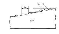
前記の中で好ましい異種基板としては、サファイアであり、更に好ましくはサファイアのC面である。また、サファイアのC面がステップ状にオフアングルされ、オフアングル角θ(図3に示されるθ)が0.1°〜0.3°の範囲のものを用いると、ELOG成長して得られる窒化物半導体内部の微細なクラックの発生を防止でき、よりいっそう好ましい。オフアングル角θが0.1°未満であるとELOG成長させた窒化物半導体の内部に微細なクラックが発生しやすくなる傾向があり、オフアングル角θが0.1°以上であるとその上に構成されるレーザ素子の特性を安定させることができる。また、オフアングル角が0.3°を超えると、ELOG成長させた窒化物半導体の表面がステップ状になり、その上に素子を構成すると、各半導体層においてステップが若干強調され、素子のショート及びしきい値上昇を招き好ましくない。
【0037】
前記のようなステップ状にオフアングルされたサファイア等の異種基板上に、保護膜を、直接又は一旦窒化物半導体を成長させてから、部分的(例えば、異種基板表面が一定間隔で露出するように)に形成する。
保護膜としては、保護膜表面に窒化物半導体が成長しないかまたは成長しにくい性質を有する種々の材料を用いることができ、例えば酸化ケイ素(SiOX)、窒化ケイ素(SiXNY)、酸化チタン(TiOX)、酸化ジルコニウム(ZrOX)等の酸化物、窒化物、またこれらの多層膜、さらには1200℃以上の融点を有する金属等を用いることができる。好ましい保護膜材料としては、SiO2及びSiNが挙げられる。
【0038】
保護膜材料を窒化物半導体等の表面に形成する方法としては、例えば蒸着、スパッタ、CVD等の気相成膜技術を用いることができる。
また、部分的(選択的)に形成する方法として、フォトリソグラフィー技術を用いて所定の形状を有するフォトマスクを作製し、そのフォトマスクを介して、前記材料を気相成膜する方法を用いることができる。保護膜の形状は、特に限定されるものではないが、例えばドット、ストライプ、碁盤面状の形状で形成でき、好ましくはストライプ状の形状とし、そのストライプがオリエンテーションフラット面(サファイアのA面)に垂直になるように形成する。
【0039】
また、異種基板の表面のうち、保護膜を形成する表面積の割合は、保護膜が形成されていない部分の表面積より大きくすることが好ましく、このようにすると、成長させる窒化物半導体に発生する転位を防止することができ、良好な結晶性を有する窒化物半導体基板が得られる。
例えば、保護膜をストライプ形状に形成する場合の保護膜のストライプ幅は、保護膜が形成されていない部分(窓部)の幅を3とした時に、10以上になるようにすることが好ましい。この場合、保護膜のストライプ幅w1は、保護膜が形成されていない部分(窓部)の幅w2として、w1:w2=16〜18:3を満足するように設定することがさらに好ましい。保護膜をストライプ形状に形成する場合、保護膜のストライプ幅と窓部の幅を前記の関係に設定すると、窒化物半導体が保護膜を覆い易くなり、且つ転位を効果的に防止することができる。保護膜のストライプ幅としては、例えば6〜27μm、好ましくは11〜24μmとして、窓部の幅としては、例えば2〜5μm、好ましくは2〜4μmとする。
【0040】
また、ELOG成長して得られる窒化物半導体上に素子を構成し、p型窒化物半導体層にリッジ形状のストライプ200を形成する場合、リッジ形状のストライプ200が、ストライプ状の保護膜の上であり、かつその中心線(長手方向に平行な中心線)上を避けて形成されていることが好ましく、このようにすると、しきい値を低下させることができ、素子の信頼性を向上させることができる。すなわち、保護膜上部に位置する窒化物半導体の結晶性が、窓部上部等に比較して良好であり、また、保護膜の中心線上付近は、窓部から成長した隣接する窒化物半導体同士が横方向の成長によって接合する部分でありこのような接合箇所に空隙の生じる場合があり、この空隙の上部にリッジ形状のストライプ200が形成されると、レーザ素子の動作中に空隙から転位が伝播し易くなり、素子の信頼性を劣化させる恐れがあるからである。
【0041】
また、保護膜は、異種基板に直接形成されてもよいが、異種基板上に低温成長のバッファ層101を形成させ、更にその上に高温成長の窒化物半導体からなるバッファ層102を成長させた上に、形成することが好ましく、このようにすると、転位の少ないより結晶性に優れた窒化物半導体基板を成長させることができる。
また、本発明に係る窒化物半導体発光素子を形成するために用いることができる基板は、上述したELOG成長させた窒化物半導体基板に限定されるものではない。本発明では、たとえば、サファイア基板の上にアンドープのGaNを数μmから数十μmの膜厚で成長させた下地層として成長させ、その上に素子を構成するようにしてもよい。
また、ELOG成長に用いる低温成長のバッファ層101としては、例えばAlN、GaN、AlGaN、及びInGaN等のいずれかを900℃以下200℃以上の温度で、膜厚数十オングストローム〜数百オングストロームで成長させたものを用いることができる。これらのバッファ層は、異種基板と比較的高温で成長される窒化物半導体層との間の格子定数不整を緩和することができ、成長させる層におれる転位の発生を防止することができる。
【0042】
高温成長の窒化物半導体からなるバッファ層102としては、アンドープのGaN、n型不純物をドープしたGaN、またSiをドープしたGaNを用いることができ、好ましくはアンドープのGaNを用いる。またこれらの窒化物半導体は、高温、具体的には900℃〜1100℃、好ましくは1050℃でバッファ層101上に成長される。本発明において、このバッファ層102の膜厚は特に限定されるものではないが、例えば1〜20μm、好ましくは2〜10μmとする。
【0043】
次に保護膜を形成した上に、窒化物半導体をMOCVD等により、ELOG成長させて窒化物半導体基板1を得る。この場合、成長させる窒化物半導体としては、アンドープのGaN又は不純物(例えばSi、Ge、Sn、Be、Zn、Mn、Cr、及びMg)をドープしたGaNを用いることができる。成長温度としては、例えば900℃〜1100℃、より具体的には1050℃付近の温度で成長させる。不純物がドープされていると成長層おける転位の発生を抑制することができ、好ましい。
【0044】
このELOG成長では、成長初期において、成長速度をコントロールし易いMOCVD(有機金属化学気相成長法)等で成長させ、保護膜がELOG成長の窒化物半導体で覆われた後の成長をHVPE(ハライド気相成長法)等で成長させてもよい。
以上のようにして、本実施の形態では、ELOG成長により窒化物半導体基板1を異種基板上に形成する。
【0045】
(窒化物半導体基板1上の各窒化物半導体層の形成)
本実施の形態では、まず、n型コンタクト層2を窒化物半導体基板1上に成長させる。n型コンタクト層2としては、n型不純物(好ましくはSi)がドープされたAlaGa1−aN(0<a<1)を成長させる。n型コンタクト層2として、好ましくはaが0.01〜0.05に設定されたAlaGa1−aNを成長させる。n型コンタクト層2をAlを含む3元混晶で形成すると、窒化物半導体基板1に微細なクラックが発生していても、微細なクラックの伝播を防止することができ、更に従来の問題点であった窒化物半導体基板1とn型コンタクト層2との格子定数及び熱膨張係数の相違によるn型コンタクト層への微細なクラックの発生を防止することができ好ましい。n型不純物のドープ量は、1×10¹⁸/cm3〜5×1018/cm3とする。このn型コンタクト層2にはn電極21が形成される。n型コンタクト層2の膜厚は、1〜10μmとする。
また、本実施の形態では、窒化物半導体基板1とn型コンタクト層2との間に、アンドープのAlaGa1−aN(0<a<1)を成長させてもよく、このアンドープの層を成長させるとn型コンタクト層2の結晶性を良好とでき、寿命特性を向上させることができる。この場合、アンドープn型コンタクト層の膜厚は、数μmとする。
【0046】
次に、クラック防止層3をn型コンタクト層2上に成長させる。クラック防止層3としては、SiドープのIngGa1−gN(0.05≦g≦0.2)を成長させ、gが0.05〜0.08に設定されたIngGa1−gNを成長させることが好ましい。このクラック防止層3をn型コンタクト層2上に形成すると、素子内のクラックの発生を防止することができ、好ましい。Siのドープ量としては、5×10¹⁸/cm3である。しかしながら、本発明では、クラック防止層3を省略してもよい。
【0047】
また、クラック防止層3を成長させる際に、Inの混晶比を大きく(x≧0.1)することが好ましく、このようにすると、クラック防止層3がn型クラッド層4から漏れ出した、活性層6で発生された光を吸収することができ、レーザ光のファーフィールドパターンの乱れを防止することができる。
このクラック防止層の膜厚は、例えば、0.05〜0.3μmのそれ自身の結晶性が損なわれない程度の厚みとする。
【0048】
次に、n型クラッド層4をクラック防止層3上に成長させる。n型クラッド層4は、AleGa1−eN(0.12≦e<0.15)を含む窒化半導体を有する多層膜の層として形成される。多層膜とは、互いに組成が異なる窒化物半導体層を積層した多層膜構造を示し、例えば、AleGa1−eN(0.12≦e<0.15)層と、このAleGa1−eNと組成の異なる窒化物半導体、例えばAlの混晶比の異なるもの、Inを含んでなる3元混晶のもの、又はGaN等からなる層とを組み合わせて積層してなるものである。この中で好ましい組み合わせとしては、AleGa1−eNとGaNとを積層してなる多層膜である。このようにすると、同一温度で結晶性の良い窒化物半導体層が積層できる。より好ましい多層膜としては、アンドープのAleGa1−eNとn型不純物(例えばSi)ドープのGaNとを組み合わせて積層したものである。この場合、n型不純物は、AleGa1−eNにドープされてもよい。n型不純物のドープ量は、4×10¹⁸/cm3〜5×1018/cm3である。n型不純物がこの範囲でドープされていると抵抗率を低くでき且つ結晶性を損なうことなくn型クラッド層4を形成することができる。
【0049】
この多層膜は、単一層の膜厚が100オングストローム以下、好ましくは70オングストローム以下、さらに好ましくは40オングストローム以下であって、好ましくは10オングストローム以上の膜厚の窒化物半導体層を積層することにより構成する。単一の膜厚が100オングストローム以下であるとn型クラッド層が超格子構造となり、Alを含有しているにもかかわらず、クラックの発生を防止でき結晶性を良好にすることができる。また、n型クラッド層4の総膜厚は、0.7〜2μmである。
【0050】
またn型クラッド層の全体の平均組成は、その平均組成をAlkGa1−kNで表したときに、kを0.05〜0.1とすることが好ましい。Alの含有率がこの範囲であると、クラックを発生させないように形成でき、且つ充分にレーザ導波路との屈折率の差を得ることができる。
次に、n型ガイド層5をn型クラッド層4上に成長させる。n型ガイド層5としては、アンドープのGaNからなる窒化物半導体を成長させる。n型ガイド層5の膜厚は、0.1〜0.07μmに設定することが好ましく、このようにすると、しきい値を低下させることができる。
また、n型ガイド層4をアンドープとすることが好ましく、これによって、レーザ導波路内の伝搬損失を減少させることができ、かつしきい値を低くすることができる。
【0051】
次に、活性層6をn型ガイド層5上に成長させる。本実施の形態において、活性層は、IncGa1−cN(0≦c<1)を含んでなる多重量子井戸構造を有する。活性層6において、井戸層は、cが0.1〜0.2のIncGa1−cNとし、障壁層は、cが0〜0.01のIncGa1−cNとする。
また活性層6を構成する井戸層及び障壁層のいずれか一方または両方に不純物をドープしてもよい。この場合、障壁層に不純物をドープさせると、しきい値を低下させることができ好ましい。
井戸層の膜厚としては、30〜60オングストロームであり、障壁層の膜厚としては、90〜150オングストロームである。
【0052】
多重量子井戸構造の活性層6は、障壁層から始まり井戸層で終わっても、障壁層から始まり障壁層で終わっても、井戸層から始まり障壁層で終わっても、また井戸層から始まり井戸層で終わってもよい。好ましくは障壁層から始まり、井戸層と障壁層とのペアを2〜5回繰り返してなるもの、好ましくは井戸層と障壁層とのペアを3回繰り返してなるものがしきい値を低くし寿命特性を向上させるのに好ましい。
【0053】
次に、p型キャップ層7を活性層6上に成長させる。p型キャップ層7としては、MgドープのAldGa1−dN(0<d≦1)からなる少なくとも2層を成長させて構成する。このp型キャップ層7の混晶比は、好ましくはdが0.1以上0.5以下の範囲に設定する。本発明におけるp型キャップ層を構成する第1のp型窒化物半導体層、第2のp型窒化物半導体層については、上記範囲の混晶比が適用されるが、各層について詳しくは後述するとおりである。
また、p型キャップ層7全体の膜厚は、10オングストローム以上1000オングストローム以下、好ましくは20オングストローム以上400オングストローム以下に設定する。p型キャップ層7全体の膜厚をこのような範囲に設定するのは、次のような理由によるものである。
すなわち、p型キャップ層7をAlGaN層とした場合、キャリア閉じ込め機能を効果的に発揮させることができるが、AlGaN層はAlを含まない窒化ガリウム系半導体に比較してバルク抵抗が高いものである。従って、p型キャップ層を形成したことによる発光素子における抵抗値の上昇を抑える必要があるために、1000オングストローム以下、好ましくは400オングストローム以下に設定する。
また、このp型キャップ層7の本来の機能は、上述のキャリア閉じ込め機能であり、その機能を効果的に発揮させるために、その膜厚を10オングストローム以上、好ましくは20オングストローム以上に設定する。
従って、膜厚が上記範囲であると、活性層6内にキャリアを効果的に閉じ込めることができ、且つバルク抵抗も低く抑えることができる。
【0054】
またp型キャップ層7のMgのドープ量は、1×10¹⁹/cm3〜1×1021/cm3とする。ドープ量をこの範囲に設定すると、バルク抵抗を低下させることに加えて、後述のアンドープで成長させるp型ガイド層にMgが拡散され、比較的薄い層であるp型ガイド層8にMgを1×1016/cm3〜1×1018/cm3の範囲で含有させることができる。
【0055】
ここで特に、本実施の形態においてp型キャップ層7は、AlaGa1−aNからなる第1のp型窒化物半導体層7aと、その上にAlbGa1−bNからなる第2のp型窒化物半導体層7bの2層で構成した。しかしながら、本発明はこれに限られるものではなく、2以上の層としてもよく、また、例えば、第2のp型窒化物半導体層7bを複数の層を積層することにより形成してもよい。
【0056】
また、各層のAl混晶比は特に限定されるものではない。しかし、AlaGa1−aN層で表される第1のp型窒化物半導体層7aにおいては、Al混晶比aは、0以上であれば、活性層の分解を効果的に抑制することができる。この機能を発揮させるためには、好ましくはa>0のAlaGa1−aN層とすると、窒化物半導体の中でも比較的高融点で化学的に安定な層を、活性層に近い方に(好ましくは接する)設けることができ、活性層の分解をより効果的に抑制することができる。また、本発明においては、第1のp型窒化物半導体層7a及び第2のp型窒化物半導体層7bの各Al混晶比a、bを、好ましくは0.1より大きく、更に好ましくは0.2より大きくすることで、活性層との間に良好なオフセットをとる(電位障壁を形成する)ことができ、キャリアのオーバフローのない良好なキャリア注入を実現することができる。この時、第1のp型窒化物半導体層7aと第2のp型窒化物半導体層7bとは、同一の組成、すなわちa=bとすることが好ましく、このような条件下では、製造において各ソースガス、不純物ガスの供給量の調整等が容易にできかつ制御性を高くできるので、第1のp型窒化物半導体層及び第2のp型窒化物半導体層を安定して、精度よく成長させることができる。
【0057】
次に、第1のp型窒化物半導体層7a、第2のp型窒化物半導体層7bの成長条件について説明する。
成長温度としては、第1のp型窒化物半導体層よりも高い温度で第2のp型窒化物半導体層を成長させることが好ましい。
特に、第1のp型窒化物半導体層の具体的な成長温度は850〜950℃程度、活性層を成長させる温度と同様の温度に設定すると、Inを含む活性層6の分解を防止することができ好ましい。
そして、第2のp型窒化物半導体層の成長温度は、例えば活性層の成長温度より100℃程度高いの温度に設定することが好ましく、これによりより良好な結晶性を有するAlGaN層を形成することができる。
【0058】
さらに、第1のp型窒化物半導体層と第2のp型窒化物半導体層の成長時の雰囲気は、異なる雰囲気とすることが好ましい。すなわち、第1のp型窒化物半導体は、活性層とほぼ同じ雰囲気で成長させることが好ましく、こうすることで、活性層の分解を防しできる。また、第2のp型窒化物半導体は、良好なオフセットを形成するために好ましい雰囲気で成長させる。このようにすると、2つの層の結晶成長形態の違いにより、第1のp型窒化物半導体層は活性層の分解を防ぐ層、第2のp型窒化物半導体は良好なオフセットの実現を担う層とでき、各層にそれぞれ特有の機能を持たせることができる。具体的には、第1のp型窒化物半導体層の成長雰囲気はN2とし、第2のp型窒化物半導体層の成長雰囲気はH2とすることで、それぞれ上述の機能を有する層が形成できるため、得られる素子は良好な発光特性を有する。
【0059】
またp型キャップ層7を前記少なくとも2層から構成する場合の各層の膜厚は、p型キャップ層を形成したことによる発光素子のVf(順方向電圧)の上昇を小さく抑えるために、第1のp型窒化物半導体層は10〜100オングストロームの範囲、第2のp型窒化物半導体層は10〜300オングストロームの範囲に設定することが好ましい。また、Vfの上昇をより小さく抑えるために、第1のp型窒化物半導体層を10〜30Åの範囲、第2のp型窒化物半導体層を10〜100Åオングストロームの範囲に設定することがさらに好ましい。
次に、p型ガイド層8をp型キャップ層7上に成長させる。p型ガイド層8は、アンドープのGaNからなる窒化物半導体層を成長させて形成する。膜厚は0.1〜0.07μmとすることが好ましく、この範囲の膜厚にするとしきい値を低くすることができる。また上述のように、p型ガイド層8はアンドープ層として成長させるが、p型キャップ層7にドープされているMgが拡散して、1×10¹⁶/cm3〜1×1018/cm3の範囲でMgが含有される。
【0060】
次に、p型クラッド層9をp型ガイド層8上に成長させる。p型クラッド層9としては、AlfGa1−fN(0<f≦1)を含んでなる窒化物半導体層、好ましくはAlfGa1−fN(0.05≦f≦0.15)を含んでなる窒化物半導体層を有する多層膜層とすることが好ましい。多層膜とは、互いに組成が異なる窒化物半導体層を積層した多層膜構造を有する層であり、例えば、AlfGa1−fN層と、AlfGa1−fNと組成の異なる窒化物半導体、例えばAlの混晶比の異なるもの、Inを含んでなる3元混晶のもの、又はGaN等からなる層とを組み合わせて積層してなるものである。この中で特に、AlfGa1−fNとGaNとを組み合わせて積層した多層膜とすると、同一温度で結晶性の良い窒化物半導体層が積層できるので好ましい。より好ましい多層膜としは、アンドープのAlfGa1−fNとp型不純物(例えばMg)ドープのGaNとを積層してなる組み合わせである。p型不純物は、AlfGa1−fNにドープされてもよい。p型不純物のドープ量は、1×10¹⁷/cm3〜1×1019/cm3である。p型不純物がこの範囲でドープされていると結晶性を損なわない程度のドープ量で且つバルク抵抗を低くできる。
【0061】
この多層膜において、単一層の膜厚が100オングストローム以下、好ましくは70オングストローム以下、さらに好ましくは40オングストローム以下とし、好ましくは10オングストローム以上の膜厚の窒化物半導体層を積層して構成する。単一の膜厚が100オングストローム以下であるとn型クラッド層が超格子構造となり、Alを含有しているにもかかわらず、クラックの発生を防止できn型クラッド層全体の結晶性を良好にすることができる。
p型クラッド層9の総膜厚としては、0.4〜0.5μmとすることが好ましく、この範囲に設定すると順方向電圧(Vf)を低減することができる。
【0062】
またp型クラッド層9の全体のAlの平均組成は、AlsGa1−sNで表したときに、sが0.05〜0.1の範囲に設定することが好ましく、このようにすると、クラックの発生を抑制し且つレーザ導波路との間に良好な屈折率差が得られる。
次に、p型コンタクト層10をp型クラッド層9上に成長させる。p型コンタクト層は、MgドープのGaNからなる窒化物半導体層を成長させた層である。膜厚は10〜200オングストロームに設定する。Mgのドープ量は1×10¹⁹/cm3〜1×1022/cm3とする。このよう膜厚とMgのドープ量を調整することにより、p型コンタクト層のキャリア濃度を高くでき、p電極との間に良好なオーミック接触を形成することができる。
【0063】
本発明の素子において、リッジ形状のストライプ200は、p型コンタクト層から所定の深さまでエッチングすることにより形成する。本実施の形態では、例えば、図1に示すようなp型コンタクト層10からp型クラッド層9の途中までエッチングしてなるリッジ形状のストライプ200、又はp型コンタクト層10からn型コンタクト層2までエッチングしてなるリッジ形状のストライプ200などの種々のリッジ形状のストライプ200を適用することができる。
【0064】
エッチングして形成されたリッジ形状のストライプ200の側面やその側面に連続した窒化物半導体層の平面に、例えば図1に示すように、レーザ導波路領域の屈折率より小さい値を有する絶縁膜62が形成されている。ストライプの側面等に形成される絶縁膜としては、例えば、屈折率が約1.6〜2.3付近の値を有する、Si、V、Zr、Nb、Hf、Taよりなる群から選択された少なくとも一種の元素を含む酸化物や、BN、AlN等が挙げられ、好ましくは、Zr及びHfの酸化物のいずれか1種以上の元素や、BNである。
【0065】
さらにこの絶縁膜62を介してリッジ形状のストライプ200の最上層にあるp型コンタクト層10の表面にp電極が形成される。
エッチングして形成されるリッジ形状のストライプ200の幅としては、0.5〜4μm、好ましくは1〜3μmとする。リッジ形状のストライプ200の幅をこの範囲に設定すると、水平横モードを単一モードにできる。
また、p型クラッド層9とレーザ導波路領域との界面より深くエッチングをすることにより、リッジ形状のストライプ200を形成すると、アスペクト比を1に近づけることができるので好ましい。
【0066】
以上のように、リッジ形状のストライプ200のエッチング量や、ストライプ幅、さらにストライプの側面の絶縁膜の屈折率などを、単一モードのレーザ光が得られ、さらにアスペクト比を円形に近づけるように設定することが好ましく、レーザビームやレンズ設計を容易にできる。
また本発明の素子において、p電極やn電極等は従来公知の種々のものを適宜選択して用いることができる。
【0067】
また、本発明は実施の形態で説明した層構成に限定されるものではなく、以下のような変形も可能である。
変形例
実施の形態の窒化物半導体発光素子では、p型キャップ層7の一部として、活性層6の分解を防止する第1のp型窒化物半導体層7aを形成したが、本発明ではp型クラッド層7と活性層の間に少なくとも1つの第1のp型窒化物半導体層を形成するようにしてもよい。
すなわち、本発明に係る窒化物半導体発光素子において、p型クラッド層7と活性層の間に、p型クラッド層7の成長温度より低い成長温度でp型クラッド層よりバンドギャップの大きい第1のp型窒化物半導体層を形成するようにすると、活性層の結晶品質を良好に保ちかつ結晶性の良いp型クラッド層を形成することが可能となる。
また、この変形例において、第1のp型窒化物半導体層はバンドギャップをクラッド層より大きく設定しているので、一定のキャリア閉じ込め機能を発揮させることができる。
したがって、本変形例の窒化物半導体発光素子は、従来例に比較して、出力及び素子の信頼性を高くできる。
【0068】
【実施例】
以下に本発明の一実施の形態である実施例を示す。しかし本発明はこれに限定されない。
また、本実施例はMOVPE(有機金属気相成長法)について示すものであるが、本発明の方法は、MOVPE法に限るものではなく、例えばHVPE(ハライド気相成長法)、MBE(分子線気相成長法)等、窒化物半導体を成長させるのに知られている全ての方法を適用できる。
【0069】
[実施例1]
実施例1として、図1に示される本発明の一実施の形態である窒化物半導体レーザ素子を製造する。
異種基板として、図3に示すようにステップ状にオフアングルされたC面を主面とし、オフアングル角θ=0.15°、ステップ段差およそ20オングストローム、テラス幅Wおよそ800オングストロームであり、オリフラ面をA面とし、ステップがA面に垂直であるサファイア基板を用意する。
【0070】
このサファイア基板を反応容器内にセットし、温度を510℃にして、キャリアガスに水素、原料ガスにアンモニアとTMG(トリメチルガリウム)とを用い、サファイア基板上にGaNよりなる低温成長のバッファ層を200オングストロームの膜厚で成長させる。
バッファ層成長後、TMGのみ止めて、温度を1050℃まで上昇させ、1050℃になったら、原料ガスにTMG、アンモニア、シランガスを用い、アンドープのGaNからなる高温成長のバッファ層を5μmの膜厚で成長させる。
【0071】
次に、高温成長のバッファ層を積層したウェーハ上にストライプ状のフォトマスクを形成し、CVD装置によりストライプ幅18μm、窓部の幅3μmのSiO2よりなる保護膜を0.1μmの膜厚で形成する。保護膜のストライプ方向はサファイアA面に対して垂直な方向である。
保護膜形成後、ウェーハを反応容器に移し、1050℃にて、原料ガスにTMG、アンモニアを用い、アンドープのGaNよりなる窒化物半導体層を15μmの膜厚で成長させ窒化物半導体基板1とする。
得られた窒化物半導体を窒化物半導体基板1として以下の素子構造を積層成長させる。
【0072】
(アンドープn型コンタクト層)[図1には図示されていない]
窒化物半導体基板1上に、1050℃で原料ガスにTMA(トリメチルアルミニウム)、TMG、アンモニアガスを用いアンドープのAl0.05Ga0.95Nよりなるn型コンタクト層を1μmの膜厚で成長させる。
【0073】
(n型コンタクト層2)
次に、同様の温度で、原料ガスにTMA、TMG及びアンモニアガスを用い、不純物ガスにシランガス(SiH4)を用い、Siを3×10¹⁸/cm3ドープしたAl0.05Ga0.95Nよりなるn型コンタクト層2を3μmの膜厚で成長させる。
成長されたn型コンタクト層2には、微細なクラックが発生しておらず、微細なクラックの発生が良好に防止されている。また、窒化物半導体基板1に微細なクラックが生じていても、n型コンタクト層2を成長させることで微細なクラックの伝播を防止でき結晶性の良好な素子構造を成長さることができる。結晶性の改善は、n型コンタクト層2のみの場合より、前記のようにアンドープn型コンタクト層を成長させることによりより良好となる。
【0074】
(クラック防止層3)
次に、温度を800℃にして、原料ガスにTMG、TMI(トリメチルインジウム)及びアンモニアを用い、不純物ガスにシランガスを用い、Siを5×10¹⁸/cm3ドープしたIn0.08Ga0.92Nよりなるクラック防止層3を0.15μmの膜厚で成長させる。
【0075】
(n型クラッド層4)
次に、温度を1050℃にして、原料ガスにTMA、TMG及びアンモニアを用い、アンドープのAl0.14Ga0.86NよりなるA層を25オングストロームの膜厚で成長させ、続いて、TMAを止め、不純物ガスとしてシランガスを用い、Siを5×10¹⁸/cm3ドープしたGaNよりなるB層を25オングストロームの膜厚で成長させる。そして、この操作をそれぞれ160回繰り返してA層とB層の積層し、総膜厚8000オングストロームの多層膜(超格子構造)よりなるn型クラッド層4を成長させる。
【0076】
(n型ガイド層5)
次に、同様の温度で、原料ガスにTMG及びアンモニアを用い、アンドープのGaNよりなるn型ガイド層を0.075μmの膜厚で成長させる。
(活性層6)
次に、温度を800℃にして、原料ガスにTMI、TMG及びアンモニアを用い、不純物ガスとしてシランガスを用い、キャリアガスとしてN2を用い、反応容器内をN2雰囲気として、Siを5×10¹⁸/cm3ドープしたIn0.01Ga0.99Nよりなる障壁層を100オングストロームの膜厚で成長させる。続いて、シランガスを止め、アンドープのIn0.11Ga0.89Nよりなる井戸層を50オングストロームの膜厚で成長させる。この操作を3回繰り返し、最後に障壁層を積層した総膜厚550オングストロームの多重量子井戸構造(MQW)の活性層6を成長させる。
【0077】
(p型キャップ層7)
次に、同様の温度、同様の雰囲気(N2)で、原料ガスにTMA、TMG及びアンモニアを用い、不純物ガスとしてCp2Mg(シクロペンタジエニルマグネシウム)を用い、Mgを1×10¹⁹/cm3ドープしたAl0.4Ga0.6Nよりなる第1のp型窒化物半導体層7aを、膜厚20Åで成長させる。次に、キャリアガスをH2にして、H2雰囲気とし、960℃まで上昇させた後、同様にしてMgを1×1019/cm3ドープしたAl0.4Ga0.6Nよりなる第2のp型窒化物半導体層7bを、膜厚70Åで成長させる。この第1のp型窒化物半導体層と、第2のp型窒化物半導体層とでもって、p型キャップ層7とし、層膜厚90Åで形成する。
【0078】
(p型ガイド層8)
次に、温度を1050℃にして、原料ガスにTMG及びアンモニアを用い、アンドープのGaNよりなるp型ガイド層8を0.075μmの膜厚で成長させる。
このp型ガイド層8は、アンドープとして成長させるが、p型キャップ層7からのMgの拡散により、Mg濃度が5×10¹⁶/cm3となりp型を示す。
【0079】
(p型クラッド層9)
次に、同様の温度で、原料ガスにTMA、TMG及びアンモニアを用い、アンドープのAl0.1Ga0.9NよりなるA層を25オングストロームの膜厚で成長させ、続いて、TMAを止め、不純物ガスとしてCp2Mgを用い、Mgを5×10¹⁸/cm3ドープしたGaNよりなるB層を25オングストロームの膜厚で成長させる。そして、この操作をそれぞれ100回繰り返してA層とB層の積層し、総膜厚5000オングストロームの多層膜(超格子構造)よりなるp型クラッド層9を成長させる。
【0080】
(p型コンタクト層10)
次に、同様の温度で、原料ガスにTMG及びアンモニアを用い、不純物ガスとしてCp2Mgを用い、Mgを1×10²⁰/cm3ドープしたGaNよりなるp型コンタクト層10を150オングストロームの膜厚で成長させる。
反応終了後、反応容器内において、ウエハを窒素雰囲気中、700℃でアニーリングを行い、p型層を更に低抵抗化する。
アニーリング後、ウエハを反応容器から取り出し、最上層のp側コンタクト層の表面にSiO2よりなる保護膜を形成して、RIE(反応性イオンエッチング)を用いSiCl4ガスによりエッチングし、図4に示すように、n電極を形成すべきn側コンタクト層2の表面を露出させる。
【0081】
次に図4(a)に示すように、最上層のp側コンタクト層10のほぼ全面に、PVD装置により、Si酸化物(主として、SiO2)よりなる第1の保護膜61を0.5μmの膜厚で形成した後、第1の保護膜61の上に所定の形状のマスクをかけ、フォトレジストよりなる第3の保護膜63を、ストライプ幅1.8μm、厚さ1μmで形成する。
次に、図4(b)に示すように第3の保護膜63形成後、RIE(反応性イオンエッチング)装置により、CF4ガスを用い、第3の保護膜63をマスクとして、前記第1の保護膜をエッチングして、ストライプ状とする。その後エッチング液で処理してフォトレジストのみを除去することにより、図4(c)に示すようにp側コンタクト層10の上にストライプ幅1.8μmの第1の保護膜61が形成できる。
【0082】
さらに、図4(d)に示すように、ストライプ状の第1の保護膜61形成後、再度RIEによりSiCl4ガスを用いて、p側コンタクト層10、およびp側クラッド層9をエッチングして、ストライプ幅1.8μmのリッジ形状のストライプ200を形成する。但し、リッジ形状のストライプ200は、図1に示すように、ELOG成長を行う際に形成した保護膜の上部で且つ保護膜の中心部分を避けるように形成される。
【0083】
リッジストライプ形成後、ウェーハをPVD装置に移送し、図4(e)に示すように、Zr酸化物(主としてZrO2)よりなる第2の保護膜62を、第1の保護膜61の上と、エッチングにより露出されたp側クラッド層9の上に0.5μmの膜厚で連続して形成する。このようにZr酸化物を形成すると、p−n面の絶縁をとるためと、横モードの安定を図ることができ好ましい。
次に、ウェーハをフッ酸に浸漬し、図4(f)に示すように、第1の保護膜61をリフトオフ法により除去する。
【0084】
次に図4(g)に示すように、p側コンタクト層10の上の第1の保護膜61が除去されて露出したそのp側コンタクト層の表面にNi/Auよりなるp電極20を形成する。但しp電極20は100μmのストライプ幅として、この図に示すように、第2の保護膜62の上に渡って形成する。
第2の保護膜62形成後、図1に示されるように露出させたn側コンタクト層2の表面にはTi/Alよりなるn電極21をストライプと平行な方向で形成する。
【0085】
以上のようにして、n電極とp電極とを形成したウェーハのサファイア基板を研磨して70μmとした後、ストライプ状の電極に垂直な方向で、基板側からバー状に劈開し、劈開面(11−00面、六角柱状の結晶の側面に相当する面=M面)に共振器を作製する。共振器面にSiO2とTiO2よりなる誘電体多層膜を形成し、最後にp電極に平行な方向で、バーを切断して図1に示すようなレーザ素子とする。なお共振器長は300〜500μmとすることが望ましい。
得られたレーザ素子をヒートシンクに設置し、それぞれの電極をワイヤーボンディングして、室温でレーザ発振を試みた。
【0086】
その結果、室温においてしきい値2.5kA/cm2、しきい値電圧5Vで、発振波長400nmの連続発振が確認され、室温で1万時間以上の寿命を示す。
更には、30mW駆動時において、比較例1に比べてVfが0.5Vも大きく低下した。このことは、前記p型キャップ層が、上述した2層構造を少なくとも有することで、Ithの上昇がなく、素子寿命を向上させることを示す結果となった。なお、2.0mA時では、Vfは0.1〜0.2V程度の低下を示すが、本発明の発光素子は、高出力時に従来のものから大きくその素子特性が向上していることがわかる。
【0087】
[比較例1]
実施例1において、p型キャップ層7を以下のように1層から構成させる他は同様にして窒化物半導体レーザ素子を作製する。
(p型キャップ層7)
活性層を成長させた後、同温度(800℃)、同雰囲気(N2雰囲気)にて、原料ガスにTMA、TMG及びアンモニアを用い、不純物ガスとしてCp2Mg(シクロペンタジエニルマグネシウム)を用い、Mgを5×10¹⁸/cm3ドープしたAl0.4Ga0.6Nよりなるp型キャップ層7を、膜厚100Åで成長させる。
得られたレーザ素子は、実施例1と比べて、Vfが高く、素子寿命も劣るものであった。
【0088】
[実施例2]
キャリアガスにN2、原料ガスにTMA、TMG、アンモニア、不純物ガスにCp2Mg(シクロペンタジエニルマグネシウム)を用い、温度800℃で、すなわち、活性層成長時とほぼ同様の温度、同様の雰囲気で、膜厚30ÅのMgを1×10¹⁹/cm3ドープしたAl0.4Ga0.6Nよりなる第1のp型窒化物半導体層7aを成長させ、キャリアガスをH2にして水素雰囲気下で、960℃に昇温した後、膜厚100ÅでMgを1×1019/cm3ドープしたAl0.4Ga0.6Nを成長させ、この2層でp型キャップ層を形成する他は、実施例1と同様にして、レーザ素子を形成する。得られるレーザ素子は、実施例1とほぼ同様に良好な素子信頼性を有するものであり、出力特性に関しても同程度のVfで、閾値電流Ithの上昇もなく、高出力での連続発振が可能な素子であった。
【0089】
また、上記第1のp型窒化物半導体層、第2のp型窒化物半導体層の膜厚を、それぞれ100Å、100Å、更にはそれぞれ100Å、400Åとして、素子特性の変化を調べる。各層の膜厚が100Åでは、素子特性に大きな変化はないものの、Vfの上昇が現れ始め、出力特性が僅かに劣る傾向を示し、それぞれの膜厚が100Å、400Åでは、その傾向が顕著となり、膜厚が増えたことによるVfの上昇、これによる閾値電流の上昇が観測された。
【0090】
[実施例3]
第1のp型窒化物半導体層の組成をAl0.2Ga0.8Nとする他は、実施例1と同様にして、レーザ素子を形成する。得られるレーザ素子は、実施例1とほぼ同程度の出力特性を有し、これは第1のp型窒化物半導体層が活性層との電位障壁をとること、電子閉じ込めることに、第2のp型窒化物半導体層ほど寄与していないことを示すものであり、それよりも、上層の第2のp型窒化物半導体層の良好な結晶成長、活性層の保護への寄与が大きいことを示すものである。このため、素子信頼性、特に素子寿命についても、実施例1とほぼ同様に、良好な寿命特性を示すものであった。
【0091】
[実施例4]
図5を元に実施例5について説明する。
サファイア(C面)よりなる基板100をMOVPEの反応容器内にセットし、水素を流しながら、基板の温度を1050℃まで上昇させ、基板のクリーニングを行う。
(バッファ層101)
続いて、温度を510℃まで下げ、キャリアガスに水素、原料ガスにアンモニアとTMG(トリメチルガリウム)とを用い、基板100上にGaNよりなるバッファ層101を約150オングストロームの膜厚で成長させる。
【0092】
(アンドープGaN層103)
バッファ層101成長後、TMGのみ止めて、温度を1050℃まで上昇させる。1050℃になったら、同じく原料ガスにTMG、アンモニアガスを用い、アンドープGaN層103を1.5μmの膜厚で成長させる。
【0093】
(n型コンタクト層104)
続いて1050℃で、同じく原料ガスにTMG、アンモニアガス、不純物ガスにシランガスを用い、Siを4.5×10¹⁸/cm3ドープしたGaNよりなるn型コンタクト層104を2.25μmの膜厚で成長させる。
【0094】
(n型クラッド層105)
次にシランガスのみを止め、1050℃で、TMG、アンモニアガスを用い、アンドープGaN層を75オングストロームの膜厚で成長させ、続いて同温度にてシランガスを追加しSiを4.5×10¹⁸/cm3ドープしたGaN層を25オングストロームの膜厚で成長させる。このようにして、75オングストロームのアンドープGaN層からなるA層と、SiドープGaN層を有する25オングストロームのB層とからなるペアを成長させる。そしてペアを25層積層して2500オングストローム厚として、超格子構造の多層膜よりなるn型第1多層膜層5を成長させる。
【0095】
(n型バッファ層106)
次に、同様の温度で、アンドープGaNよりなる第1の層を40オングストローム成長させ、次に温度を800℃にして、TMG、TMI、アンモニアを用い、アンドープIn0.13Ga0.87Nよりなる第2の層を20オングストローム成長させる。そしてこれらの操作を繰り返し、第2の層+第1の層の順で交互に10層づつ積層させ、最後にGaNよりなる第2の層を40オングストローム成長さた超格子構造の多層膜よりなるn型バッファ層106を640オングストロームの膜厚で成長させる。
【0096】
(活性層107)
次に、キャリアガスをN2に代えて窒素雰囲気として、アンドープGaNよりなる障壁層を200オングストロームの膜厚で成長させ、続いて温度を800℃にして、TMG、TMI、アンモニアを用いアンドープIn0.4Ga0.6Nよりなる井戸層を30オングストロームの膜厚で成長させる。そして障壁+井戸+障壁+井戸・・・・+障壁の順で障壁層を5層、井戸層を4層、交互に積層して、総膜厚1120オングストロームの多重量子井戸構造よりなる活性層107を成長させる。
【0097】
(p型キャップ層108)
活性層と同様に、キャリアガスとしてN2を用い活性層成長時とほぼ同様な雰囲気、温度の下、原料ガスとしてTMA、TMG、アンモニア、不純物ガスにCp2Mg(シクロペンタジエニルマグネシウム)を用い、膜厚20オングストロームのMgを1×10¹⁹/cm3ドープしたAl0.4Ga0.6Nよりなる第1のp型窒化物半導体層7aを成長させ、キャリアガスをH2に代えて水素雰囲気下で、960℃に昇温した後、膜厚60オングストロームでMgを1×1019/cm3ドープしたAl0.4Ga0.6Nを成長させ、この2層で膜厚80オングストロームのp型キャップ層を形成する。
【0098】
(p型多層膜クラッド層109)
次に、温度1050℃でTMG、TMA、アンモニア、Cp2Mg(シクロペンタジエニルマグネシウム)を用い、Mgを1×10²⁰/cm3ドープしたp型Al0.2Ga0.8Nよりなる第1の層を40オングストロームの膜厚で成長させ、続いて温度を800℃にして、TMG、TMI、アンモニア、Cp2Mgを用いMgを1×1020/cm3ドープしたIn0.03Ga0.97Nよりなる第2の層を25オングストロームの膜厚で成長させる。そしてこれらの操作を繰り返し、第1+第2の順で交互に5層ずつ積層し、最後に第1の層を40オングストロームの膜厚で成長させた超格子構造の多層膜よりなるp型多層膜クラッド層109を365オングストロームの膜厚で成長させる。
【0099】
(p型GaNコンタクト層110)
続いて1050℃で、TMG、アンモニア、Cp2Mgを用い、Mgを1×10²⁰/cm3ドープしたp型GaNよりなるp型コンタクト層110を700オングストロームの膜厚で成長させる。
反応終了後、温度を室温まで下げ、さらに窒素雰囲気中、ウェーハを反応容器内において、700℃でアニーリングを行い、p型層をさらに低抵抗化する。
アニーリング後、ウェーハを反応容器から取り出し、最上層のp型コンタクト層110の表面に所定の形状のマスクを形成し、RIE(反応性イオンエッチング)装置でp型コンタクト層側からエッチングを行い、図5に示すようにn型コンタクト層104の表面を露出させる。
【0100】
エッチング後、最上層にあるp型コンタクト層のほぼ全面に膜厚200オングストロームのNiとAuを含む透光性のp電極111と、そのp電極111の上にボンディング用のAuよりなるpパッド電極(図示せず)を0.5μmの膜厚で形成する。一方、エッチングにより露出させたn型コンタクト層104の表面にはWとAlを含むn電極112を形成してLED素子とした。
このLED素子は順方向電流20mAにおいて、520nmの純緑色発光を示し、Vfは3.5Vであった。このように、LED素子についても、良好なVfを示し、また素子寿命についてもレーザ素子と同様に、p型キャップ層が比較例1,2のような構造にあるLED素子に比べて、Vfの上昇が抑えられ高出力で、且つ良好な第2のp型窒化物半導体の成長に支えられ素子信頼性の高いものである。
【0101】
[比較例2]
p型キャップ層として、キャリアガスをH2として水素雰囲気下で、温度960℃で、Mgを1×10¹⁹/cm3ドープしたAl0.2Ga0.8Nを膜厚70Åで形成する他は、実施例1と同様にしてレーザ素子を得た。得られたレーザ素子は、実施例1に比べて、Vfは少し高くなるものの発振に大きな違いが出るほどではなかったが、素子寿命が極めて悪く、1万時間には遠く及ぶものではなく、素子断面を観察したところ、成長時乃至は駆動時に活性層が分解したことによるところが多きことがわかった。
【0102】
【発明の効果】
本発明は、第1のp型窒化物半導体層が活性層の分解、特にInの蒸発・分離を防止し、第2のp型窒化物半導体層が良好な結晶性でもって形成されるため、活性層との良好なオフセットをとることができ、結果として得られる発光素子は、Vfの低下、素子寿命の向上、の向上した素子が得られる。
【図面の簡単な説明】
【図1】図1は、本発明の一実施の形態である窒化物半導体レーザ素子を示す模式的断面図である。
【図2】図2は、サファイアの面方位を示すユニットセル図である。
【図3】図3は、オフアングルした異種基板の部分的な形状を示す模式的断面図である。
【図4】 図4は、リッジ形状のストライプ200を形成する一実施の形態である方法の各工程におけるウエハの部分的な構造を示す模式的断面図である。
【図5】 本発明に係る実施例5のLED素子の模式的断面図である。
【符号の説明】
1・・・窒化物半導体基板、
2・・・n型コンタクト層、
3・・・クラック防止層、
4・・・n型クラッド層、
5・・・n型ガイド層、
6・・・活性層、
7a・・・第1のp型窒化物半導体層、
7b・・・第2のp型窒化物半導体層、
7・・・p型キャップ層、
8・・・p型ガイド層、
9・・・p型クラッド層、
10・・・p型コンタクト層。[0001]
BACKGROUND OF THE INVENTION
INDUSTRIAL APPLICABILITY The present invention relates to a nitride semiconductor (InXAlYGa1-XYN, 0.ltoreq.X, 0.ltoreq.Y, X + Y.ltoreq.1), and more particularly to a light emitting element and a laser element.
[0002]
[Prior art]
In recent years, blue laser diodes made of nitride semiconductors have become practical.
For example, in the Japanese Journal of Applied Physics. Vol. 37 (1998) pp. L309-L312, the present inventors have disclosed a
[0003]
[Problems to be solved by the invention]
However, the nitride semiconductor light emitting device needs further improvement in output and device reliability.
[0004]
Therefore, the present invention provides a nitride semiconductor light emitting device with higher output and device reliability than the conventional example.Manufacturing methodThe purpose is to provide.
[0005]
[Means for Solving the Problems]
The present invention achieves the above object by the following configuration.It is a thing.
That is, the
in frontActive layerAfter formingA potential barrier is formed between the active layer and a band gap larger than that of the p-type cladding layer.And the film thickness is 10 to 1000 mmp-type cap layerA step of forming
The step of forming the p-type cap layer includes:
Al a Ga 1-a A first step of growing a first p-type nitride semiconductor layer made of N (0 <a <1) at a temperature lower than the p-type cladding layer to a thickness in the range of 10 to 100 mm;
Al b Ga 1-b A second step of growing a second p-type nitride semiconductor layer made of N (0 <b <1) on the first p-type nitride semiconductor layer at a temperature higher than that of the first step;
includingIt is characterized by that.
The method for manufacturing a nitride semiconductor light emitting device according to
The method for manufacturing a nitride semiconductor light emitting device according to
A method for manufacturing a nitride semiconductor light emitting device according to claim 4 according to the present invention is the method for manufacturing a nitride semiconductor light emitting device according to any one of
[0006]
In addition, the present specification also discloses the following nitride semiconductor light emitting device and a method for manufacturing the same.
The first nitride semiconductor light emitting device includes at least an n-type cladding layer made of an n-type nitride semiconductor, an active layer made of a nitride semiconductor containing In, and a p-type cladding layer made of a p-type nitride semiconductor. In the nitride semiconductor light emitting device,
Between the active layer and the p-type cladding layer, Al a Ga 1-a A first p-type nitride semiconductor layer made of N (0 <a <1) and having a larger energy gap than the p-type cladding layer; b Ga 1-b It has the 2nd p-type nitride semiconductor layer which consists of N (0 <b <1), It is characterized by the above-mentioned.
In the first nitride semiconductor light emitting device of the present invention, it is preferable that the first p-type nitride semiconductor layer is formed in contact with the active layer.
[0007]
further,FirstIn one nitride semiconductor light emitting device, the thickness of the first nitride semiconductor layer is 10 to 100 mm, and the thickness of the second nitride semiconductor layer is 10 to 300 mm. It is preferable that it is the thickness of this.
[0008]
Also,FirstIn the nitride semiconductor light emitting device of No. 1, the active layer is made of In.cGa1-cA multiple quantum well structure including a well layer made of N (0 ≦ c <1) may be used.
[0009]
further,FirstIn the nitride semiconductor light emitting device of No. 1, the active layer is made of IncGa1-cA layer including a well layer made of N (0 ≦ c <1), and the p-type cladding layer is made of AlxGa1-xN (0 <x <1) and the AlaGa1-aA first p-type nitride semiconductor layer made of N (0 <a <1) and the AlbGa1-bThe second p-type nitride semiconductor layer made of N (0 <b <1) can be composed of layers whose compositions are set so as to satisfy x ≦ a and x ≦ b, respectively.
[0010]
Also,FirstThe nitride semiconductor light-
Al having an energy gap larger than that of the p-type cladding layer between the active layer and the p-type cladding layeraGa1-aA first p-type nitride semiconductor layer made of N (0 <a <1) and grown at a lower temperature than the cladding layer is provided.
[0011]
As described above, in the nitride semiconductor light emitting device, Al having a larger energy gap than the p-type cladding layer between the active layer and the p-type cladding layer.aGa1-aBy providing the first p-type nitride semiconductor layer made of N (0 <a <1) and grown at a lower temperature than the cladding layer, the quality of the active layer can be kept good.
That is, under the growth conditions for growing AlGaN with good crystallinity, the active layer containing In decomposes, but in the second nitride semiconductor device according to the present invention, first, the active layer and the cladding layer are separated from each other. In the meantime, the first p-type nitride semiconductor layer is grown at a temperature lower than that of the cladding layer, and the active layer is prevented from being decomposed by the first p-type nitride semiconductor layer. Since a nitride semiconductor layer (including the cladding layer) can be formed, a light emitting device including an active layer with good quality and a p-type nitride semiconductor layer with good crystallinity thereon can be provided.
[0012]
Also,FirstIn the nitride semiconductor light emitting device of No. 2, in order to effectively suppress decomposition of the active layer, the first p-type nitride semiconductor layer is made of N2It is preferably grown by a metal organic chemical vapor deposition method using a gas.
[0013]
Also,FirstIn the nitride semiconductor light emitting device of No. 2, the active layer is made of In.cGa1-cA multiple quantum well structure including a well layer made of N (0 ≦ c <1) can be obtained.
[0014]
Also,FirstIn the nitride semiconductor light emitting device of No. 2, the active layer is made of In.cGa1-cA layer including a well layer made of N (0 ≦ c <1), and the p-type cladding layer is made of AlxGa1-xA layer composed of N (0 <x <1) and the AlaGa1-aThe first p-type nitride semiconductor layer made of N (0 <a <1) can be configured by setting the composition so as to satisfy x ≦ a.
[0015]
Also,First3 includes an active layer made of a nitride semiconductor including In between an n-type cladding layer made of an n-type nitride semiconductor and a p-type cladding layer made of a p-type nitride semiconductor, and Al having a larger band gap than the p-type cladding layer between the p-type cladding layer and the active layeryGa1-yA nitride semiconductor light emitting device in which a p-type cap layer made of N (0 <y <1) is formed,
The p-type cap layer is made of p-type Al.aGa1-aA first p-type nitride semiconductor layer made of N (0 <a <1), and p-type Al formed on the first p-type nitride semiconductor layerbGa1-bN (0 <b <1) and a second p-type nitride semiconductor layer having fewer crystal defects than the first p-type nitride semiconductor layer, and the total thickness of the p-type cap layer is 10 mm. It is characterized by being set to not less than 1000 mm.
[0016]
in this way,First3, the p-type cap layer is made of Al.aGa1-aA first p-type nitride semiconductor layer made of N (0 <a <1) and formed in contact with the active layer; AlbGa1-bBy constituting with the second p-type nitride semiconductor layer made of N (0 <b <1) and having few crystal defects, the function of confining carriers in the active layer is effectively exerted and the quality of the active layer is good Can be kept in.
That is, under the growth conditions for growing AlGaN with good crystallinity, since the active layer containing In is decomposed, the AlGaN layer was conventionally grown under such conditions that the active layer was not decomposed. It was difficult to form a p-type cap layer with good crystallinity, and it was difficult to exhibit its function effectively. Further, when an attempt is made to form a carrier confinement layer made of AlGaN with good crystallinity, the active layer is decomposed, resulting in a decrease in light emission characteristics.
[0017]
On the contrary,FirstIn the nitride semiconductor device of FIG. 3, first, the first p-type nitride semiconductor layer is grown on the side close to the active layer, and the decomposition of the active layer is prevented by the first p-type nitride semiconductor layer. However, since the second p-type nitride semiconductor layer with good crystallinity can be formed, a light-emitting element including an active layer with good quality and a p-type cap layer with good crystallinity can be provided.
That is, in the third nitride semiconductor device of the present invention, the p-type cap layer, the first p-type nitride semiconductor layer that prevents decomposition of the active layer, and the second that effectively confine carriers in the active layer. The formation of a plurality of layers functionally separated into the p-type nitride semiconductor layer solves a problem that has been in a conventional trade-off relationship.
[0018]
Also,FirstIn the nitride semiconductor device of No. 3, the film thickness of the first p-type nitride semiconductor layer is preferably set to 10 to 100 mm. When set in this range, decomposition of the active layer can be effectively prevented, and deterioration of crystallinity of the entire p-type cap layer can be reduced.
Furthermore, it is preferable that the film thickness of the second p-type nitride semiconductor layer be 10 to 300 mm. With this setting, the crystallinity of the entire p-type cap layer can be kept relatively good, and electrons can be effectively confined in the active layer.
[0019]
Also,First3 In the nitride semiconductor device of FIG.cGa1-cA multi-quantum well structure including a well layer made of N (0 ≦ c <1) can be obtained, and in this way, the excellent light emitting function of the active layer of the multi-quantum well structure can be more effectively exhibited. .
[0020]
That is, even if an active layer having a multiple quantum well structure is adopted in a conventional nitride semiconductor light emitting device, multiple quantum wells are generated due to short hole diffusion length and insufficient offset on the carrier side, so that overflow is likely to occur. Since the function of the active layer having the well structure cannot be sufficiently exhibited, the device characteristics cannot be improved as expected as compared with the single quantum well structure.
However,First3, the active layer has a multiple quantum well structure including a plurality of well layers made of InGaN, and the p-type cap layer includes a first p-type nitride semiconductor layer and a second p-type semiconductor layer. By comprising the nitride semiconductor layer, carriers can be effectively confined in the active layer having a multiple quantum well structure, and carriers can be injected well into the well layer.
Thereby, the characteristics of the active layer having a multiple quantum well structure can be fully utilized, and good light emission characteristics can be realized.
[0021]
Nitride semiconductor light emitting deviceSecondThe manufacturing method includes Al on an active layer made of a nitride semiconductor containing In.xGa1-xA method for manufacturing a nitride semiconductor light emitting device, comprising a step of growing a p-type cap layer made of N (0 <x <1),
The step of growing the p-type cap layer includes:
Al is deposited on the active layer by metal organic vapor phase epitaxy using nitrogen gas.aGa1-aA first growth step of growing a first p-type nitride semiconductor layer made of N (0 <a <1);
Al is deposited on the first p-type nitride semiconductor layer by metal organic vapor phase epitaxy using hydrogen gas.bGa1-bA second growth step of growing a second p-type nitride semiconductor layer made of N (0 <b <1),
The p-type cap layer including the first p-type nitride semiconductor layer and the second p-type nitride semiconductor layer is grown to a thickness of 10 to 1000 mm.
[0022]
More thanNitroOf compound semiconductor light emitting devicesSecondIn the manufacturing method, since the first p-type nitride semiconductor layer is grown on the active layer using a nitrogen gas capable of growing the semiconductor layer at a relatively low temperature in the first growth step, In is used. Without decomposing active layer containing AlaGa1-aN (0 <a <1) layers can be formed. In the second growth step, Al having good crystallinity is formed on the first p-type nitride semiconductor layer.bGa1-bSince the second p-type nitride semiconductor layer is grown using hydrogen gas capable of growing N (0 <b <1), the active layer is decomposed by the first p-type nitride semiconductor layer. The second p-type nitride semiconductor layer with good crystallinity can be grown while preventing the above. In addition, variation in light emission characteristics between elements due to in-plane distribution of In in the active layer containing In can be suppressed, and the manufacturing yield can be improved. Furthermore, by forming the second p-type nitride semiconductor layer in an atmosphere different from that of the first p-type nitride semiconductor layer, layers having different crystal growth forms can be formed and the functions can be separated.
[0023]
in this way,NitroOf compound semiconductor light emitting devicesSecondIn the manufacturing method, since the p-type cap layer can be formed without impairing the crystal quality of the active layer, it is possible to manufacture a nitride semiconductor light emitting device that has extremely excellent light emission characteristics and little variation.
[0024]
Also,NitroOf compound semiconductor light emitting devicesSecondIn the manufacturing method, it is preferable that the growth temperature in the second growth step is set higher than the growth temperature in the first growth step. In this way, the second p-type nitride semiconductor layer with better crystallinity can be grown.
[0025]
Also,NitroOf compound semiconductor light emitting devicesSecondIn the manufacturing method, it is preferable that the growth temperature in the first growth step is set to be substantially the same as the growth temperature when the active layer is grown. In this way, decomposition from the active layer containing In can be more effectively prevented, and the crystal quality of the active layer can be better maintained.
[0026]
Also,NitroOf compound semiconductor light emitting devicesSecondIn the manufacturing method, in the first growth step, the first p-type nitride semiconductor layer is grown to a thickness of 10 to 100 mm, and in the second growth step, the second p-type nitride is grown. The semiconductor layer is preferably grown to a thickness of 10 to 300 mm.
In this way, the first p-type nitride semiconductor layer is grown to have a thickness of 10 to 100 mm and the second p-type nitride semiconductor layer has a thickness of 10 to 300 mm. Thus, both the above-described function of protecting the active layer in the growth of the first p-type nitride semiconductor layer and the carrier confinement function of the second p-type nitride semiconductor layer can be satisfactorily exhibited.
[0027]
This is because the first p-type nitride semiconductor layer having relatively poor crystallinity is kept to a minimum film thickness that can protect the active layer, and a good crystal is obtained through the first p-type nitride semiconductor layer. By growing the second p-type nitride semiconductor layer that can be grown relatively thick, a good offset from the active layer is realized. That is, with only the first p-type nitride semiconductor layer having the above-described thickness, the outflow of electrons from the active layer due to the tunnel effect becomes a problem. However, the presence of the second p-type nitride semiconductor layer provides the active layer. Good carrier confinement inside can be realized.
[0028]
further,NitroOf compound semiconductor light emitting devicesSecondIn the manufacturing method, it is preferable that the growth temperature in the first growth step is set to a temperature of 850 ° C. or higher and 950 ° C. or lower, and the growth temperature of the second growth step is set to a temperature of 950 ° C. or higher.
By setting the growth temperature in such a temperature range, the active layer can be more effectively protected by the first p-type nitride semiconductor layer described above, and the second p-type nitridation with better crystallinity can be achieved. A physical semiconductor layer can be grown.
[0029]
DETAILED DESCRIPTION OF THE INVENTION
As shown in FIG. 1, the nitride semiconductor light emitting device of the embodiment according to the present invention has a p-type Al layer on an active layer 6 made of a nitride semiconductor containing In.xGa1-xA nitride semiconductor light emitting device comprising a p-
[0030]
The p-
However, in the nitride semiconductor light emitting device including the active layer containing In to which the present invention is applied, the Al content is adjusted so that the band gap size becomes a desired value as the p-
[0031]
That is, in order to grow an AlGaN layer having good crystallinity with few crystal defects, metalorganic vapor phase epitaxy is used.2Atmosphere (H2It is necessary to grow the AlGaN layer at a relatively high temperature (with the carrier gas as the carrier gas).2If an attempt is made to grow directly on the active layer 6 containing In in an atmosphere, the active layer is decomposed. For this purpose, p-type AlxGa1-xEven if the p-
[0032]
The present invention provides an H layer on an active layer containing In.2N instead of atmosphere2The inventors have found that when an AlGaN layer is grown in an atmosphere and at a low temperature, an AlGaN layer can be formed without decomposing the active layer.
That is, the nitride semiconductor light-emitting device according to the embodiment of the present invention has N on the active layer 6 made of a nitride semiconductor containing In.2Relatively thin p-type Al so as not to decompose the active layer in advance in the atmosphereaGa1-aThe first p-type nitride semiconductor layer 7a made of N (0 <a <1) is formed to a thickness that does not deteriorate the electron confinement function, and the active layer is formed by the first p-type nitride semiconductor layer 7a. Protecting against decomposition, H2P-type Al in the atmospherebGa1-bA second p-type nitride semiconductor layer 7b made of N (0 <b <1) is formed.
[0033]
Hereinafter, an embodiment of the present invention will be described in more detail with reference to FIG.
FIG. 1 is a schematic cross-sectional view showing a nitride semiconductor light emitting device (nitride semiconductor laser device) according to an embodiment of the present invention.
The nitride semiconductor laser device of FIG. 1 is formed by doping an n-type impurity (for example, Si) on a
The p-electrode is formed on the n-
[0034]
Hereinafter, each element will be described in detail.
(About ELOG growth)
The ELOG growth is a growth method in which the growth in the vertical direction of the nitride semiconductor can be temporarily stopped at least partially, and the growth can be performed while suppressing the occurrence of dislocations using the growth in the horizontal direction.
Specifically, a protective film made of a material in which the nitride semiconductor does not grow or is difficult to grow is partially formed on a different substrate made of a material different from the nitride semiconductor, and the nitride semiconductor is grown thereon. By doing so, the growth of the nitride semiconductor is started from the portion where the protective film is not formed, and further, the growth is continued in the lateral direction by continuing the growth, and as a result, covers the entire heterogeneous substrate. A relatively thick nitride semiconductor is formed.
[0035]
As the heterogeneous substrate, various substrates can be used. For example, sapphire or spinel (MgA1) having C-plane, R-plane, and A-plane as main surfaces shown in FIG.2O4) Such as an insulating substrate, SiC (including 6H, 4H, 3C), ZnS, ZnO, GaAs, Si, and an oxide substrate lattice-matched with a nitride semiconductor, etc. Substrate material can be used.
[0036]
Of the above, the preferred heterogeneous substrate is sapphire, more preferably the C-plane of sapphire. Further, when the C-plane of sapphire is off-angled stepwise and the off-angle angle θ (θ shown in FIG. 3) is in the range of 0.1 ° to 0.3 °, it is obtained by ELOG growth. The generation of fine cracks inside the nitride semiconductor can be prevented, which is even more preferable. If the off-angle angle θ is less than 0.1 °, fine cracks tend to be easily generated in the nitride semiconductor grown by ELOG, and if the off-angle angle θ is 0.1 ° or more, it is likely to occur. It is possible to stabilize the characteristics of the laser element configured as described above. Further, when the off-angle angle exceeds 0.3 °, the surface of the nitride semiconductor grown by ELOG becomes stepped, and when an element is formed thereon, the step is slightly emphasized in each semiconductor layer, and the element is short-circuited. In addition, the threshold value is increased, which is not preferable.
[0037]
A protective film is grown directly or once on a heterogeneous substrate such as sapphire that is off-angled in a stepped manner as described above, and then a partial (for example, the surface of the heterogeneous substrate is exposed at a constant interval). To)).
As the protective film, various materials having a property that the nitride semiconductor does not grow or hardly grow on the surface of the protective film can be used. For example, silicon oxide (SiO 2)X), Silicon nitride (SiXNY), Titanium oxide (TiOX), Zirconium oxide (ZrO)X) And the like, multilayer films thereof, and metals having a melting point of 1200 ° C. or higher can be used. As a preferable protective film material, SiO2And SiN.
[0038]
As a method for forming the protective film material on the surface of the nitride semiconductor or the like, for example, a vapor phase film forming technique such as vapor deposition, sputtering, or CVD can be used.
Further, as a method of forming partly (selectively), a method of forming a photomask having a predetermined shape using a photolithography technique and depositing the material in a vapor phase through the photomask is used. Can do. The shape of the protective film is not particularly limited. For example, the protective film can be formed in the shape of dots, stripes, and a grid surface, preferably in the shape of stripes, and the stripes on the orientation flat surface (sapphire A surface). It is formed to be vertical.
[0039]
In addition, the proportion of the surface area for forming the protective film in the surface of the heterogeneous substrate is preferably larger than the surface area of the portion where the protective film is not formed, and in this way, dislocations generated in the nitride semiconductor to be grown Thus, a nitride semiconductor substrate having good crystallinity can be obtained.
For example, when the protective film is formed in a stripe shape, the stripe width of the protective film is preferably 10 or more when the width of the portion where the protective film is not formed (window portion) is 3. In this case, the stripe width w1 of the protective film is more preferably set to satisfy w1: w2 = 16 to 18: 3 as the width w2 of the portion (window) where the protective film is not formed. When the protective film is formed in a stripe shape, the nitride semiconductor can easily cover the protective film and dislocation can be effectively prevented by setting the stripe width of the protective film and the width of the window to the above relationship. . The stripe width of the protective film is, for example, 6 to 27 μm, preferably 11 to 24 μm, and the width of the window portion is, for example, 2 to 5 μm, preferably 2 to 4 μm.
[0040]
When a device is formed on a nitride semiconductor obtained by ELOG growth and a ridge-shaped
[0041]
The protective film may be formed directly on the heterogeneous substrate, but the low-temperature
The substrate that can be used to form the nitride semiconductor light emitting device according to the present invention is not limited to the above-described nitride semiconductor substrate grown by ELOG. In the present invention, for example, undoped GaN may be grown on a sapphire substrate as a base layer grown to a film thickness of several μm to several tens of μm, and an element may be formed thereon.
As the low temperature
[0042]
As the buffer layer 102 made of a nitride semiconductor grown at a high temperature, undoped GaN, GaN doped with an n-type impurity, or Si-doped GaN can be used, and undoped GaN is preferably used. These nitride semiconductors are grown on the
[0043]
Next, after forming the protective film, the
[0044]
In this ELOG growth, in the initial stage of growth, the growth is performed by MOCVD (metal organic chemical vapor deposition) or the like which allows easy control of the growth rate, and the growth after the protective film is covered with the nitride semiconductor of ELOG growth is HVPE (halide). You may make it grow by a vapor phase growth method etc.
As described above, in the present embodiment,
[0045]
(Formation of each nitride semiconductor layer on the nitride semiconductor substrate 1)
In the present embodiment, first, n-
In the present embodiment, undoped Al is provided between
[0046]
Next, the
[0047]
Further, when the
The thickness of the crack prevention layer is, for example, a thickness that does not impair its own crystallinity of 0.05 to 0.3 μm.
[0048]
Next, the n-type cladding layer 4 is grown on the
[0049]
This multilayer film is formed by laminating a nitride semiconductor layer having a single layer thickness of 100 angstroms or less, preferably 70 angstroms or less, more preferably 40 angstroms or less, and preferably 10 angstroms or more. To do. When the single film thickness is 100 angstroms or less, the n-type cladding layer has a superlattice structure, and even though Al is contained, the generation of cracks can be prevented and the crystallinity can be improved. The total film thickness of the n-type cladding layer 4 is 0.7 to 2 μm.
[0050]
The average composition of the entire n-type cladding layer is expressed as AlkGa1-kWhen represented by N, k is preferably 0.05 to 0.1. When the Al content is within this range, it can be formed so as not to generate cracks, and a sufficient difference in refractive index from the laser waveguide can be obtained.
Next, the n-type guide layer 5 is grown on the n-type cladding layer 4. As the n-type guide layer 5, a nitride semiconductor made of undoped GaN is grown. The film thickness of the n-type guide layer 5 is preferably set to 0.1 to 0.07 μm, and in this way, the threshold value can be lowered.
Further, it is preferable that the n-type guide layer 4 is undoped, whereby the propagation loss in the laser waveguide can be reduced and the threshold value can be lowered.
[0051]
Next, the active layer 6 is grown on the n-type guide layer 5. In this embodiment, the active layer is made of In.cGa1-cIt has a multiple quantum well structure including N (0 ≦ c <1). In the active layer 6, the well layer is an In layer having c of 0.1 to 0.2.cGa1-cN, and the barrier layer is In with c = 0 to 0.01cGa1-cN.
Further, impurities may be doped into one or both of the well layer and the barrier layer constituting the active layer 6. In this case, it is preferable that the barrier layer is doped with impurities because the threshold value can be lowered.
The film thickness of the well layer is 30 to 60 angstroms, and the film thickness of the barrier layer is 90 to 150 angstroms.
[0052]
The active layer 6 having a multi-quantum well structure starts with a barrier layer and ends with a well layer, starts with a barrier layer and ends with a barrier layer, starts with a well layer and ends with a barrier layer, and starts with a well layer. It may end with Preferably, starting from a barrier layer, a pair of a well layer and a barrier layer is repeated 2 to 5 times, and preferably a pair of a well layer and a barrier layer is repeated 3 times to lower the threshold and reduce the lifetime. It is preferable for improving the characteristics.
[0053]
Next, the p-
The film thickness of the entire p-
That is, when the p-
The original function of the p-
Therefore, when the film thickness is in the above range, carriers can be effectively confined in the active layer 6 and the bulk resistance can be suppressed low.
[0054]
The amount of Mg doped in the p-
[0055]
In particular, in this embodiment, the p-
[0056]
Moreover, the Al mixed crystal ratio of each layer is not particularly limited. But AlaGa1-aIn the first p-type nitride semiconductor layer 7a represented by the N layer, the decomposition of the active layer can be effectively suppressed when the Al mixed crystal ratio a is 0 or more. In order to exhibit this function, preferably Al> aaGa1-aWhen the N layer is used, a chemically stable layer having a relatively high melting point among nitride semiconductors can be provided closer to (preferably in contact with) the active layer, and decomposition of the active layer can be more effectively suppressed. be able to. In the present invention, the Al mixed crystal ratios a and b of the first p-type nitride semiconductor layer 7a and the second p-type nitride semiconductor layer 7b are preferably larger than 0.1, more preferably By setting the ratio larger than 0.2, it is possible to obtain a favorable offset (form a potential barrier) with respect to the active layer, and it is possible to realize a good carrier injection without a carrier overflow. At this time, it is preferable that the first p-type nitride semiconductor layer 7a and the second p-type nitride semiconductor layer 7b have the same composition, that is, a = b. Since the supply amount of each source gas and impurity gas can be easily adjusted and the controllability can be increased, the first p-type nitride semiconductor layer and the second p-type nitride semiconductor layer can be stably and accurately. Can be grown.
[0057]
Next, growth conditions for the first p-type nitride semiconductor layer 7a and the second p-type nitride semiconductor layer 7b will be described.
As the growth temperature, it is preferable to grow the second p-type nitride semiconductor layer at a temperature higher than that of the first p-type nitride semiconductor layer.
In particular, when the specific growth temperature of the first p-type nitride semiconductor layer is set to about 850 to 950 ° C., which is the same temperature as the temperature for growing the active layer, the decomposition of the active layer 6 containing In is prevented. This is preferable.
The growth temperature of the second p-type nitride semiconductor layer is preferably set to a temperature that is, for example, about 100 ° C. higher than the growth temperature of the active layer, thereby forming an AlGaN layer having better crystallinity. be able to.
[0058]
Furthermore, it is preferable that the atmospheres during the growth of the first p-type nitride semiconductor layer and the second p-type nitride semiconductor layer are different. That is, it is preferable that the first p-type nitride semiconductor is grown in substantially the same atmosphere as the active layer, and this can prevent decomposition of the active layer. Further, the second p-type nitride semiconductor is grown in a preferable atmosphere in order to form a favorable offset. In this case, the first p-type nitride semiconductor layer is a layer that prevents the active layer from being decomposed, and the second p-type nitride semiconductor is responsible for realizing a good offset due to the difference in crystal growth form between the two layers. Each layer can have a specific function. Specifically, the growth atmosphere of the first p-type nitride semiconductor layer is N2And the growth atmosphere of the second p-type nitride semiconductor layer is H2Thus, a layer having the above-described function can be formed, and thus the obtained element has favorable light emission characteristics.
[0059]
Further, when the p-
Next, the p-type guide layer 8 is grown on the p-
[0060]
Next, the p-
[0061]
In this multilayer film, a single layer film thickness is 100 angstroms or less, preferably 70 angstroms or less, more preferably 40 angstroms or less, and a nitride semiconductor layer having a film thickness of 10 angstroms or more is preferably laminated. When the single film thickness is 100 angstroms or less, the n-type cladding layer has a superlattice structure, and despite the fact that it contains Al, it is possible to prevent the occurrence of cracks and improve the crystallinity of the entire n-type cladding layer. can do.
The total film thickness of the p-
[0062]
The average composition of Al in the entire p-
Next, the p-
[0063]
In the element of the present invention, the ridge-shaped
[0064]
The insulating
[0065]
Further, a p-electrode is formed on the surface of the p-
The width of the ridge-shaped
It is preferable to form a ridge-shaped
[0066]
As described above, the etching amount of the ridge-shaped
In the element of the present invention, various conventionally known p electrodes and n electrodes can be appropriately selected and used.
[0067]
Further, the present invention is not limited to the layer configuration described in the embodiment, and the following modifications are possible.
Modified example
In the nitride semiconductor light emitting device of the embodiment, the first p-type nitride semiconductor layer 7a for preventing the decomposition of the active layer 6 is formed as a part of the p-
That is, in the nitride semiconductor light emitting device according to the present invention, the first band gap between the p-
Further, in this modification, the first p-type nitride semiconductor layer has a band gap larger than that of the cladding layer, so that a certain carrier confinement function can be exhibited.
Therefore, the nitride semiconductor light emitting device of this modification can have higher output and device reliability than the conventional example.
[0068]
【Example】
An example which is one embodiment of the present invention will be described below. However, the present invention is not limited to this.
In addition, although this embodiment shows MOVPE (metal organic vapor phase epitaxy), the method of the present invention is not limited to the MOVPE method. For example, HVPE (halide vapor phase epitaxy), MBE (molecular beam) All methods known for growing nitride semiconductors, such as vapor phase growth, can be applied.
[0069]
[Example 1]
As Example 1, a nitride semiconductor laser device according to an embodiment of the present invention shown in FIG. 1 is manufactured.
As shown in FIG. 3, a C-plane that is off-angled stepwise as a main surface is used as the dissimilar substrate. A sapphire substrate whose surface is the A plane and whose steps are perpendicular to the A plane is prepared.
[0070]
This sapphire substrate is set in a reaction vessel, the temperature is set to 510 ° C., hydrogen is used as a carrier gas, ammonia and TMG (trimethyl gallium) are used as a source gas, and a low-temperature growth buffer layer made of GaN is formed on the sapphire substrate. Grow with a film thickness of 200 Å.
After growing the buffer layer, only TMG is stopped, the temperature is raised to 1050 ° C., and when it reaches 1050 ° C., TMG, ammonia, silane gas is used as the source gas, and a high-temperature growth buffer layer made of undoped GaN is formed to a thickness of 5 μm. Grow in.
[0071]
Next, a stripe-shaped photomask is formed on the wafer on which the high-temperature growth buffer layer is laminated, and
After forming the protective film, the wafer is transferred to a reaction vessel, and a nitride semiconductor layer made of undoped GaN is grown to a thickness of 15 μm at 1050 ° C. using TMG and ammonia as source gases to form a
The obtained nitride semiconductor is used as a
[0072]
(Undoped n-type contact layer) [not shown in FIG. 1]
On the
[0073]
(N-type contact layer 2)
Next, at the same temperature, TMA, TMG, and ammonia gas are used as source gas, and silane gas (SiH) is used as impurity gas.4) And
In the grown n-
[0074]
(Crack prevention layer 3)
Next, the temperature is set to 800 ° C., TMG, TMI (trimethylindium) and ammonia are used as the source gas, silane gas is used as the impurity gas, and Si is 5 × 10 5.18/ Cm3Doped In0.08Ga0.92A
[0075]
(N-type cladding layer 4)
Next, the temperature is set to 1050 ° C., TMA, TMG, and ammonia are used as source gases, and undoped Al0.14Ga0.86An A layer made of N is grown to a thickness of 25 Å, then TMA is stopped, silane gas is used as an impurity gas, and Si is 5 × 10 518/ Cm3A B layer made of doped GaN is grown to a thickness of 25 Å. Then, this operation is repeated 160 times to laminate the A layer and the B layer, and the n-type cladding layer 4 made of a multilayer film (superlattice structure) having a total film thickness of 8000 angstroms is grown.
[0076]
(N-type guide layer 5)
Next, an n-type guide layer made of undoped GaN is grown to a thickness of 0.075 μm using TMG and ammonia as source gases at the same temperature.
(Active layer 6)
Next, the temperature is set to 800 ° C., TMI, TMG, and ammonia are used as source gases, silane gas is used as an impurity gas, and N is used as a carrier gas.2N in the reaction vessel2As an atmosphere, Si is 5 × 10¹⁸/ Cm3Doped In0.01Ga0.99A barrier layer made of N is grown to a thickness of 100 Å. Subsequently, silane gas was turned off and undoped In0.11Ga0.89A well layer made of N is grown to a thickness of 50 Å. This operation is repeated three times, and finally, an active layer 6 having a multi-quantum well structure (MQW) having a total film thickness of 550 Å, on which barrier layers are stacked, is grown.
[0077]
(P-type cap layer 7)
Next, the same temperature and the same atmosphere (N2), TMA, TMG and ammonia are used as source gases, and Cp is used as an impurity gas.2Mg (cyclopentadienylmagnesium) is used and Mg is 1 × 10¹⁹/ Cm3Doped Al0.4Ga0.6A first p-type nitride semiconductor layer 7a made of N is grown to a thickness of 20 mm. Next, the carrier gas is H2H2After the atmosphere was raised to 960 ° C., Mg was similarly 1 × 10¹⁹/ Cm3Doped Al0.4Ga0.6A second p-type nitride semiconductor layer 7b made of N is grown to a thickness of 70 mm. The first p-type nitride semiconductor layer and the second p-type nitride semiconductor layer are used as the p-
[0078]
(P-type guide layer 8)
Next, the temperature is set to 1050 ° C., TMG and ammonia are used as the source gas, and the p-type guide layer 8 made of undoped GaN is grown to a thickness of 0.075 μm.
The p-type guide layer 8 is grown as undoped, but due to Mg diffusion from the p-
[0079]
(P-type cladding layer 9)
Next, at the same temperature, TMA, TMG and ammonia are used as source gases, and undoped Al0.1Ga0.9An A layer made of N is grown to a film thickness of 25 Å, and then TMA is stopped and Cp is used as an impurity gas.2Mg is used, and Mg is 5 × 10¹⁸/ Cm3A B layer made of doped GaN is grown to a thickness of 25 Å. Then, this operation is repeated 100 times to laminate the A layer and the B layer, and the p-
[0080]
(P-type contact layer 10)
Next, at the same temperature, TMG and ammonia are used as the source gas, and Cp is used as the impurity gas.2Mg is used, and Mg is 1 × 10²⁰/ Cm3A p-
After the completion of the reaction, the wafer is annealed in a reaction vessel at 700 ° C. in a nitrogen atmosphere to further reduce the resistance of the p-type layer.
After annealing, the wafer is taken out of the reaction vessel, and SiO is deposited on the surface of the uppermost p-side contact layer.2A protective film is formed, and SiCl is formed using RIE (reactive ion etching).4Etching with gas exposes the surface of the n-
[0081]
Next, as shown in FIG. 4A, a Si oxide (mainly SiO 2) is formed on almost the entire surface of the uppermost p-
Next, as shown in FIG. 4B, after the formation of the third
[0082]
Further, as shown in FIG. 4D, after the first
[0083]
After forming the ridge stripe, the wafer is transferred to a PVD apparatus, and as shown in FIG. 4 (e), Zr oxide (mainly ZrO2The second
Next, the wafer is immersed in hydrofluoric acid, and as shown in FIG. 4F, the first
[0084]
Next, as shown in FIG. 4G, a p-electrode 20 made of Ni / Au is formed on the surface of the p-side contact layer exposed by removing the first
After the formation of the second
[0085]
As described above, after polishing the sapphire substrate of the wafer on which the n-electrode and the p-electrode are formed to 70 μm, the substrate is cleaved in a bar shape from the substrate side in a direction perpendicular to the stripe-shaped electrode. A resonator is formed on the 11-00 plane, a plane corresponding to the side surface of the hexagonal columnar crystal = M plane). SiO on the resonator surface2And TiO2A dielectric multilayer film is formed, and finally the bar is cut in a direction parallel to the p-electrode to obtain a laser element as shown in FIG. The resonator length is preferably 300 to 500 μm.
The obtained laser element was placed on a heat sink, and each electrode was wire-bonded to attempt laser oscillation at room temperature.
[0086]
As a result, the threshold value is 2.5 kA / cm at room temperature.2Continuous oscillation at an oscillation wavelength of 400 nm was confirmed at a threshold voltage of 5 V, and the lifetime was 10,000 hours or more at room temperature.
Furthermore, Vf was greatly reduced by 0.5 V compared to Comparative Example 1 when driven at 30 mW. This indicates that the p-type cap layer has at least the above-described two-layer structure, so that there is no increase in Ith and the device life is improved. At 2.0 mA, Vf shows a drop of about 0.1 to 0.2 V, but it can be seen that the device characteristics of the light emitting device of the present invention are greatly improved from those of the conventional device at high output. .
[0087]
[Comparative Example 1]
A nitride semiconductor laser device is fabricated in the same manner as in Example 1 except that the p-
(P-type cap layer 7)
After growing the active layer, the same temperature (800 ° C.), the same atmosphere (N2Atmosphere) using TMA, TMG and ammonia as source gases and Cp as impurity gas2Mg (cyclopentadienylmagnesium) is used and Mg is 5 × 10¹⁸/ Cm3Doped Al0.4Ga0.6A p-
The obtained laser device had higher Vf and inferior device life as compared with Example 1.
[0088]
[Example 2]
N as carrier gas2, TMA, TMG, ammonia as source gas, Cp as impurity gas2Using Mg (cyclopentadienylmagnesium) at a temperature of 800 ° C., that is, at a temperature almost the same as that during active layer growth and in a similar atmosphere, Mg having a thickness of 30 mm is 1 × 10¹⁹/ Cm3Doped Al0.4Ga0.6The first p-type nitride semiconductor layer 7a made of N is grown, and the carrier gas is changed to H.2In a hydrogen atmosphere, the temperature was raised to 960 ° C., and then Mg was 1 × 10 × with a film thickness of 100 mm.19/ Cm3Doped Al0.4Ga0.6A laser element is formed in the same manner as in Example 1 except that N is grown and the p-type cap layer is formed of these two layers. The obtained laser element has good element reliability almost the same as in Example 1, and the output characteristics are the same Vf, and the continuous oscillation at high output is possible without increasing the threshold current Ith. It was an element.
[0089]
Further, the change in device characteristics is examined with the film thicknesses of the first p-type nitride semiconductor layer and the second p-type nitride semiconductor layer being 100 mm and 100 mm, respectively, and further 100 mm and 400 mm, respectively. When the film thickness of each layer is 100 mm, the device characteristics do not change greatly, but the rise of Vf begins to appear and the output characteristics tend to be slightly inferior. When the film thicknesses are 100 mm and 400 mm, the tendency becomes remarkable. An increase in Vf due to an increase in film thickness and an increase in threshold current due to this increase were observed.
[0090]
[Example 3]
The composition of the first p-type nitride semiconductor layer is Al0.2Ga0.8A laser element is formed in the same manner as in Example 1 except that N is used. The obtained laser device has almost the same output characteristics as in Example 1. This is because the first p-type nitride semiconductor layer takes a potential barrier with the active layer, confins electrons, This indicates that it does not contribute as much as the p-type nitride semiconductor layer, and more than that, it contributes to better crystal growth of the upper second p-type nitride semiconductor layer and protection of the active layer. It is shown. For this reason, the device reliability, particularly the device life, also showed good life characteristics in substantially the same manner as in Example 1.
[0091]
[Example 4]
Example 5 will be described with reference to FIG.
A
(Buffer layer 101)
Subsequently, the temperature is lowered to 510 ° C., hydrogen is used as a carrier gas, ammonia and TMG (trimethyl gallium) are used as a source gas, and a
[0092]
(Undoped GaN layer 103)
After the growth of the
[0093]
(N-type contact layer 104)
Subsequently, at 1050 ° C., similarly, TMG, ammonia gas, and silane gas are used as source gas and silane gas as impurity gas.18/cmThreeAn n-
[0094]
(N-type cladding layer 105)
Next, the silane gas alone was stopped, and at 1050 ° C., TMG and ammonia gas were used to grow an undoped GaN layer with a film thickness of 75 Å, and then silane gas was added at the same temperature to add Si to 4.5 × 10 6.18/cmThreeA doped GaN layer is grown to a thickness of 25 Angstroms. In this manner, a pair consisting of an A layer composed of an undoped GaN layer of 75 angstroms and a 25 angstrom B layer having an Si doped GaN layer is grown. Then, 25 pairs are stacked to have a thickness of 2500 angstroms, and an n-type first multilayer film layer 5 made of a multilayer film having a superlattice structure is grown.
[0095]
(N-type buffer layer 106)
Next, a first layer made of undoped GaN is grown at a similar temperature by 40 angstroms, then the temperature is set to 800 ° C., and TMG, TMI, and ammonia are used.0.13Ga0.87A second layer of N is grown by 20 Å. Then, these operations are repeated, and 10 layers are alternately stacked in the order of the second layer and the first layer, and finally, a second layer made of GaN is formed of a multilayer film having a superlattice structure grown by 40 angstroms. An n-
[0096]
(Active layer 107)
Next, the carrier gas is N2Instead of this, a barrier layer made of undoped GaN is grown to a thickness of 200 angstroms as a nitrogen atmosphere, followed by a temperature of 800 ° C., and undoped In using TMG, TMI, and ammonia.0.4Ga0.6A well layer made of N is grown to a thickness of 30 Å. Then, the barrier layer + well + barrier + well .... + barrier in the order of 5 barrier layers and 4 well layers are alternately stacked to form an
[0097]
(P-type cap layer 108)
As with the active layer, N as the carrier gas2Using TMA, TMG, ammonia, and Cp as impurity gases under the same atmosphere and temperature as the active layer growth using2Using Mg (cyclopentadienylmagnesium), Mg with a thickness of 20 angstroms is 1 × 10¹⁹/ Cm3Doped Al0.4Ga0.6The first p-type nitride semiconductor layer 7a made of N is grown, and the carrier gas is changed to H.2Instead, the temperature was raised to 960 ° C. in a hydrogen atmosphere, and then Mg was added at a thickness of 60 Å to 1 × 10¹⁹/ Cm3Doped Al0.4Ga0.6N is grown, and a p-type cap layer having a thickness of 80 Å is formed by these two layers.
[0098]
(P-type multilayer clad layer 109)
Next, at a temperature of 1050 ° C., TMG, TMA, ammonia, Cp2Mg (cyclopentadienylmagnesium) is used and Mg is 1 × 10²⁰/cmThreeDoped p-type Al0.2Ga0.8A first layer of N is grown to a thickness of 40 Å, followed by a temperature of 800 ° C., and TMG, TMI, ammonia, Cp21 x 10 Mg with Mg20/cmThreeDoped In0.03Ga0.97A second layer of N is grown to a thickness of 25 Å. These operations are repeated, and a p-type multilayer film made of a multilayer film having a superlattice structure in which five layers are alternately stacked in the order of 1 + 2 and finally the first layer is grown to a thickness of 40 Å.
[0099]
(P-type GaN contact layer 110)
Subsequently, at 1050 ° C., TMG, ammonia, and
After completion of the reaction, the temperature is lowered to room temperature, and the wafer is annealed in a reaction vessel at 700 ° C. in a nitrogen atmosphere to further reduce the resistance of the p-type layer.
After annealing, the wafer is taken out of the reaction vessel, a mask having a predetermined shape is formed on the surface of the uppermost p-
[0100]
After the etching, a translucent p-
This LED element exhibited 520 nm pure green light emission at a forward current of 20 mA, and Vf was 3.5V. As described above, the LED element also shows a favorable Vf, and the element lifetime is similar to that of the laser element as compared with the LED element in which the p-type cap layer has the structure as in Comparative Examples 1 and 2. The device is high in device reliability, supported by the growth of the second p-type nitride semiconductor that is suppressed from rising and has high output.
[0101]
[Comparative Example 2]
As p-type cap layer, carrier gas is H2In a hydrogen atmosphere, at a temperature of 960 ° C., Mg is 1 × 10¹⁹/ Cm3Doped Al0.2Ga0.8A laser element was obtained in the same manner as in Example 1 except that N was formed with a thickness of 70 mm. The obtained laser device had a slightly higher Vf than that of Example 1, but the oscillation was not significantly different. However, the device life was extremely poor, and it was not far from 10,000 hours. As a result of observing the cross section, it was found that there were many places where the active layer was decomposed during growth or driving.
[0102]
【The invention's effect】
In the present invention, since the first p-type nitride semiconductor layer prevents decomposition of the active layer, in particular, evaporation and separation of In, and the second p-type nitride semiconductor layer is formed with good crystallinity. A favorable offset with respect to the active layer can be obtained, and the resulting light-emitting element can be obtained with an improved Vf and improved element lifetime.
[Brief description of the drawings]
FIG. 1 is a schematic cross-sectional view showing a nitride semiconductor laser device according to an embodiment of the present invention.
FIG. 2 is a unit cell diagram showing the plane orientation of sapphire.
FIG. 3 is a schematic cross-sectional view showing a partial shape of an off-angled dissimilar substrate.
FIG. 4 is a schematic cross-sectional view showing a partial structure of a wafer in each step of a method that is an embodiment of forming a ridge-shaped
FIG. 5 is a schematic cross-sectional view of an LED element of Example 5 according to the present invention.
[Explanation of symbols]
1 ... nitride semiconductor substrate,
2 ... n-type contact layer,
3 ... crack prevention layer,
4 ... n-type cladding layer,
5 ... n-type guide layer,
6 ... active layer,
7a: first p-type nitride semiconductor layer,
7b ... second p-type nitride semiconductor layer,
7 ... p-type cap layer,
8 ... p-type guide layer,
9 ... p-type cladding layer,
10: p-type contact layer.
Claims (4)
前記活性層を形成後、前記p型クラッド層よりバンドギャップの大きく、かつ前記活性層との間に電位障壁を形成し、膜厚が10Å以上1000Å以下であるp型キャップ層を形成する工程を有しており、
前記p型キャップ層を形成する工程は、
Al a Ga 1-a N(0<a<1)からなる第1のp型窒化物半導体層を、前記p型クラッド層より低い温度で10Å〜100Åの範囲の膜厚に成長させる第1工程と、
Al b Ga 1-b N(0<b<1)からなる第2のp型窒化物半導体層を、前記第1のp型窒化物半導体層の上に前記第1工程より高い温度で成長させる第2工程と、
を含むことを特徴とする窒化物半導体発光素子の製造方法。An n-type cladding layer made of a nitride semiconductor containing at least Al, an active layer containing a nitride semiconductor containing In, a p-type guide layer, and a p-type cladding layer made of a nitride semiconductor containing Al are sequentially stacked. In the method for manufacturing a nitride semiconductor light emitting device,
After the formation of the pre-Symbol active layer, the p-type cladding layer large band gap than, and a potential barrier is formed between the active layer, the step of film thickness to form a p-type cap layer is 10Å or more 1000Å or less Have
The step of forming the p-type cap layer includes:
A first step of growing a first p-type nitride semiconductor layer made of Al a Ga 1-a N (0 <a <1) at a temperature lower than that of the p-type cladding layer in a range of 10 to 100 mm. When,
A second p-type nitride semiconductor layer made of Al b Ga 1-b N (0 <b <1) is grown on the first p-type nitride semiconductor layer at a higher temperature than in the first step. A second step;
A method for producing a nitride semiconductor light emitting device comprising :
Priority Applications (1)
| Application Number | Priority Date | Filing Date | Title |
|---|---|---|---|
| JP2003098976A JP4628651B2 (en) | 2003-04-02 | 2003-04-02 | Manufacturing method of nitride semiconductor light emitting device |
Applications Claiming Priority (1)
| Application Number | Priority Date | Filing Date | Title |
|---|---|---|---|
| JP2003098976A JP4628651B2 (en) | 2003-04-02 | 2003-04-02 | Manufacturing method of nitride semiconductor light emitting device |
Related Parent Applications (1)
| Application Number | Title | Priority Date | Filing Date |
|---|---|---|---|
| JP15764699A Division JP3446660B2 (en) | 1999-03-04 | 1999-06-04 | Nitride semiconductor light emitting device |
Publications (3)
| Publication Number | Publication Date |
|---|---|
| JP2003283057A JP2003283057A (en) | 2003-10-03 |
| JP2003283057A5 JP2003283057A5 (en) | 2006-07-13 |
| JP4628651B2 true JP4628651B2 (en) | 2011-02-09 |
Family
ID=29244534
Family Applications (1)
| Application Number | Title | Priority Date | Filing Date |
|---|---|---|---|
| JP2003098976A Expired - Lifetime JP4628651B2 (en) | 2003-04-02 | 2003-04-02 | Manufacturing method of nitride semiconductor light emitting device |
Country Status (1)
| Country | Link |
|---|---|
| JP (1) | JP4628651B2 (en) |
Families Citing this family (7)
| Publication number | Priority date | Publication date | Assignee | Title |
|---|---|---|---|---|
| JP2005303278A (en) * | 2004-03-16 | 2005-10-27 | Showa Denko Kk | Gallium nitride system compound semiconductor light emitting device |
| JP2005310929A (en) * | 2004-04-20 | 2005-11-04 | Nichia Chem Ind Ltd | Etching method of nitride semiconductor layer |
| US8304805B2 (en) * | 2009-01-09 | 2012-11-06 | Taiwan Semiconductor Manufacturing Company, Ltd. | Semiconductor diodes fabricated by aspect ratio trapping with coalesced films |
| KR101408610B1 (en) | 2009-12-21 | 2014-06-17 | 가부시끼가이샤 도시바 | Nitride semiconductor light-emitting element and method for manufacturing same |
| JP5337862B2 (en) * | 2011-12-19 | 2013-11-06 | 株式会社東芝 | Semiconductor light emitting device |
| JP5607106B2 (en) * | 2012-05-15 | 2014-10-15 | 株式会社東芝 | Nitride semiconductor light emitting device and manufacturing method thereof |
| JP5811413B2 (en) * | 2013-03-21 | 2015-11-11 | ウシオ電機株式会社 | LED element |
-
2003
- 2003-04-02 JP JP2003098976A patent/JP4628651B2/en not_active Expired - Lifetime
Also Published As
| Publication number | Publication date |
|---|---|
| JP2003283057A (en) | 2003-10-03 |
Similar Documents
| Publication | Publication Date | Title |
|---|---|---|
| JP3372226B2 (en) | Nitride semiconductor laser device | |
| JP4032803B2 (en) | Gallium nitride compound semiconductor device and manufacturing method thereof | |
| JP3436128B2 (en) | Method for growing nitride semiconductor and nitride semiconductor device | |
| JP4304750B2 (en) | Nitride semiconductor growth method and nitride semiconductor device | |
| JP2001007447A (en) | Nitride semiconductor laser element | |
| JP3460581B2 (en) | Method for growing nitride semiconductor and nitride semiconductor device | |
| JP3446660B2 (en) | Nitride semiconductor light emitting device | |
| JP5098135B2 (en) | Semiconductor laser element | |
| JP4291960B2 (en) | Nitride semiconductor device | |
| JPH10145006A (en) | Compound semiconductor device | |
| JP4337132B2 (en) | Nitride semiconductor substrate and nitride semiconductor device using the same | |
| JP3794530B2 (en) | Nitride semiconductor laser device | |
| JP4628651B2 (en) | Manufacturing method of nitride semiconductor light emitting device | |
| JPH09260772A (en) | Nitride semiconductor laser element | |
| JP3847000B2 (en) | Nitride semiconductor device having nitride semiconductor layer with active layer on nitride semiconductor substrate and method for growing the same | |
| JP3329753B2 (en) | Nitride semiconductor laser device | |
| JP2001044570A (en) | Nitride semiconductor laser element | |
| JP2003115641A (en) | Nitride semiconductor layer element | |
| JP3562478B2 (en) | Method for growing nitride semiconductor and device using the same | |
| JP2001024223A (en) | Nitride semiconductor light emitting diode | |
| JP3438675B2 (en) | Method for growing nitride semiconductor | |
| JP4955195B2 (en) | Nitride semiconductor device | |
| JP2005101536A (en) | Nitride semiconductor laser element | |
| JP3772651B2 (en) | Nitride semiconductor laser device | |
| JP4854829B2 (en) | Nitride semiconductor laser device |
Legal Events
| Date | Code | Title | Description |
|---|---|---|---|
| A521 | Written amendment |
Free format text: JAPANESE INTERMEDIATE CODE: A523 Effective date: 20060523 |
|
| A621 | Written request for application examination |
Free format text: JAPANESE INTERMEDIATE CODE: A621 Effective date: 20060523 |
|
| A521 | Written amendment |
Free format text: JAPANESE INTERMEDIATE CODE: A821 Effective date: 20060524 |
|
| RD02 | Notification of acceptance of power of attorney |
Free format text: JAPANESE INTERMEDIATE CODE: A7422 Effective date: 20060524 |
|
| RD04 | Notification of resignation of power of attorney |
Free format text: JAPANESE INTERMEDIATE CODE: A7424 Effective date: 20060526 |
|
| RD03 | Notification of appointment of power of attorney |
Free format text: JAPANESE INTERMEDIATE CODE: A7423 Effective date: 20080131 |
|
| A131 | Notification of reasons for refusal |
Free format text: JAPANESE INTERMEDIATE CODE: A131 Effective date: 20081202 |
|
| A521 | Written amendment |
Free format text: JAPANESE INTERMEDIATE CODE: A523 Effective date: 20090129 |
|
| A02 | Decision of refusal |
Free format text: JAPANESE INTERMEDIATE CODE: A02 Effective date: 20090623 |
|
| A01 | Written decision to grant a patent or to grant a registration (utility model) |
Free format text: JAPANESE INTERMEDIATE CODE: A01 |
|
| A61 | First payment of annual fees (during grant procedure) |
Free format text: JAPANESE INTERMEDIATE CODE: A61 Effective date: 20101110 |
|
| FPAY | Renewal fee payment (event date is renewal date of database) |
Free format text: PAYMENT UNTIL: 20131119 Year of fee payment: 3 |
|
| R150 | Certificate of patent or registration of utility model |
Free format text: JAPANESE INTERMEDIATE CODE: R150 Ref document number: 4628651 Country of ref document: JP Free format text: JAPANESE INTERMEDIATE CODE: R150 |
|
| FPAY | Renewal fee payment (event date is renewal date of database) |
Free format text: PAYMENT UNTIL: 20131119 Year of fee payment: 3 |
|
| R250 | Receipt of annual fees |
Free format text: JAPANESE INTERMEDIATE CODE: R250 |
|
| R250 | Receipt of annual fees |
Free format text: JAPANESE INTERMEDIATE CODE: R250 |
|
| R250 | Receipt of annual fees |
Free format text: JAPANESE INTERMEDIATE CODE: R250 |
|
| R250 | Receipt of annual fees |
Free format text: JAPANESE INTERMEDIATE CODE: R250 |
|
| R250 | Receipt of annual fees |
Free format text: JAPANESE INTERMEDIATE CODE: R250 |
|
| R250 | Receipt of annual fees |
Free format text: JAPANESE INTERMEDIATE CODE: R250 |
|
| EXPY | Cancellation because of completion of term |